 | –≠–ª–µ–∫—Ç—Ä–æ–Ω–Ω—ã–π –∫–æ–º–ø–æ–Ω–µ–Ω—Ç: LM2577 | –°–∫–∞—á–∞—Ç—å:  PDF PDF  ZIP ZIP |

LM1577/LM2577 Series
SIMPLE SWITCHER
Æ
Step-Up Voltage Regulator
General Description
The LM1577/LM2577 are monolithic integrated circuits that
provide all of the power and control functions for step-up
(boost), flyback, and forward converter switching regulators.
The device is available in three different output voltage ver-
sions: 12V, 15V, and adjustable.
Requiring a minimum number of external components, these
regulators are cost effective, and simple to use. Listed in this
data sheet are a family of standard inductors and flyback
transformers designed to work with these switching regula-
tors.
Included on the chip is a 3.0A NPN switch and its associated
protection circuitry, consisting of current and thermal limiting,
and undervoltage lockout. Other features include a 52 kHz
fixed-frequency oscillator that requires no external compo-
nents, a soft start mode to reduce in-rush current during
start-up, and current mode control for improved rejection of
input voltage and output load transients.
Features
n
Requires few external components
n
NPN output switches 3.0A, can stand off 65V
n
Wide input voltage range: 3.5V to 40V
n
Current-mode operation for improved transient
response, line regulation, and current limit
n
52 kHz internal oscillator
n
Soft-start function reduces in-rush current during start-up
n
Output switch protected by current limit, under-voltage
lockout, and thermal shutdown
Typical Applications
n
Simple boost regulator
n
Flyback and forward regulators
n
Multiple-output regulator
Typical Application
Ordering Information
Temperature
Range
Package
Type
Output Voltage
NSC
12V
15V
ADJ
Package Package
Drawing
-40∞C
T
A
+125∞C
24-Pin Surface Mount
LM2577M-12
LM2577M-15
LM2577M-ADJ
M24B
SO
16-Pin Molded DIP
LM2577N-12
LM2577N-15
LM2577N-ADJ
N16A
N
5-Lead Surface Mount
LM2577S-12
LM2577S-15
LM2577S-ADJ
TS5B
TO-263
5-Straight Leads
LM2577T-12
LM2577T-15
LM2577T-ADJ
T05A
TO-220
5-Bent Staggered
LM2577T-12
LM2577T-15
LM2577T-ADJ
T05D
TO-220
Leads
Flow LB03
Flow LB03
Flow LB03
-55∞C
T
A
+150∞C
4-Pin TO-3
LM1577K-12/883 LM1577K-15/883
LM1577K-
ADJ/883
K04A
TO-3
SIMPLE SWITCHER
Æ
is a registered trademark of National Semiconductor Corporation.
DS011468-1
Note: Pin numbers shown are for TO-220 (T) package.
June 1999
LM1577/LM2577
Series
SIMPLE
SWITCHER
Step-Up
V
oltage
Regulator
© 1999 National Semiconductor Corporation
DS011468
www.national.com
Absolute Maximum Ratings
(Note 1)
If Military/Aerospace specified devices are required,
please contact the National Semiconductor Sales Office/
Distributors for availability and specifications.
Supply Voltage
45V
Output Switch Voltage
65V
Output Switch Current (Note 2)
6.0A
Power Dissipation
Internally Limited
Storage Temperature Range
-65∞C to +150∞C
Lead Temperature
(Soldering, 10 sec.)
260∞C
Maximum Junction Temperature
150∞C
Minimum ESD Rating
(C = 100 pF, R = 1.5 k
)
2 kV
Operating Ratings
Supply Voltage
3.5V
V
IN
40V
Output Switch Voltage
0V
V
SWITCH
60V
Output Switch Current
I
SWITCH
3.0A
Junction Temperature Range
LM1577
-55∞C
T
J
+150∞C
LM2577
-40∞C
T
J
+125∞C
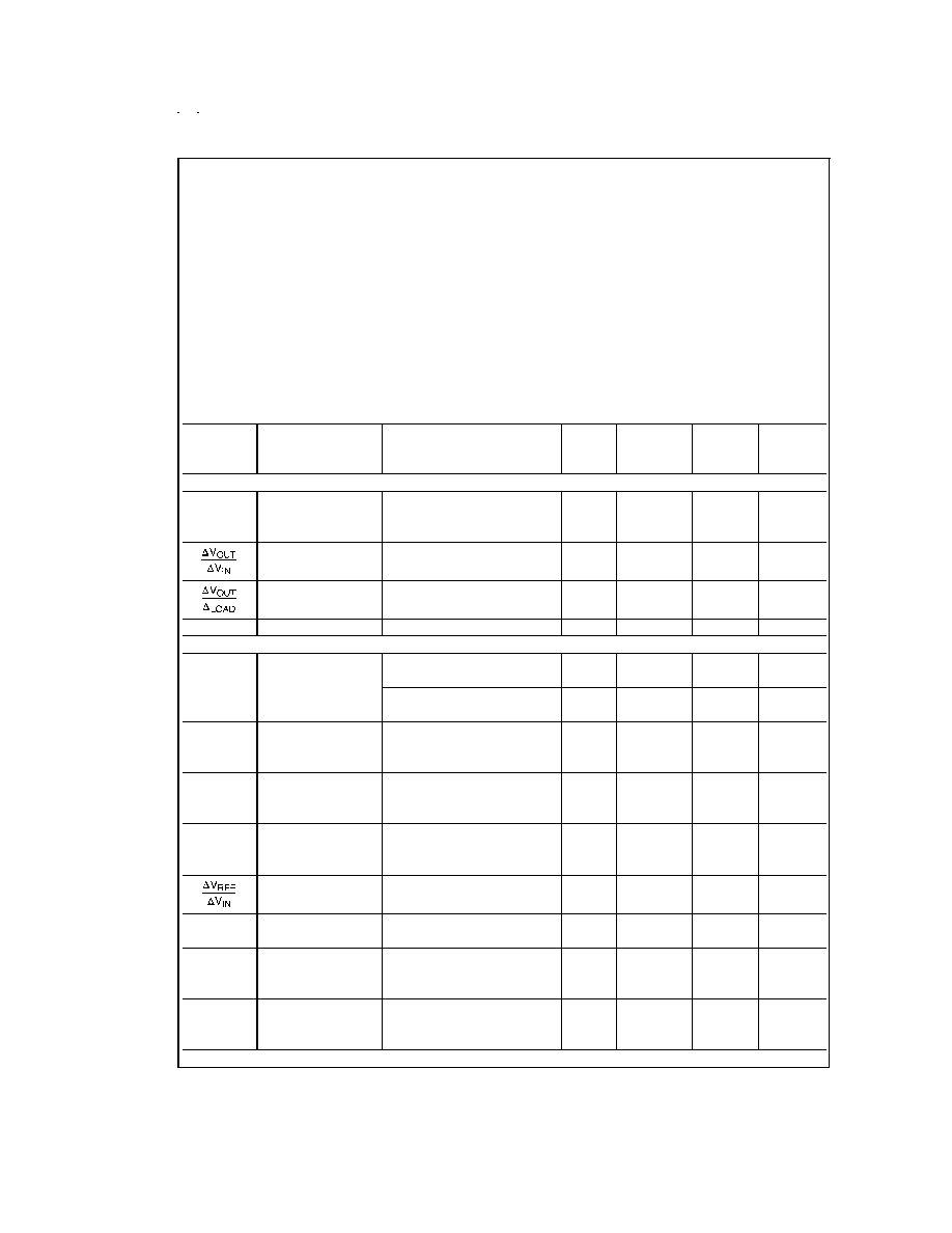
Electrical Characteristics -- LM1577-12, LM2577-12
Specifications with standard type face are for T
J
= 25∞C, and those in bold type face apply over full Operating Temperature
Range. Unless otherwise specified, V
IN
= 5V, and I
SWITCH
= 0.
LM1577-12
LM2577-12
Units
Symbol
Parameter
Conditions
Typical
Limit
Limit
(Limits)
(Notes 3, 4)
(Note 5)
SYSTEM PARAMETERS Circuit of
Figure 1 (Note 6)
V
OUT
Output Voltage
V
IN
= 5V to 10V
12.0
V
I
LOAD
= 100 mA to 800 mA
11.60/11.40
11.60/11.40
V(min)
(Note 3)
12.40/12.60
12.40/12.60
V(max)
Line Regulation
V
IN
= 3.5V to 10V
20
mV
I
LOAD
= 300 mA
50/100
50/100
mV(max)
Load Regulation
V
IN
= 5V
20
mV
I
LOAD
= 100 mA to 800 mA
50/100
50/100
mV(max)
Efficiency
V
IN
= 5V, I
LOAD
= 800 mA
80
%
DEVICE PARAMETERS
I
S
Input Supply Current
V
FEEDBACK
= 14V (Switch Off)
7.5
mA
10.0/14.0
10.0/14.0
mA(max)
I
SWITCH
= 2.0A
25
mA
V
COMP
= 2.0V (Max Duty Cycle)
50/85
50/85
mA(max)
V
UV
Input Supply
I
SWITCH
= 100 mA
2.90
V
Undervoltage Lockout
2.70/2.65
2.70/2.65
V(min)
3.10/3.15
3.10/3.15
V(max)
f
O
Oscillator Frequency
Measured at Switch Pin
52
kHz
I
SWITCH
= 100 mA
48/42
48/42
kHz(min)
56/62
56/62
kHz(max)
V
REF
Output Reference
Measured at Feedback Pin
V
Voltage
V
IN
= 3.5V to 40V
12
11.76/11.64
11.76/11.64
V(min)
V
COMP
= 1.0V
12.24/12.36
12.24/12.36
V(max)
Output Reference
V
IN
= 3.5V to 40V
7
mV
Voltage Line Regulator
R
FB
Feedback Pin Input
9.7
k
Resistance
G
M
Error Amp
I
COMP
= -30 µA to +30 µA
370
µmho
Transconductance
V
COMP
= 1.0V
225/145
225/145
µmho(min)
515/615
515/615
µmho(max)
A
VOL
Error Amp
V
COMP
= 1.1V to 1.9V
80
V/V
Voltage Gain
R
COMP
= 1.0 M
50/25
50/25
V/V(min)
(Note 7)
www.national.com
2

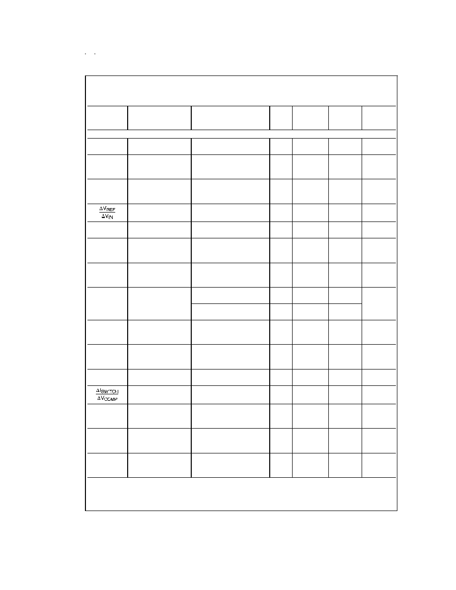
Electrical Characteristics -- LM1577-12, LM2577-12
(Continued)
Specifications with standard type face are for T
J
= 25∞C, and those in bold type face apply over full Operating Temperature
Range. Unless otherwise specified, V
IN
= 5V, and I
SWITCH
= 0.
LM1577-12
LM2577-12
Units
Symbol
Parameter
Conditions
Typical
Limit
Limit
(Limits)
(Notes 3, 4)
(Note 5)
DEVICE PARAMETERS
Error Amplifier
Upper Limit
2.4
V
Output Swing
V
FEEDBACK
= 10.0V
2.2/2.0
2.2/2.0
V(min)
Lower Limit
0.3
V
V
FEEDBACK
= 15.0V
0.40/0.55
0.40/0.55
V(max)
Error Amplifier
V
FEEDBACK
= 10.0V to 15.0V
±
200
µA
Output Current
V
COMP
= 1.0V
±
130/
±
90
±
130/
±
90
µA(min)
±
300/
±
400
±
300/
±
400
µA(max)
I
SS
Soft Start Current
V
FEEDBACK
= 10.0V
5.0
µA
V
COMP
= 0V
2.5/1.5
2.5/1.5
µA(min)
7.5/9.5
7.5/9.5
µA(max)
D
Maximum Duty Cycle
V
COMP
= 1.5V
95
%
I
SWITCH
= 100 mA
93/90
93/90
%(min)
Switch
Transconductance
12.5
A/V
I
L
Switch Leakage
V
SWITCH
= 65V
10
µA
Current
V
FEEDBACK
= 15V (Switch Off)
300/600
300/600
µA(max)
V
SAT
Switch Saturation
I
SWITCH
= 2.0A
0.5
V
Voltage
V
COMP
= 2.0V (Max Duty Cycle)
0.7/0.9
0.7/0.9
V(max)
NPN Switch
4.5
A
Current Limit
3.7/3.0
3.7/3.0
A(min)
5.3/6.0
5.3/6.0
A(max)
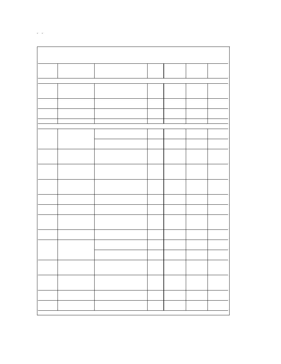
Electrical Characteristics -- LM1577-15, LM2577-15
Specifications with standard type face are for T
J
= 25∞C, and those in bold type face apply over full Operating Temperature
Range. Unless otherwise specified, V
IN
= 5V, and I
SWITCH
= 0.
LM1577-15
LM2577-15
Units
Symbol
Parameter
Conditions
Typical
Limit
Limit
(Limits)
(Notes 3, 4)
(Note 5)
SYSTEM PARAMETERS Circuit of
Figure 2 (Note 6)
V
OUT
Output Voltage
V
IN
= 5V to 12V
15.0
V
I
LOAD
= 100 mA to 600 mA
14.50/14.25
14.50/14.25
V(min)
(Note 3)
15.50/15.75
15.50/15.75
V(max)
Line Regulation
V
IN
= 3.5V to 12V
20
50/100
50/100
mV
I
LOAD
= 300 mA
mV(max)
Load Regulation
V
IN
= 5V
20
50/100
50/100
mV
I
LOAD
= 100 mA to 600 mA
mV(max)
Efficiency
V
IN
= 5V, I
LOAD
= 600 mA
80
%
DEVICE PARAMETERS
I
S
Input Supply Current
V
FEEDBACK
= 18.0V
7.5
mA
(Switch Off)
10.0/14.0
10.0/14.0
mA(max)
I
SWITCH
= 2.0A
25
mA
V
COMP
= 2.0V
50/85
50/85
mA(max)
(Max Duty Cycle)
V
UV
Input Supply
I
SWITCH
= 100 mA
2.90
V
www.national.com
3
Electrical Characteristics -- LM1577-15, LM2577-15
(Continued)
Specifications with standard type face are for T
J
= 25∞C, and those in bold type face apply over full Operating Temperature
Range. Unless otherwise specified, V
IN
= 5V, and I
SWITCH
= 0.
LM1577-15
LM2577-15
Units
Symbol
Parameter
Conditions
Typical
Limit
Limit
(Limits)
(Notes 3, 4)
(Note 5)
DEVICE PARAMETERS
Undervoltage
2.70/2.65
2.70/2.65
V(min)
Lockout
3.10/3.15
3.10/3.15
V(max)
f
O
Oscillator Frequency
Measured at Switch Pin
52
kHz
I
SWITCH
= 100 mA
48/42
48/42
kHz(min)
56/62
56/62
kHz(max)
V
REF
Output Reference
Measured at Feedback Pin
V
Voltage
V
IN
= 3.5V to 40V
15
14.70/14.55
14.70/14.55
V(min)
V
COMP
= 1.0V
15.30/15.45
15.30/15.45
V(max)
Output Reference
V
IN
= 3.5V to 40V
10
mV
Voltage Line Regulation
R
FB
Feedback Pin Input
12.2
k
Voltage Line Regulator
G
M
Error Amp
I
COMP
= -30 µA to +30 µA
300
µmho
Transconductance
V
COMP
= 1.0V
170/110
170/110
µmho(min)
420/500
420/500
µmho(max)
A
VOL
Error Amp
V
COMP
= 1.1V to 1.9V
65
V/V
Voltage Gain
R
COMP
= 1.0 M
40/20
40/20
V/V(min)
(Note 7)
Error Amplifier
Upper Limit
2.4
V
Output Swing
V
FEEDBACK
= 12.0V
2.2/2.0
2.2/2.0
V(min)
Lower Limit
0.3
V
V
FEEDBACK
= 18.0V
0.4/0.55
0.40/0.55
V(max)
Error Amp
V
FEEDBACK
= 12.0V to 18.0V
±
200
µA
Output Current
V
COMP
= 1.0V
±
130/
±
90
±
130/
±
90
µA(min)
±
300/
±
400
±
300/
±
400
µA(max)
I
SS
Soft Start Current
V
FEEDBACK
= 12.0V
5.0
µA
V
COMP
= 0V
2.5/1.5
2.5/1.5
µA(min)
7.5/9.5
7.5/9.5
µA(max)
D
Maximum Duty
V
COMP
= 1.5V
95
%
Cycle
I
SWITCH
= 100 mA
93/90
93/90
%(min)
Switch
Transconductance
12.5
A/V
I
L
Switch Leakage
V
SWITCH
= 65V
10
µA
Current
V
FEEDBACK
= 18.0V
300/600
300/600
µA(max)
(Switch Off)
V
SAT
Switch Saturation
I
SWITCH
= 2.0A
0.5
V
Voltage
V
COMP
= 2.0V
0.7/0.9
0.7/0.9
V(max)
(Max Duty Cycle)
NPN Switch
V
COMP
= 2.0V
4.3
A
Current Limit
3.7/3.0
3.7/3.0
A(min)
5.3/6.0
5.3/6.0
A(max)
www.national.com
4
Electrical Characteristics -- LM1577-ADJ, LM2577-ADJ
Specifications with standard type face are for T
J
= 25∞C, and those in bold type face apply over full Operating Temperature
Range. Unless otherwise specified, V
IN
= 5V, V
FEEDBACK
= V
REF
, and I
SWITCH
= 0.
LM1577-ADJ LM2577-ADJ
Units
Symbol
Parameter
Conditions
Typical
Limit
Limit
(Limits)
(Notes 3, 4)
(Note 5)
SYSTEM PARAMETERS Circuit of
Figure 3 (Note 6)
V
OUT
Output Voltage
V
IN
= 5V to 10V
12.0
V
I
LOAD
= 100 mA to 800 mA
11.60/11.40
11.60/11.40
V(min)
(Note 3)
12.40/12.60
12.40/12.60
V(max)
V
OUT
/
Line Regulation
V
IN
= 3.5V to 10V
20
mV
V
IN
I
LOAD
= 300 mA
50/100
50/100
mV(max)
V
OUT
/
Load Regulation
V
IN
= 5V
20
mV
I
LOAD
I
LOAD
= 100 mA to 800 mA
50/100
50/100
mV(max)
Efficiency
V
IN
= 5V, I
LOAD
= 800 mA
80
%
DEVICE PARAMETERS
I
S
Input Supply Current
V
FEEDBACK
= 1.5V (Switch Off)
7.5
mA
10.0/14.0
10.0/14.0
mA(max)
I
SWITCH
= 2.0A
25
mA
V
COMP
= 2.0V (Max Duty Cycle)
50/85
50/85
mA(max)
V
UV
Input Supply
I
SWITCH
= 100 mA
2.90
V
Undervoltage Lockout
2.70/2.65
2.70/2.65
V(min)
3.10/3.15
3.10/3.15
V(max)
f
O
Oscillator Frequency
Measured at Switch Pin
52
kHz
I
SWITCH
= 100 mA
48/42
48/42
kHz(min)
56/62
56/62
kHz(max)
V
REF
Reference
Measured at Feedback Pin
V
Voltage
V
IN
= 3.5V to 40V
1.230
1.214/1.206
1.214/1.206
V(min)
V
COMP
= 1.0V
1.246/1.254
1.246/1.254
V(max)
V
REF
/
Reference Voltage
V
IN
= 3.5V to 40V
0.5
mV
V
IN
Line Regulation
I
B
Error Amp
V
COMP
= 1.0V
100
nA
Input Bias Current
300/800
300/800
nA(max)
G
M
Error Amp
I
COMP
= -30 µA to +30 µA
3700
µmho
Transconductance
V
COMP
= 1.0V
2400/1600
2400/1600
µmho(min)
4800/5800
4800/5800
µmho(max)
A
VOL
Error Amp
V
COMP
= 1.1V to 1.9V
800
V/V
Voltage Gain
R
COMP
= 1.0 M
(Note 7)
500/250
500/250
V/V(min)
Error Amplifier
Upper Limit
2.4
V
Output Swing
V
FEEDBACK
= 1.0V
2.2/2.0
2.2/2.0
V(min)
Lower Limit
0.3
V
V
FEEDBACK
= 1.5V
0.40/0.55
0.40/0.55
V(max)
Error Amp
V
FEEDBACK
= 1.0V to 1.5V
±
200
µA
Output Current
V
COMP
= 1.0V
±
130/
±
90
±
130/
±
90
µA(min)
±
300/
±
400
±
300/
±
400
µA(max)
I
SS
Soft Start Current
V
FEEDBACK
= 1.0V
5.0
µA
V
COMP
= 0V
2.5/1.5
2.5/1.5
µA(min)
7.5/9.5
7.5/9.5
µA(max)
D
Maximum Duty Cycle
V
COMP
= 1.5V
95
%
I
SWITCH
= 100 mA
93/90
93/90
%(min)
I
SWITCH
/
Switch
12.5
A/V
V
COMP
Transconductance
www.national.com
5