LM2672
SIMPLE SWITCHER
®
Power Converter High Efficiency
1A Step-Down Voltage Regulator with Features
General Description
The LM2672 series of regulators are monolithic integrated
circuits built with a LMDMOS process. These regulators
provide all the active functions for a step-down (buck)
switching regulator, capable of driving a 1A load current with
excellent line and load regulation. These devices are avail-
able in fixed output voltages of 3.3V, 5.0V, 12V, and an
adjustable output version.
Requiring a minimum number of external components, these
regulators are simple to use and include patented internal
frequency compensation (Patent Nos. 5,382,918 and
5,514,947), fixed frequency oscillator, external shutdown,
soft-start, and frequency synchronization.
The LM2672 series operates at a switching frequency of
260 kHz, thus allowing smaller sized filter components than
what would be needed with lower frequency switching regu-
lators. Because of its very high efficiency (
>
90%), the cop-
per traces on the printed circuit board are the only heat
sinking needed.
A family of standard inductors for use with the LM2672 are
available from several different manufacturers. This feature
greatly simplifies the design of switch-mode power supplies
using these advanced ICs. Also included in the datasheet
are selector guides for diodes and capacitors designed to
work in switch-mode power supplies.
Other features include a guaranteed
±
1.5% tolerance on
output voltage within specified input voltages and output
load conditions, and
±
10% on the oscillator frequency. Ex-
ternal shutdown is included, featuring typically 50 µA
stand-by current. The output switch includes current limiting,
as well as thermal shutdown for full protection under fault
conditions.
To simplify the LM2672 buck regulator design procedure,
there exists computer design software, LM267X Made
Simple version 1.0.
Features
n
Efficiency up to 96%
n
Available in SO-8 and 8-pin DIP packages
n
Computer Design Software LM267X Made Simple
version 1.0
n
Simple and easy to design with
n
Requires only 5 external components
n
Uses readily available standard inductors
n
3.3V, 5.0V, 12V, and adjustable output versions
n
Adjustable version output voltage range: 1.21V to 37V
n
±
1.5% max output voltage tolerance over line and load
conditions
n
Guaranteed 1A output load current
n
0.25
DMOS Output Switch
n
Wide input voltage range: 8V to 40V
n
260 kHz fixed frequency internal oscillator
n
TTL shutdown capability, low power standby mode
n
Soft-start and frequency synchronization
n
Thermal shutdown and current limit protection
Typical Applications
n
Simple High Efficiency (
>
90%) Step-Down (Buck)
Regulator
n
Efficient Pre-Regulator for Linear Regulators
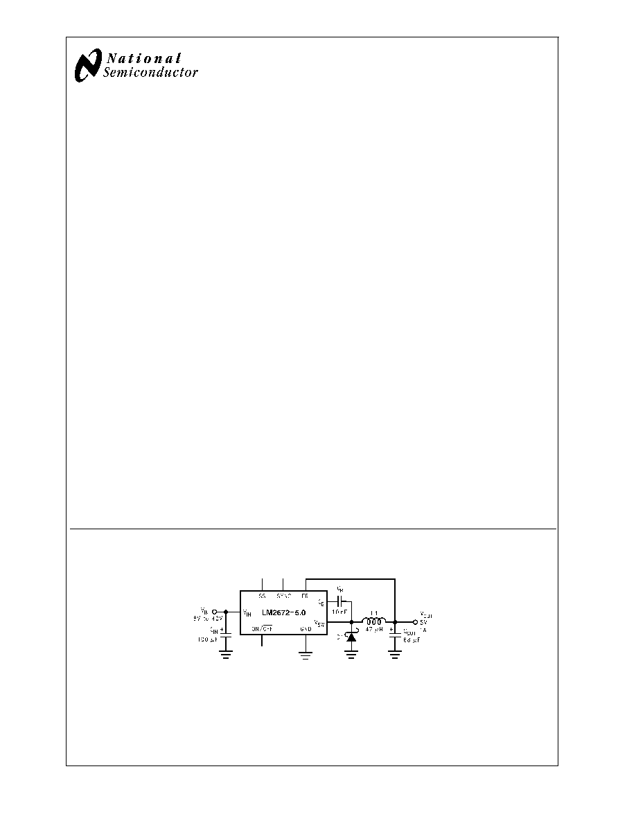
Typical Application
(Fixed Output Voltage
Versions)
01293401
SIMPLE SWITCHER
®
is a registered trademark of National Semiconductor Corporation.
Windows
®
is a registered trademark of Microsoft Corporation.
February 2005
LM2672
SIMPLE
SWITCHER
Power
Converter
High
Efficiency
1A
Step-Down
V
oltage
Regulator
with
Features
© 2005 National Semiconductor Corporation
DS012934
www.national.com
Absolute Maximum Ratings
(Note 1)
If Military/Aerospace specified devices are required,
please contact the National Semiconductor Sales Office/
Distributors for availability and specifications.
Supply Voltage
45V
ON/OFF Pin Voltage
-0.1V
V
SH
6V
Switch Voltage to Ground
-1V
Boost Pin Voltage
V
SW
+ 8V
Feedback Pin Voltage
-0.3V
V
FB
14V
ESD Susceptibility
Human Body Model (Note 2)
2 kV
Power Dissipation
Internally Limited
Storage Temperature Range
-65°C to +150°C
Lead Temperature
M Package
Vapor Phase (60s)
+215°C
Infrared (15s)
+220°C
N Package (Soldering, 10s)
+260°C
Maximum Junction Temperature
+150°C
Operating Ratings
Supply Voltage
6.5V to 40V
Temperature Range
-40°C
T
J
+125°C
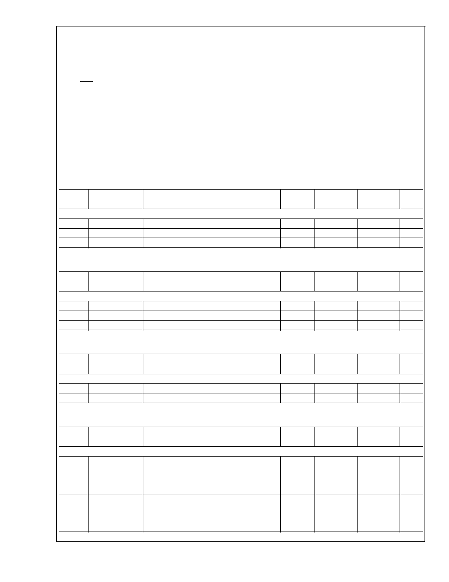
Electrical Characteristics
Specifications with standard type face are for T
J
= 25°C, and those in bold type
face apply over full Operating Temperature Range.
LM2672-3.3
Symbol
Parameter
Conditions
Typical
Min
Max
Units
(Note 4)
(Note 5)
(Note 5)
SYSTEM PARAMETERS Test Circuit Figure 2 (Note 3)
V
OUT
Output Voltage
V
IN
= 8V to 40V, I
LOAD
= 20 mA to 1A
3.3
3.251/3.201
3.350/3.399
V
V
OUT
Output Voltage
V
IN
= 6.5V to 40V, I
LOAD
= 20 mA to 500 mA
3.3
3.251/3.201
3.350/3.399
V
Efficiency
V
IN
= 12V, I
LOAD
= 1A
86
%
LM2672-5.0
Symbol
Parameter
Conditions
Typical
Min
Max
Units
(Note 4)
(Note 5)
(Note 5)
SYSTEM PARAMETERS Test Circuit Figure 2 (Note 3)
V
OUT
Output Voltage
V
IN
= 8V to 40V, I
LOAD
= 20 mA to 1A
5.0
4.925/4.850
5.075/5.150
V
V
OUT
Output Voltage
V
IN
= 6.5V to 40V, I
LOAD
= 20 mA to 500 mA
5.0
4.925/4.850
5.075/5.150
V
Efficiency
V
IN
= 12V, I
LOAD
= 1A
90
%
LM2672-12
Symbol
Parameter
Conditions
Typical
Min
Max
Units
(Note 4)
(Note 5)
(Note 5)
SYSTEM PARAMETERS Test Circuit Figure 2 (Note 3)
V
OUT
Output Voltage
V
IN
= 15V to 40V, I
LOAD
= 20 mA to 1A
12
11.82/11.64
12.18/12.36
V
Efficiency
V
IN
= 24V, I
LOAD
= 1A
94
%
LM2672-ADJ
Symbol
Parameter
Conditions
Typ
Min
Max
Units
(Note 4)
(Note 5)
(Note 5)
SYSTEM PARAMETERS Test Circuit Figure 3 (Note 3)
V
FB
Feedback
Voltage
V
IN
= 8V to 40V, I
LOAD
= 20 mA to 1A
1.210
1.192/1.174
1.228/1.246
V
V
OUT
Programmed for 5V
(see Circuit of Figure 3)
V
FB
Feedback
Voltage
V
IN
= 6.5V to 40V, I
LOAD
= 20 mA to 500 mA
1.210
1.192/1.174
1.228/1.246
V
V
OUT
Programmed for 5V
(see Circuit of Figure 3)
LM2672
www.national.com
2
LM2672-ADJ
(Continued)
Symbol
Parameter
Conditions
Typ
Min
Max
Units
(Note 4)
(Note 5)
(Note 5)
Efficiency
V
IN
= 12V, I
LOAD
= 1A
90
%
All Output Voltage Versions
Electrical Characteristics
Specifications with standard type face are for T
J
= 25°C, and those in bold type face apply over full Operating Temperature
Range. Unless otherwise specified, V
IN
= 12V for the 3.3V, 5V, and Adjustable versions and V
IN
= 24V for the 12V version,
and I
LOAD
= 100 mA.
Symbol
Parameters
Conditions
Typ
Min
Max
Units
DEVICE PARAMETERS
I
Q
Quiescent Current
V
FEEDBACK
= 8V
2.5
3.6
mA
For 3.3V, 5.0V, and ADJ Versions
V
FEEDBACK
= 15V
2.5
mA
For 12V Versions
I
STBY
Standby Quiescent Current
ON/OFF Pin = 0V
50
100/150
µA
I
CL
Current Limit
1.55
1.25/1.2
2.1/2.2
A
I
L
Output Leakage Current
V
IN
= 40V, ON/OFF Pin = 0V
1
25
µA
V
SWITCH
= 0V
V
SWITCH
= -1V, ON/OFF Pin = 0V
6
15
mA
R
DS(ON)
Switch On-Resistance
I
SWITCH
= 1A
0.25
0.30/0.50
f
O
Oscillator Frequency
Measured at Switch Pin
260
225
275
kHz
D
Maximum Duty Cycle
95
%
Minimum Duty Cycle
0
%
I
BIAS
Feedback Bias
V
FEEDBACK
= 1.3V
85
nA
Current
ADJ Version Only
V
S/D
ON/OFF Pin
1.4
0.8
2.0
V
Voltage Thesholds
I
S/D
ON/OFF Pin Current
ON/OFF Pin = 0V
20
7
37
µA
F
SYNC
Synchronization Frequency
V
SYNC
= 3.5V, 50% duty cycle
400
kHz
V
SYNC
Synchronization Threshold
Voltage
1.4
V
V
SS
Soft-Start Voltage
0.63
0.53
0.73
V
I
SS
Soft-Start Current
4.5
1.5
6.9
µA
JA
Thermal Resistance
N Package, Junction to Ambient (Note 6)
95
°C/W
M Package, Junction to Ambient (Note 6)
105
Note 1: Absolute Maximum Ratings indicate limits beyond which damage to the device may occur. Operating Ratings indicate conditions for which the device is
intended to be functional, but device parameter specifications may not be guaranteed under these conditions. For guaranteed specifications and test conditions, see
the Electrical Characteristics.
Note 2: The human body model is a 100 pF capacitor discharged through a 1.5 k
resistor into each pin.
Note 3: External components such as the catch diode, inductor, input and output capacitors, and voltage programming resistors can affect switching regulator
performance. When the LM2672 is used as shown in Figure 2 and Figure 3 test circuits, system performance will be as specified by the system parameters section
of the Electrical Characteristics.
Note 4: Typical numbers are at 25°C and represent the most likely norm.
Note 5: All limits guaranteed at room temperature (standard type face) and at temperature extremes (bold type face). All room temperature limits are 100%
production tested. All limits at temperature extremes are guaranteed via correlation using standard Statistical Quality Control (SQC) methods. All limits are used
to calculate Average Outgoing Quality Level (AOQL).
Note 6: Junction to ambient thermal resistance with approximately 1 square inch of printed circuit board copper surrounding the leads. Additional copper area will
lower thermal resistance further. See Application Information section in the application note accompanying this datasheet and the thermal model in LM267X Made
Simple version 1.0 software.
LM2672
www.national.com
3
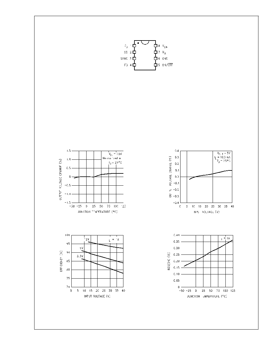
Connection Diagram
8-Lead Package
Top View
01293402
For Surface Mount Package
Order Number
LM2672M-3.3, LM2672M-5.0,
LM2672M-12 or LM2672M-ADJ
See NSC Package Number M08A
For DIP Package
Order Number
LM2672N-3.3, LM2672N-5.0,
LM2672N-12 or LM2672N-ADJ
See NSC Package Number N08E
Typical Performance Characteristics
Normalized
Output Voltage
Line Regulation
01293403
01293404
Efficiency
Drain-to-Source
Resistance
01293405
01293406
LM2672
www.national.com
4