 | ÐлекÑÑоннÑй компоненÑ: LM2793 | СкаÑаÑÑ:  PDF PDF  ZIP ZIP |
Äîêóìåíòàöèÿ è îïèñàíèÿ www.docs.chipfind.ru
LM2793
Low Noise White LED Constant Current Supply with
Dual Function Brightness Control
General Description
The LM2793 is a highly efficient, semi-regulated 1.5x CMOS
charge pump that provides dual constant current outputs.
The LM2793 has an input voltage range of 2.7V to 5.5V.
To control LED brightness, the amount of current driven to
the current-mode outputs can be adjusted with an analog
voltage and/or a pulse-width-modulated (PWM) square
wave.
Pre-regulation of the charge pump minimizes conducted
noise on the input. Combined with a fixed switching fre-
quency of 500kHz, the LM2793 is a low-noise solution.
The LM2793 is available in a 10-pin Leadless Lead-frame
package: LLP-10.
Features
n
Two Regulated Current Outputs, up to 16mA Each,
Matched to Within
±
0.3% (typ.)
n
High Efficiency, 1.5x Regulated Charge Pump
n
Input Voltage Range: 2.7V to 5.5V
n
Soft Start Limits Inrush Current
n
Analog Voltage Brightness Control
n
PWM Brightness Control
n
Very Small Solution Size - NO INDUCTOR
n
500kHz Switching Frequency
n
3µA (typ.) Shutdown Current
n
LLP-10 Package: 3.0mm X 3.0mm X 0.8mm
Applications
n
White LED Display Backlights
n
White LED Keypad Backlights
n
1-Cell LiIon Battery-Operated Equipment Including
PDAs, Hand-held PCs, Cellular Phones
n
Flat Panel Displays
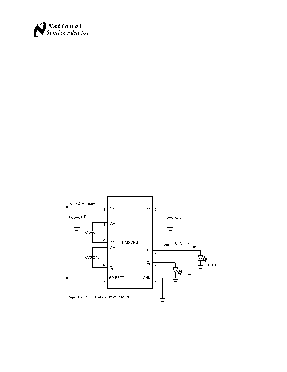
Typical Application Circuit
20063602
February 2003
LM2793
Low
Noise
White
LED
Constant
Current
Supply
with
Dual
Function
Brightness
Control
© 2003 National Semiconductor Corporation
DS200636
www.national.com
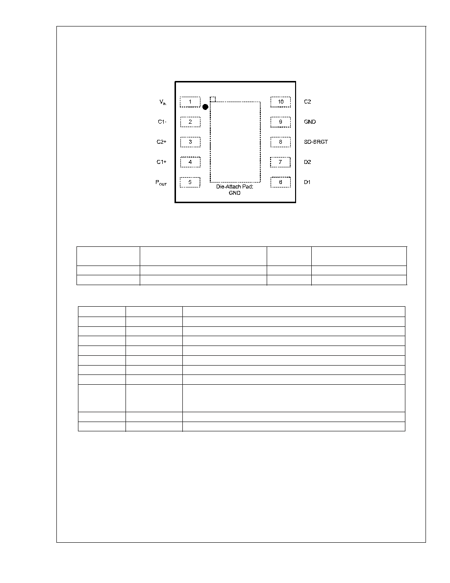
Connection Diagram
LM2793
10-pin Leadless Leadframe Package (LLP-10)
3mmx3mmx0.8mm
NS Package Number LDA10A
20063603
Top View
Ordering Information
Order Number
Package Description
Package
Marking
Supplied as Tape and Reel
(Units)
LM2793LD
LLP-10
LM2793
1000
LM2793LDX
LLP-10
LM2793
4500
Pin Description
Pin
Name
Description
1
V
IN
Power supply voltage connection
2
C1-
Flying capacitor C1 connection
3
C2+
Flying capacitor C2 connection
4
C1+
Flying capacitor C1 connection
5
P
OUT
Charge pump output
6
D1
Current source output / LED connection
7
D2
Current source output / LED connection
8
SD-BRGT
Dual function Shutdown - Brightness. Grounding pin shuts down part. Voltage
between 0.75V and 2.75V (typ.) linearly adjusts current outputs. Output current
equals 16mA at voltages above 2.75V.
9
GND
Power supply ground connection
10
C2-
Flying capacitor C2 connection
LM2793
www.national.com
2
Absolute Maximum Ratings
(Notes 1,
2)
If Military/Aerospace specified devices are required,
please contact the National Semiconductor Sales Office/
Distributors for availability and specifications.
V
IN
-0.3V to 6.0V
V
SD-BRGT
-0.3V to (V
IN
+
0.3V) w/ 6.0V max
Continuous Power Dissipation (Note
4)
Internally Limited
Junction Temperature (T
J-MAX-ABS
)
150°C
Storage Temperature Range
-65°C to 150°C
Lead Temp. (Soldering, 5 sec.)
260°C
ESD Rating (Note 5)
Human Body Model
2kV
Machine Model
200V
Operating Ratings
(Notes 2, 8)
Input Voltage V
IN
2.7V to 5.5V
V
SD-BRGT
0V to V
IN
Brightness Adjustment Control
Range of V
SD-BRGT
0.75V to 2.75V
Junction Temperature Range (T
J
)
-30°C to +100°C
Ambient Temperature Range (T
A
)
-30°C to +85 °C
(Note 6)
Thermal Information
Junction-to-Ambient Thermal
Resistance,
LLP-10 Package (
JA
) (Note 7)
55°C/W
Electrical Characteristics
(Notes 2, 8)
Limits in standard typeface are for T
J
= 25°C, and limits in boldface type apply over the full operating junction temprature
range. Unless otherwise specified: C
1
=C
2
=C
IN
=C
HOLD
=1µF; V
IN
=3.6V; V
SD-BRGT
=3.0V; V
DX
=3.6V
Symbol
Parameter
Conditions
Min
Typ
Max
Units
I
DX
Output Current Regulation
3.3V
V
IN
5.5V
V
DX
= 3.9V
14.7
13.7
15.9
17.2
17.3
mA
3.0V
V
IN
5.5V
V
DX
= 3.8V
14.7
13.7
15.9
17.2
17.3
2.7V
V
IN
5.5V
V
DX
= 3.4V
14.7
13.7
15.9
17.2
17.3
2.5V
V
DX
3.9V
(Note 9)
14.7
13.7
15.9
17.2
17.3
V
SD-BRGT
= 2.0V
10
V
SD-BRGT
= 0.75V
0.1
I
D-MATCH
I
D1
-to-I
D2
Current Matching
0.3
3.0
%
R
OUT
Charge Pump Output
Resistance
V
IN
= 2.7V
3.5
V
HR-min
Minimum Current Source
Voltage Headroom (V
POUT
-
V
IDx
) (Note 10)
I
DX
= 16mA
400
mV
I
Q
Quiescent Supply Current
I
DX
, I
POUT
= 0
1.2
2.2
mA
I
SD
Shutdown Supply Current
2.7V
V
IN
5.5V
V
SD-BRGT
= 0V
3
5
µA
ON/OFF
SD-BRGT Pin Thresholds
for Active and Shutdown
Modes
Active
V
IN
= 3.0V
0.70
V
Shutdown
V
IN
= 3.0V
0.25
I
LEAK-SD
SD-BRGT Pin Leakage
Current
17
µA
f
SW
Switching Frequency
2.7V
V
IN
5.5V
325
500
675
kHz
t
START
Startup Time
I
DX
= 90% steady state
30
µs
Note 1: Absolute Maximum Ratings indicate limits beyond which damage to the component may occur. Operating Ratings are conditions under which operation of
the device is guaranteed. Operating Ratings do not imply guaranteed performance limits. For guaranteed performance limits and associated test conditions, see the
Electrical Characteristics tables.
Note 2: All voltages are with respect to the potential at the GND pin.
Note 3: Voltage on the SD-BRGT pin should not exceed 6V.
Note 4: Thermal shutdown circuitry protects the device from permanent damage. D
1
and D
2
may be shorted to GND without damage.
LM2793
www.national.com
3
Electrical Characteristics
(Notes 2, 8)
(Continued)
Note 5: The human-body model is a 100 pF capacitor discharged through a 1.5 k resistor into each pin. The machine model is a 200pF capacitor discharged directly
into each pin.
Note 6: Maximum ambient temperature (T
A-MAX
) is dependent on the maximum operating junction temperature (T
J-MAX-OP
= 100
o
C), the maximum power
dissipation of the device in the application (P
D-MAX
), and the junction-to-ambient thermal resistance of the part/package in the application (
JA
), as given by the
following equation: T
A-MAX
= T
J-MAX-OP
- (
JA
x P
D-MAX
). The ambient temperature operating rating is provided merely for convenience. This part may be operated
outside the listed T
A
rating, so long as the junction temperature of the device does not exceed the maximum operating rating of 100
o
C.
Note 7: Junction-to-ambient thermal resistance is highly application and board-layout dependent. In applications where high maximum power dissipation exists,
special care must be paid to thermal dissipation issues. For more information on these topics, please refer to the Power Dissipation section of this datasheet.
Note 8: All room temperature limits are 100% tested or guaranteed through statistical analysis. All limits at temperature extremes are guaranteed by correlation
using standard Statistical Quality Control methods (SQC). All limits are used to calculate Average Outgoing Quality Level (AOQL). Typical numbers are not
guaranteed, but do represent the most likely norm.
Note 9: Maximum LED voltage (V
Dx
) is highly dependent on the application's minimum input voltage and the amount of current flowing through the LEDs. Maximum
LED voltage for a given application can be approximated with the following equations:
V
IN-MIN
<
3.0V: V
Dx-MAX
= (1.5 x V
IN-MIN
) - (I
DX
x 25 mV/mA) - (3.5
x 2 x I
DX
)
V
IN-MIN
3.0V: V
Dx-MAX
= 4.3V - (I
DX
x 25 mV/mA)
The equations above assume LEDs are connected to outputs D
1
and D
2
, and no current drawn from the charge pump output (P
OUT
). For a more precise and
thorough analysis of maximum LED voltage, please refer to text sections of the datasheet (to appear in future datasheet revisions - in the interim, please contact
National Semiconductor for more information).
Note 10: Current sources are connected internally between P
OUT
and I
Dx
. The voltage across each current source, [V(P
OUT
) - V(I
Dx
)], is referred to as headroom
voltage. For current sources to regulate properly, a minimum headroom voltage must be present across them. Minimum required headroom voltage is proportional
to the current flowing through the current source, as dictated by this equation: V
HR-min
= 400mV x (I
Dx
/ 16mA).
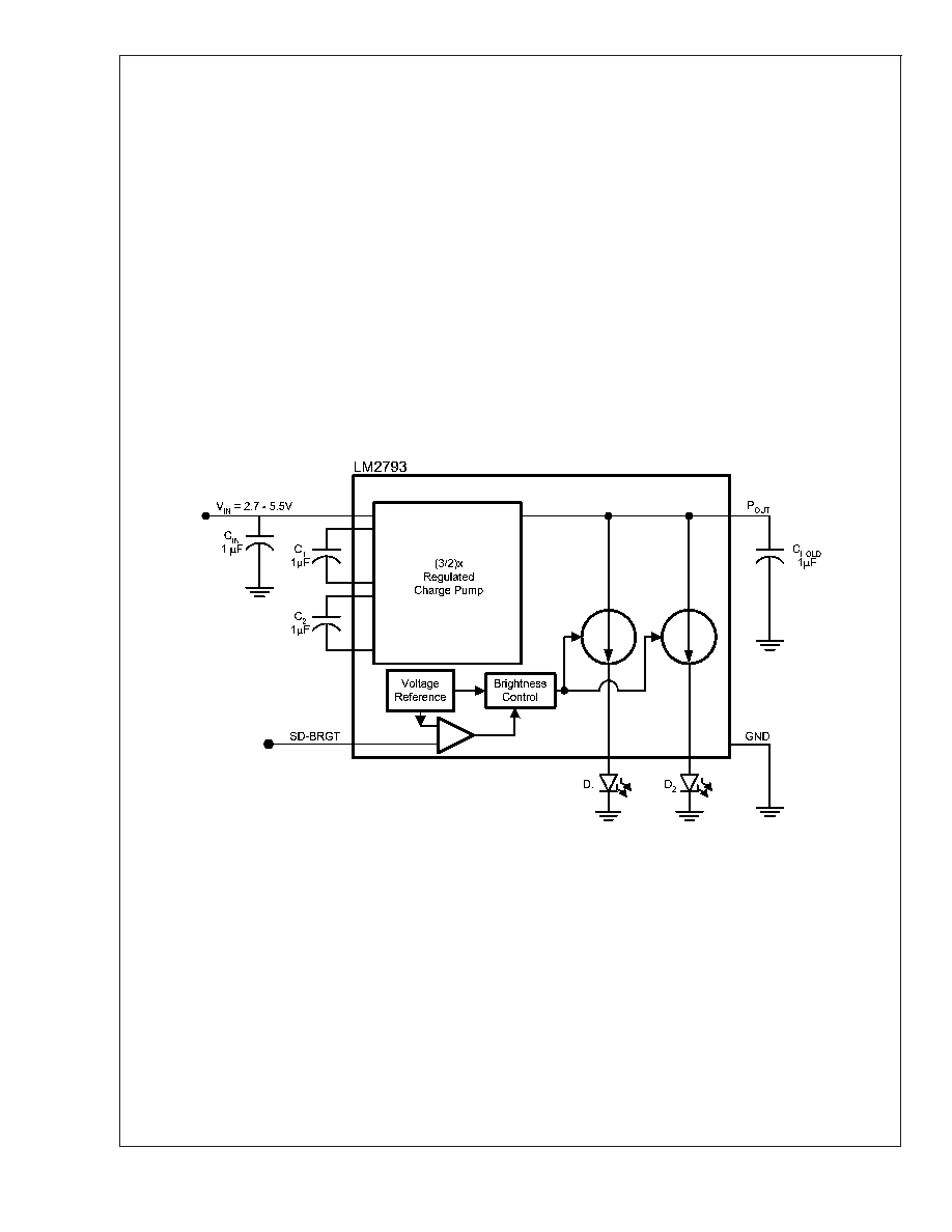
Block Diagram
20063601
LM2793
www.national.com
4
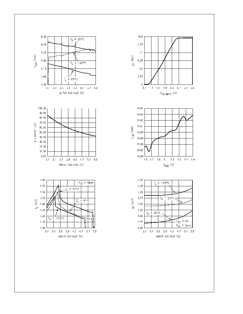
Typical Performance Characteristics
Unless otherwise specified: T
A
= 25°C, 2 LEDs, V
DX
= 3.6V,
V
IN
= 3.6, V
SD-BRGT
= 3.0, C
1
= C
2
= C
IN
= C
HOLD
= 1µF. Capacitors are low-ESR multi-layer ceramic capacitors (MLCC's).
LED Current vs. Input Voltage
LED Current vs. SD-BRGT Voltage
20063606
20063607
Efficiency vs. Input Voltage
LED Current vs. LED Voltage
20063612
20063608
Quiescent Current vs. Input Voltage
Shutdown Supply Current vs. Input Voltage
20063609
20063610
LM2793
www.national.com
5
Document Outline