
LM2937-2.5, LM2937-3.3
400mA and 500mA Voltage Regulators
General Description
The LM2937-2.5 and LM2937-3.3 are positive voltage regu-
lators capable of supplying up to 500 mA of load current.
Both regulators are ideal for converting a common 5V logic
supply, or higher input supply voltage, to the lower 2.5V and
3.3V supplies to power VLSI ASIC's and microcontrollers.
Special circuitry has been incorporated to minimize the qui-
escent current to typically only 10 mA with a full 500 mA load
current when the input to output voltage differential is greater
than 5V.
The LM2937 requires an output bypass capacitor for stabil-
ity. As with most regulators utilizing a PNP pass transistor,
the ESR of this capacitor remains a critical design param-
eter, but the LM2937-2.5 and LM2937-3.3 include special
compensation circuitry that relaxes ESR requirements. The
LM2937 is stable for all ESR ratings less than 5
. This al-
lows the use of low ESR chip capacitors.
The regulators are also suited for automotive applications,
with built in protection from reverse battery connections,
two-battery jumps and up to +60V/-50V load dump tran-
sients. Familiar regulator features such as short circuit and
thermal shutdown protection are also built in.
Features
n
Fully specified for operation over -40∞C to +125∞C
n
Output current in excess of 500 mA (400mA for
SOT-223 package)
n
Output trimmed for 5% tolerance under all operating
conditions
n
Wide output capacitor ESR range, 0.01
up to 5
n
Internal short circuit and thermal overload protection
n
Reverse battery protection
n
60V input transient protection
n
Mirror image insertion protection
Connection Diagram and Ordering Information
TO-220 Plastic Package
DS100113-24
Front View
Order Number LM2937ET-2.5, LM2937ET-3.3,
See NS Package Number T03B
SOT-223 Plastic Package
DS100113-25
Front View
Order Number LM2937IMP-2.5, LM2937IMP-3.3,
See NS Package Number MA04A
TO-263 Surface-Mount Package
DS100113-26
Top View
DS100113-27
Side View
Order Number LM2937ES-2.5, LM2937ES-3.3,
See NS Package Number TS3B
February 1998
LM2937-2.5,
LM2937-3.3
400mA
and
500mA
V
oltage
Regulators
© 1998 National Semiconductor Corporation
DS100113
www.national.com

Connection Diagram and Ordering Information
(Continued)
Temperature
Range
Output Voltage
NSC
Package
2.5
3.3
Package
Drawing
-40∞C
T
A
125∞C
LM2937ES-2.5
LM2937ES-3.3
TS3B
TO-263
LM2937ET-2.5
LM2937ET-3.3
T03B
TO-220
-40∞C
T
A
85∞C
LM2937IMP-2.5
LM2937IMP-3.3
MA04A
SOT-223
SOT-223 Package
Markings
L68B
L69B
The small physical size of the SOT-223 package does not allow sufficient space to provide the complete device part number. The actual devices will be labeled with
the package markings shown.
www.national.com
2

Absolute Maximum Ratings
(Note 1)
If Military/Aerospace specified devices are required,
please contact the National Semiconductor Sales Office/
Distributors for availability and specifications.
Input Voltage
Continuous
26V
Transient (t
100 ms)
60V
Internal Power Dissipation (Note 2)
Internally Limited
Maximum Junction Temperature
150∞C
Storage Temperature Range
-65∞C to +150∞C
Lead Temperature Soldering
TO-220 (10 seconds)
260∞C
TO-263 (10 seconds)
230∞C
SOT-223 (Vapor Phase, 60 seconds)
215∞C
SOT-223 (Infrared, 15 seconds)
220∞C
ESD Susceptibility (Note 3)
2 kV
Operating Conditions
(Note 1)
Temperature Range (Note 2)
LM2937ES, LM2937ET
-40∞C
T
A
125∞C
LM2937IMP
-40∞C
T
A
85∞C
Input Voltage Range
4.75V to 26V
Electrical Characteristics
(Note 4)
V
IN
= V
NOM
+ 5V, I
OUTmax
= 500 mA for the TO-220 and TO-263 packages, I
OUTmax
=400mA for the SOT-223 package, C
OUT
= 10 µF unless otherwise indicated. Boldface limits apply over the entire operating temperature range, of the indicated
device, all other specifications are for T
A
= T
J
= 25∞C.
Output Voltage (V
OUT
)
2.5V
3.3V
Units
Parameter
Conditions
Typ
Limit
Typ
Limit
Output Voltage
5 mA
I
OUT
I
OUTmax
2.42
3.20
V (Min)
2.5
2.38
3.3
3.14
V(Min)
2.56
3.40
V(Max)
2.62
3.46
V(Max)
Line Regulation(Note 5)
4.75V
V
IN
26V,
7.5
25
9.9
33
mV(Max)
I
OUT
= 5 mA
Load Regulation
5 mA
I
OUT
I
OUTmax
2.5
25
3.3
33
mV(Max)
Quiescent Current
7V
V
IN
26V,
2
10
2
10
mA(Max)
I
OUT
= 5 mA
V
IN
= (V
OUT
+ 5V),
10
20
10
20
mA(Max)
I
OUT
= I
OUTmax
V
IN
= 5V, I
OUT
= I
OUTmax
66
100125
66
100125
mA(Max)
Output Noise
10 Hz≠100 kHz,
75
99
µVrms
Voltage
I
OUT
= 5 mA
Long Term Stability
1000 Hrs.
10
13.2
mV
Short-Circuit Current
1.0
0.6
1.0
0.6
A(Min)
Peak Line Transient
t
f
<
100 ms, R
L
= 100
75
60
75
60
V(Min)
Voltage
Maximum Operational
26
26
V(Min)
Input Voltage
Reverse DC
V
OUT
-0.6V, R
L
= 100
-30
-15
-30
-15
V(Min)
Input Voltage
Reverse Transient
t
r
<
1 ms, R
L
= 100
-75
-50
-75
-50
V(Min)
Input Voltage
Note 1: Absolute Maximum Ratings indicate limits beyond which damage to the device may occur. Electrical specifications do not apply when operating the device
outside of its rated Operating Conditions.
Note 2: The maximum allowable power dissipation at any ambient temperature is P
MAX
= (125 - T
A
)/
JA
, where 125 is the maximum junction temperature for op-
eration, T
A
is the ambient temperature, and
JA
is the junction-to-ambient thermal resistance. If this dissipation is exceeded, the die temperature will rise above 125∞C
and the electrical specifications do not apply. If the die temperature rises above 150∞C, the regulator will go into thermal shutdown. The junction-to-ambient thermal
resistance
JA
is 65∞C/W, for the TO-220 package, 73∞C/W for the TO-263 package, and 174∞C/W for the SOT-223 package. When used with a heatsink,
JA
is the
sum of the device junction-to-case thermal resistance
JC
of 3∞C/W and the heatsink case-to-ambient thermal resistance. If the TO-263 or SOT-223 packages are
used, the thermal resistance can be reduced by increasing the P.C. board copper area thermally connected to the package (see Application Hints for more information
on heatsinking).
Note 3: ESD rating is based on the human body model, 100 pF discharged through 1.5 k
.
Note 4: Typicals are at T
J
= 25∞C and represent the most likely parametric norm.
Note 5: The minimum input voltage required for proper biasing of these regulators is 4.75V. Below this level the outputs will fall out of regulation. This effect is not
the normal dropout characteristic where the output falls out of regulation due to the PNP pass transistor entering saturation. If a value for worst case effective input
to output dropout voltage is required in a specification, the values should be 2.37V maximum for the LM2937-2.5 and 1.6V maximum for the LM2937-3.3.
3
www.national.com
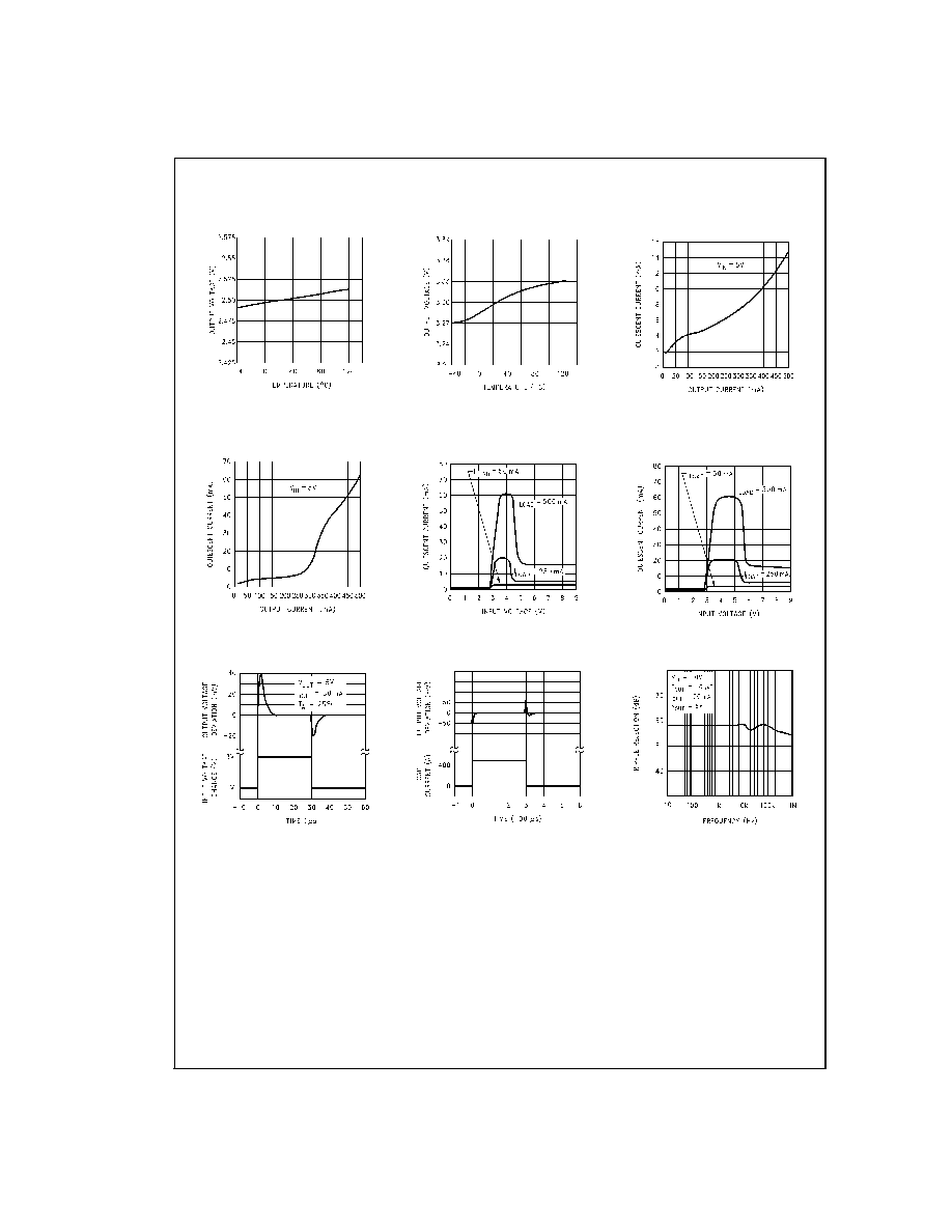
Typical Performance Characteristics
Output Voltage vs
Temperature (2.5V)
DS100113-2
Output Voltage vs
Temperature (3.3V)
DS100113-3
Quiescent Current vs
Output Current (2.5V)
DS100113-4
Quiescent Current vs
Output Current (3.3V)
DS100113-5
Quiescent Current vs
Input Voltage (2.5V)
DS100113-6
Quiescent Current vs
Input Voltage (3.3V)
DS100113-7
Line Transient Response
DS100113-8
Load Transient Response
DS100113-9
Ripple Rejection
DS100113-10
www.national.com
4
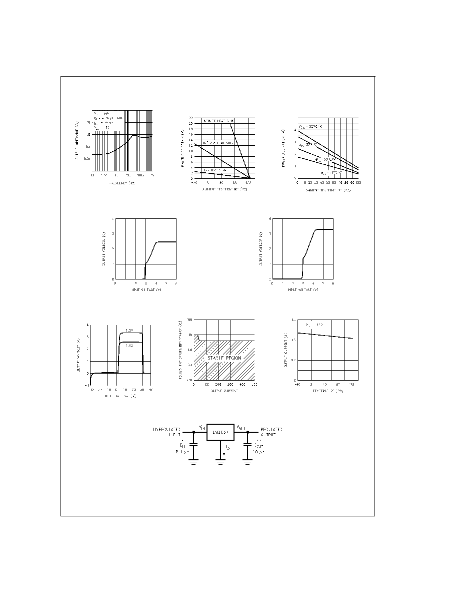
Typical Performance Characteristics
(Continued)
Output Impedance
DS100113-11
Maximum Power
Dissipation (TO-220)
DS100113-12
Maximum Power Dissipation
(TO-263) (Note 2)
DS100113-13
Low Voltage Behavior (2.5V)
DS100113-14
Low Voltage Behavior (3.3)
DS100113-15
Output at Voltage
Extremes
DS100113-16
Output Capacitor ESR
DS100113-17
Peak Output Current
DS100113-18
Typical Application
DS100113-1
* Required if the regulator is located more than 3 inches from the power supply filter capacitors.
*
*
Required for stability. C
out
must be at least 10 µF (over the full expected operating temperature range) and located as close as possible to the regulator. The
equivalent series resistance, ESR, of this capacitor may be as high as 3
.
5
www.national.com