 | –≠–ª–µ–∫—Ç—Ä–æ–Ω–Ω—ã–π –∫–æ–º–ø–æ–Ω–µ–Ω—Ç: LM3526 | –°–∫–∞—á–∞—Ç—å:  PDF PDF  ZIP ZIP |

LM3526
Dual Port USB Power Switch and Over-Current
Protection
General Description
The LM3526 provides Universal Serial Bus standard power
switch and over-current protection for all host port applica-
tions. The dual port device is ideal for Notebook and desktop
PC's that supply power to more than one port.
A 1 ms delay on the fault flag output prevents erroneous
overcurrent reporting caused by in-rush currents during
hot-plug events.
The dual stage thermal protection circuit in the LM3526 pro-
vides individual protection to each switch and the entire de-
vice. In a short-circuit/over-current event, the switch dissipat-
ing excessive heat is turned off, allowing the second switch
to continue to function uninterrupted.
The LM3526 accepts an input voltage between 2.7V and
5.5V allowing use as a device-based in-rush current limiter
for 3.3V USB peripherals, as well as Root and Self-Powered
Hubs at 5.5V. The Enable inputs accept both 3.3V and 5.0V
logic thresholds.
The small size, low R
ON
, and 1 ms fault flag delay make the
LM3526 a good choice for root hubs as well as per-port
power control in embedded and stand-alone hubs.
Features
n
1 ms fault flag delay filters Hot-Plug events
n
Smooth turn-on eliminates in-rush induced voltage drop
n
UL recognized component: REF# 205202
n
1A nominal short circuit output current protects PC
power supplies
n
Thermal shutdown protects device in direct short
condition
n
500mA minimum continuous load current
n
Small SO-8 package minimizes board space
n
2.7V to 5.5V input voltage range
n
140 m
Max. switch resistance
n
1 µA Max. standby current
n
200 µA Max. operating current
n
Under-voltage lockout (UVLO)
Applications
n
Universal Serial Bus (USB) Root Hubs including
Desktop and Notebook PC
n
USB Monitor Hubs
n
Other Self-Powered USB Hub Devices
n
High Power USB Devices Requiring In-rush Limiting
n
General Purpose High Side Switch Applications
Typical Operating Circuit and Connection Diagram
DS101097-1
DS101097-2
LM3526-H
DS101097-40
DS101097-28
LM3526-L
February 2000
LM3526
Dual
Port
USB
Power
Switch
and
Over-Current
Protection
© 2000 National Semiconductor Corporation
DS101097
www.national.com

Ordering Information
Part Number
Enable, Delivery Option
Package Type
LM3526M-H
Active High Enable, 95 units per rail
SO-8,
NS Package
Number M08A
LM3526M-L
Active Low Enable, 95 units per rail
LM3526MX-H
Active High Enable, 2500 units per reel
LM3526MX-L
Active Low Enable, 2500 units per reel
LM3526
www.national.com
2

Absolute Maximum Ratings
(Note 1)
If Military/Aerospace specified devices are required,
please contact the National Semiconductor Sales Office/
Distributors for availability and specifications.
Supply Voltage
-0.3V to 6V
Output Voltage
-0.3V to 6V
Voltage at All Other Pins
-0.3V to 5.5V
Power Dissipation (T
A
= 25∞C)
(Note 2)
700 mW
T
JMAX
(Note 2)
160∞C
Operating Ratings
Supply Voltage Range
2.7V to 5.5V
Operating Ambient Range
-40∞C to 85∞C
Operating Junction Temperature
Range
-40∞C to 125∞C
Storage Temperature Range
-65∞C to +150∞C
Lead Temperature
(Soldering, 5 seconds)
260∞C
ESD Rating (Note 3)
ESD Rating Output Only
2kV
8kV
DC Electrical Characteristics
Limits in standard typeface are for T
J
= 25∞C, and limits in boldface type apply over the full operating temperature range. Un-
less otherwise specified: V
IN
= 5.0V, V
EN
= 0V (LM3526-L) or V
EN
= V
IN
(LM3526-H).
Symbol
Parameter
Conditions
Min
Typ
Max
Units
R
ON
On Resistance
V
IN
= 5V, I
OUT
= 500mA, each switch
100
140
m
V
IN
= 2.7V, I
OUT
= 500mA, each switch
110
180
I
OUT
OUT pins continuous
output current
Each Output
0.5
A
I
SC
Short Circuit Output
Current
Each Output (enable into Load) (Note 4)
V
OUT
= 4.0V
V
OUT
= 0.1V
0.5
1.2
1
1.9
1.5
A
OC
THRESH
Over-current Threshold
2.2
3.2
A
I
LEAK
OUT pins Output
Leakage Current
V
EN
= V
IN
(LM3526-L)
V
EN
= 0V (LM3526-H)
0.01
10
µA
R
FO
FLAG Output Voltage
I
FO
= 10 mA, V
IN
= 5.0V
10
25
I
FO
= 10 mA, V
IN
= 3.3V
11
35
I
FO
= 10 mA, V
IN
= 2.7V
12
40
I
EN
EN/EN Leakage Current
V
EN
/V
EN
= 0V or V
EN
/V
EN
= V
IN
-0.5
0.5
µA
V
IH
EN/EN Input Logic High
(Note 5)
2.4
1.9
V
V
IL
EN/EN Input Logic Low
(Note 5)
1.7
0.8
V
V
UVLO
Under-Voltage Lockout
Threshold
1.8
V
I
DDOFF
Supply Current
Switch-Off
-40∞C
T
J
85∞C
0.2
1
2
µA
I
DDON
Supply Current
Switch-On
115
200
µA
Th
SD
Over-temperature
Shutdown Threshold
T
J
Increasing, with no shorted output
T
J
Increasing, with shorted output (s)
T
J
Decreasing (Note 4)
150
145
135
∞C
I
FH
Error Flag Leakage
Current
V
flag
= 5V
0.01
1
µA
Note 1: Absolute Maximum Ratings indicate limits beyond which damage to the device may occur. Electrical specifications do not apply when operating the device
beyond its rated operating conditions.
Note 2: The maximum power dissipation must be derated at elevated temperatures and is dictated by T
JMAX
(Maximum junction temperature),
JA
(junction to am-
bient thermal resistance), and T
A
(ambient temperature). The maximum allowable power dissipation at any temperature is P
DMAX
= (T
JMAX
- T
A
)/
JA
or the number
given in the Absolute Maximum Ratings, which ever is lower.
JA
= 150∞C/W.
Note 3: The human body model is a 100 pF capacitor discharged through a 1.5 k
resistor into each pin. Enable pin ESD threshold is 1.7kV.
Note 4: Thermal Shutdown will protect the device from permanent damage.
Note 5: For LM3526-L, OFF is EN
2.4V and ON is EN
0.8V. For LM3526-H, OFF is EN
0.8V and ON is EN
2.4V.
LM3526
www.national.com
3
AC Electrical Characteristics
Limits in standard typeface are for T
J
= 25∞C, and limits in boldface type apply over the full operating temperature range. Un-
less otherwise specified: V
IN
= 5.0V.
Symbol
Parameter
Conditions
Min
Typ
Max
Units
t
r
OUT Rise Time
R
L
= 10
100
µs
t
f
OUT Fall Time
R
L
= 10
5
µs
t
ON
Turn on Delay, EN to OUT
R
L
= 10
150
µs
t
OFF
Turn off Delay, EN to OUT
R
L
= 10
5
µs
t
OC
Over Current Flag Delay
R
L
= 0
1
ms
Pin Description
Pin Number
Pin Name
Pin Function
1, 4
ENA, ENB
(LM3526-L)
ENA, ENB
(LM3526-H)
Enable (Input): Logic-compatible enable inputs.
2, 3
FLAG A
FLAG B
Fault Flag (Output): Active-low, open-drain outputs. Indicates overcurrent, UVLO or thermal
shutdown.
*
See application section for more information.
6
GND
Ground
7
IN
Supply Input: This pin is the input to the power switch and the supply voltage for the IC.
8, 5
OUT A
OUT B
Switch Output: These pins are the outputs of the high side switch.
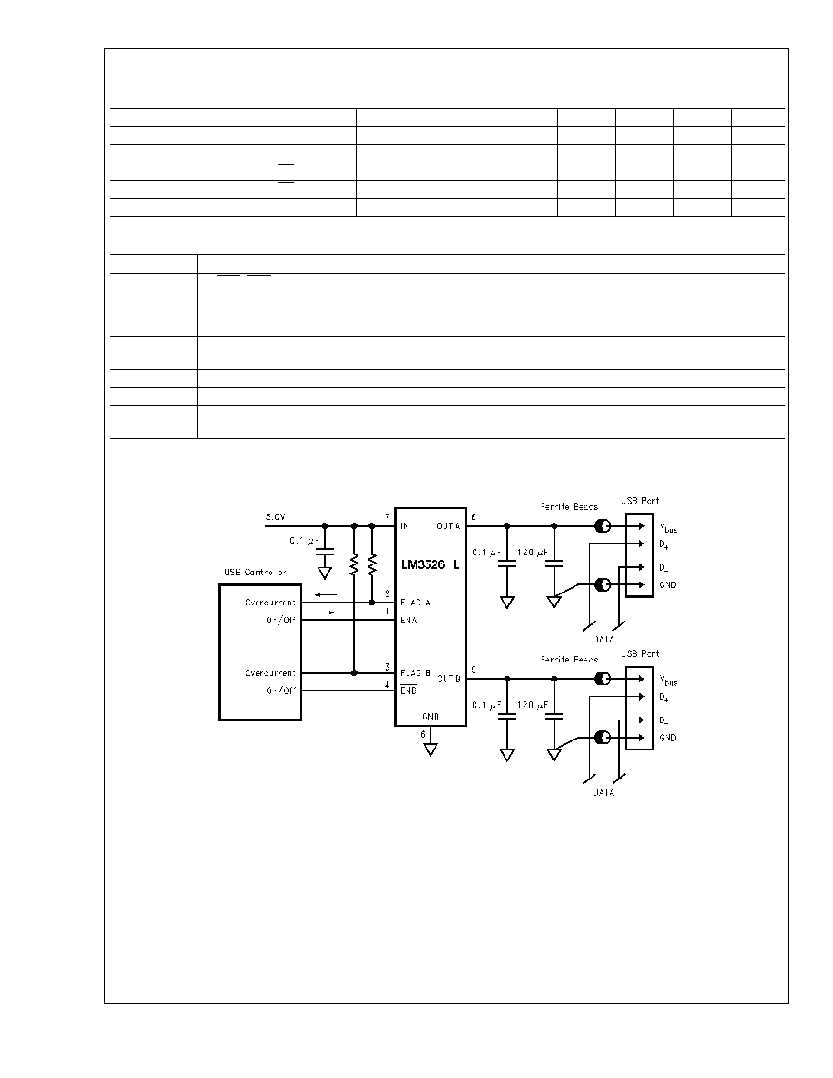
Typical Application Circuit
DS101097-3
LM3526
www.national.com
4

Typical Performance Characteristics
V
IN
= 5.0V, I
L
= 500 mA, T
A
= 25∞C unless otherwise specified.
R
ON
vs Temperature
DS101097-4
R
ON
vs Temperature
DS101097-5
Quiescent Current vs Input Voltage
DS101097-6
Quiescent Current vs Temperature
DS101097-7
Current Limit vs Output Voltage
DS101097-8
OC Threshold vs Temperature
DS101097-9
LM3526
www.national.com
5