
TL H 9241
LM194LM394
Supermatch
Pair
December 1994
LM194 LM394 Supermatch Pair
General Description
The LM194 and LM394 are junction isolated ultra well-
matched monolithic NPN transistor pairs with an order of
magnitude improvement in matching over conventional tran-
sistor pairs This was accomplished by advanced linear pro-
cessing and a unique new device structure
Electrical characteristics of these devices such as drift ver-
sus initial offset voltage noise and the exponential relation-
ship of base-emitter voltage to collector current closely ap-
proach those of a theoretical transistor Extrinsic emitter
and base resistances are much lower than presently avail-
able pairs either monolithic or discrete giving extremely low
noise and theoretical operation over a wide current range
Most parameters are guaranteed over a current range of
1 mA to 1 mA and 0V up to 40V collector-base voltage
ensuring superior performance in nearly all applications
To guarantee long term stability of matching parameters
internal clamp diodes have been added across the emitter-
base junction of each transistor These prevent degradation
due to reverse biased emitter current
the most common
cause of field failures in matched devices The parasitic iso-
lation junction formed by the diodes also clamps the sub-
strate region to the most negative emitter to ensure com-
plete isolation between devices
The LM194 and LM394 will provide a considerable improve-
ment in performance in most applications requiring a closely
matched transistor pair In many cases trimming can be
eliminated entirely
improving reliability and decreasing
costs Additionally the low noise and high gain make this
device attractive even where matching is not critical
The LM194 and LM394 LM394B LM394C are available in
an isolated header 6-lead TO-5 metal can package The
LM394 LM394B LM394C are available in an 8-pin plastic
dual-in-line package The LM194 is identical to the LM394
except for tighter electrical specifications and wider temper-
ature range
Features
Y
Emitter-base voltage matched to 50 mV
Y
Offset voltage drift less than 0 1 mV C
Y
Current gain (h
FE
) matched to 2%
Y
Common-mode rejection ratio greater than 120 dB
Y
Parameters guaranteed over 1 mA to 1 mA collector
current
Y
Extremely low noise
Y
Superior logging characteristics compared to
conventional pairs
Y
Plug-in replacement for presently available devices
Typical Applications
Low Cost Accurate Square Root Circuit
I
OUT
e
10
b
5
0
10 V
IN
TL H 9241 � 1
Low Cost Accurate Squaring Circuit
I
OUT
e
10
b
6
(V
IN
)
2
TL H 9241 � 2
Trim for full scale accuracy
C1995 National Semiconductor Corporation
RRD-B30M115 Printed in U S A

Absolute Maximum Ratings
If Military Aerospace specified devices are required
please contact the National Semiconductor Sales
Office Distributors for availability and specifications
(Note 4)
Collector Current
20 mA
Collector-Emitter Voltage
V
MAX
Collector-Emitter Voltage
35V
LM394C
20V
Collector-Base Voltage
35V
LM394C
20V
Collector-Substrate Voltage
35V
LM394C
20V
Collector-Collector Voltage
35V
LM394C
20V
Base-Emitter Current
g
10 mA
Power Dissipation
500 mW
Junction Temperature
LM194
b
55 C to
a
125 C
LM394 LM394B LM394C
b
25 C to
a
85 C
Storage Temperature Range
b
65 C to
a
150 C
Soldering Information
Metal Can Package (10 sec )
260 C
Dual-In-Line Package (10 sec )
260 C
Small Outline Package
Vapor Phase (60 sec )
215 C
Infrared (15 sec )
220 C
See AN-450 ``Surface Mounting and their Effects on Prod-
uct Reliability'' for other methods of soldering surface
mount devices
Electrical Characteristics
(T
J
e
25 C)
Parameter
Conditions
LM194
LM394
LM394B 394C
Units
Min
Typ
Max
Min
Typ
Max
Min
Typ
Max
Current Gain (h
FE
)
V
CB
e
0V to V
MAX
(Note 1)
I
C
e
1 mA
350
700
300
700
225
500
I
C
e
100 mA
350
550
250
550
200
400
I
C
e
10 mA
300
450
200
450
150
300
I
C
e
1 mA
200
300
150
300
100
200
Current Gain Match
V
CB
e
0V to V
MAX
(h
FE
Match)
I
C
e
10 mA to 1 mA
0 5
2
0 5
4
1 0
5
%
e
100 DI
B
h
FE(MIN)
I
C
I
C
e
1 mA
1 0
1 0
2 0
%
Emitter-Base Offset
V
CB
e
0
25
100
25
150
50
200
m
V
Voltage
I
C
e
1 mA to 1 mA
Change in Emitter-Base
(Note 1)
Offset Voltage vs
I
C
e
1 mA to 1 mA
10
25
10
50
10
100
m
V
Collector-Base Voltage
V
CB
e
0V to V
MAX
(CMRR)
Change in Emitter-Base
V
CB
e
0V
5
25
5
50
5
50
m
V
Offset Voltage vs
I
C
e
1 mA to 0 3 mA
Collector Current
Emitter-Base Offset
I
C
e
10 mA to 1 mA (Note 2)
0 08
0 3
0 08
1 0
0 2
1 5
m
V C
Voltage Temperature
I
C1
e
I
C2
Drift
V
OS
Trimmed to 0 at 25 C
0 03
0 1
0 03
0 3
0 03
0 5
m
V C
Logging Conformity
I
C
e
3 nA to 300 mA
150
150
150
m
V
V
CB
e
0 (Note 3)
Collector-Base Leakage
V
CB
e
V
MAX
0 05
0 25
0 05
0 5
0 05
0 5
nA
Collector-Collector
V
CC
e
V
MAX
0 1
2 0
0 1
5 0
0 1
5 0
nA
Leakage
Input Voltage Noise
I
C
e
100 mA V
CB
e
0V
1 8
1 8
1 8
nV
0
Hz
f
e
100 Hz to 100 kHz
Collector to Emitter
I
C
e
1 mA I
B
e
10 mA
0 2
0 2
0 2
V
Saturation Voltage
I
C
e
1 mA I
B
e
100 mA
0 1
0 1
0 1
V
Note 1
Collector-base voltage is swept from 0 to V
MAX
at a collector current of 1 mA 10 mA 100 mA and 1 mA
Note 2
Offset voltage drift with V
OS
e
0 at T
A
e
25 C is valid only when the ratio of I
C1
to I
C2
is adjusted to give the initial zero offset This ratio must be held to
within 0 003% over the entire temperature range Measurements taken at
a
25 C and temperature extremes
Note 3
Logging conformity is measured by computing the best fit to a true exponential and expressing the error as a base-emitter voltage deviation
Note 4
Refer to RETS194X drawing of military LM194H version for specifications
2
Typical Applications
(Continued)
Fast Accurate Logging Amplifier V
IN
e
10V to 0 1 mV or I
IN
e
1 mA to 10 nA
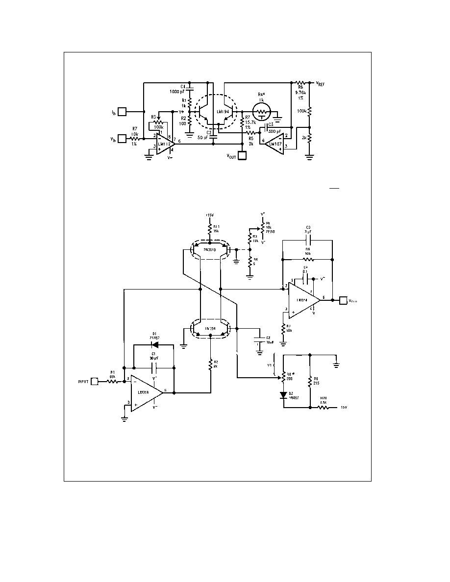
TL H 9241 � 3
1 kX (
g
1%) at 25 C
a
3500 ppm C
Available from Vishay Ultronix
Grand Junction CO Q81 Series
V
OUT
e b
log
10
V
IN
V
REF
J
Voltage Controlled Variable Gain Amplifier
TL H 9241 � 4
R8�R10 and D2 provide a temperature
Distortion
k
0 1%
independent gain control
Bandwidth
l
1 MHz
G
e b
336 V1 (dB)
100 dB gain range
3

Typical Applications
(Continued)
Precision Low Drift Operational Amplifier
Common-mode range 10V
I
BIAS
25 nA
I
OS
0 5 nA
V
OS
(untrimmed) 125 mV
(DV
OS
D
T) 0 2 mV C
CMRR 120 dB
A
VOL
2 500 000
C
200 pF for unity gain
C
30 pF for A
V
10
C
5 pF for A
V
100
TL H 9241 � 5
C
0 pF for A
V
1000
High Accuracy One Quadrant Multiplier Divider
TL H 9241 � 6
V
OUT
e
(X) (Y)
(Z)
positive inputs only
Typical linearity 0 1%
4

Typical Applications
(Continued)
High Performance Instrumentation Amplifier
Gain
e
10
6
R
S
TL H 9241 � 7
Performance Characteristics
G
e
10 000 G
e
1 000 G
e
100 G
e
10
Linearity of Gain (
g
10V Output)
s
0 01
s
0 01
s
0 02
s
0 05
%
Common-Mode Rejection Ratio (60 Hz)
t
120
t
120
t
110
t
90
dB
Common-Mode Rejection Ratio (1 kHz)
t
110
t
110
t
90
t
70
dB
Power Supply Rejection Ratio
a
Supply
l
110
l
110
l
110
l
110
dB
b
Supply
l
110
l
110
l
90
l
70
dB
Bandwidth (
b
3 dB)
50
50
50
50
kHz
Slew Rate
0 3
0 3
0 3
0 3
V ms
Offset Voltage Drift
s
0 25
s
0 4
2
s
10
m
V C
Common-Mode Input Resistance
l
10
9
l
10
9
l
10
9
l
10
9
X
Differential Input Resistance
l
3 x 10
8
l
3 x 10
8 l
3 x 10
8 l
3 x 10
8
X
Input Referred Noise (100 Hz
s
f
s
10 kHz)
5
6
12
70
nV
0Hz
Input Bias Current
75
75
75
75
nA
Input Offset Current
1 5
1 5
1 5
1 5
nA
Common-Mode Range
g
11
g
11
g
11
g
10
V
Output Swing (R
L
e
10 kX)
g
13
g
13
g
13
g
13
V
Assumes
s
5 ppm C tracking of resistors
5