LM4140
High Precision Low Noise Low Dropout Voltage
Reference
General Description
The LM4140 series of precision references are designed to
combine high accuracy, low drift and noise with low power
dissipation in a small package.
The LM4140 is the industry's first reference with output volt-
age options lower than the bandgap voltage.
The key to the advance performance of the LM4140 is the
use of EEPROM registers and CMOS DACs for temperature
coefficient curvature correction and trimming of the output
voltage accuracy of the device during the final production
testing.
The major advantage of this method is the much higher reso-
lution available with DACs than is available economically
with most methods utilized by other bandgap references.
The low input and dropout voltage, low supply current and
output drive capability of the LM4140 makes this product an
ideal choice for battery powered and portable applications.
The LM4140 is available in three grades (A, B, C) with 0.1%
initial accuracy and 3, 6 and 10 ppm/∞C temperature coeffi-
cients. For even lower Tempco, contact National Semicon-
ductor.
The device performance is specified over the temperature
range (0∞C to +70∞C) and is available in compact 8-pin SO
package.
For other output voltage options from 0.5V to 4.5V, con-
tact National Semiconductor.
Features
n
High initial accuracy: 0.1%
n
Ultra low noise
n
Low Temperature Coefficient: 3 ppm/∞C (A grade)
n
Low voltage operation: 1.8V
n
SO-8 package
n
Low dropout voltage: 20 mV (typ)
@
1mA
n
Supply Current: 230 µA (typ),
1 µA disable mode
n
Enable pin
n
Output voltage options: 1.024V, 1.250V, 2.048V, 2.500V,
and 4.096V
n
Custom voltages from 0.5V to 4.5V
n
Temperature range (0∞C to 70∞C)
Applications Summary
n
Portable, battery powered equipment
n
Instrumentation and test equipment
n
Automotive
n
Industrial process control
n
Data acquisition systems
n
Medical equipment
n
Precision scales
n
Servo systems
n
Battery charging
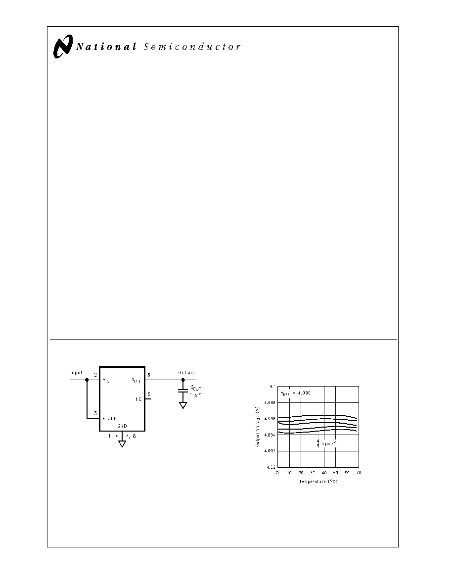
Typical Application
DS101079-1
C
OUT
, Output bypass capacitor. See text for selection detail.
Typical Temperature Coefficient
(Sample of 5 Parts)
DS101079-23
Refer to the Ordering Information Table in this Data Sheet for Specific Part
Number
July 2000
LM4140
High
Precision
Low
Noise
Low
Dropout
V
oltage
Reference
© 2000 National Semiconductor Corporation
DS101079
www.national.com

Ordering Information
Temperature Range (0∞C to 70∞C)
Initial Output Voltage Accuracy
@
25∞C
and Temperature Coefficient
LM4140 Supplied as 95 Units,
Tape and Reel
LM4140 Supplied as 2500
Units, Tape and Reel
0.1%, 3 ppm/∞C max (A grade)
LM4140ACM-1.0
LM4140ACMX-1.0
LM4140ACM-1.2
LM4140ACMX-1.2
LM4140ACM-2.0
LM4140ACMX-2.0
LM4140ACM-2.5
LM4140ACMX-2.5
LM4140ACM-4.1
LM4140ACMX-4.1
0.1%, 6 ppm/∞C max (B grade)
LM4140BCM-1.0
LM4140BCMX-1.0
LM4140BCM-1.2
LM4140BCMX-1.2
LM4140BCM-2.0
LM4140BCMX-2.0
LM4140BCM-2.5
LM4140BCMX-2.5
LM4140BCM-4.1
LM4140BCMX-4.1
0.1%, 10 ppm/∞C max (C grade)
LM4140CCM-1.0
LM4140CCMX-1.0
LM4140CCM-1.2
LM4140CCMX-1.2
LM4140CCM-2.0
LM4140CCMX-2.0
LM4140CCM-2.5
LM4140CCMX-2.5
LM4140CCM-4.1
LM4140CCMX-4.1
Connection Diagram
Pin Functions
V
ref
(Pin 6):
Reference Output. Capable of sourcing up to 8mA.
Input (Pin 2):
Positive Supply.
Ground (Pins 1, 4, 7, 8):
Negative Supply or Ground Connection. These pins must be
connected to ground.
Enable (Pin 3):
Pulled to input for normal operation. Forcing this pin to ground will
turn-off the output.
NC (Pin 5):
This pin must be left open.
8-Lead Surface Mount (M)
DS101079-2
Top View
See NS Package Number M08A
LM4140
www.national.com
2

Absolute Maximum Ratings
(Note 1)
If Military/Aerospace specified devices are required,
please contact the National Semiconductor Sales Office/
Distributors for availability and specifications.
Maximum Voltage on any Input pin
-0.3V to 5.6V
Output Short-Circuit Duration
Indefinite
Power Dissipation (T
A
= 25∞C)
(Note 2)
345mW
ESD Susceptibility (Note 3)
Human Body Model
Machine Model
2 kV
200V
Lead Temperature:
Soldering, (10 sec.)
+260∞C
Operating Range
(Note 1)
Storage Temperature Range
-65∞C to +150∞C
Ambient Temperature Range
0∞C to 70∞C
Junction Temperature Range
0∞C to 80∞C
LM4140
Electrical Charateristics
Unless otherwise specified, V
IN
= 3.0V for the LM4140-1.024 and LM4140-1.250, V
IN
= 5.0V for all other voltage options, V
EN
= V
IN
. C
OUT
= 1µF (Note 4), I
LOAD
= 1mA, T
A
= T
J
= 25∞C. Limits with standard typeface are for T
A
= 25∞C, and limits in
boldface type apply over 0∞C to 70∞C temperature range.
Symbol
Parameter
Conditions
Min
(Note 6)
Typ
(Note 5)
Max
(Note 6)
Units
V
REF
Output Voltage Initial
Accuracy (Note 7)
LM4140B-1.024
LM4140B-1.250
LM4140B-2.048
LM4140B-2.500
LM4140B-4.096
±
0.1
%
LM4140C-1.024
LM4140C-1.250
LM4140C-2.048
LM4140C-2.500
LM4140C-4.096
±
0.1
TCV
REF
/∞C
Temperature Coefficient:
A Grade
B Grade
C Grade
0∞C
T
A
+ 70∞C
3
6
10
ppm/∞C
V
REF
/
V
IN
Line Regulation
ppm/V
1.024V and 1.250V options
1.8V
V
IN
5.5V
50
300
350
All other voltage options
V
ref
+ 200mV
V
IN
5.5V
20
200
250
V
REF
/
I
LOAD
Load Regulation
1 mA
I
LOAD
8mA
ppm/mA
All other voltage options
1
20
150
4.096V Option
5
35
150
V
REF
Long-Term Stability
1000 Hrs
60
ppm
V
REF
Thermal Hysteresis (Note
8)
0∞C
T
A
+ 70∞C
20
ppm
LM4140
www.national.com
3

LM4140
Electrical Charateristics
(Continued)
Unless otherwise specified, V
IN
= 3.0V for the LM4140-1.024 and LM4140-1.250, V
IN
= 5.0V for all other voltage options, V
EN
= V
IN
. C
OUT
= 1µF (Note 4), I
LOAD
= 1mA, T
A
= T
J
= 25∞C. Limits with standard typeface are for T
A
= 25∞C, and limits in
boldface type apply over 0∞C to 70∞C temperature range.
Symbol
Parameter
Conditions
Min
(Note 6)
Typ
(Note 5)
Max
(Note 6)
Units
Operating
Voltage
LM4140-1.024,
LM4140-1.250
I
L
= 1 mA to 8 mA
1.8
5.5
V
V
IN
-V
REF
Dropout Voltage (Note 9)
LM4140-2.048,
LM4140-2.500
I
L
= 1 mA
20
40
45
mV
I
L
= 8 mA
160
235
400
LM4140-4.096
I
L
= 1 mA
20
40
45
I
L
= 8 mA
195
270
490
V
N
Output Noise Voltage
(Note 10)
0.1 Hz to 10 Hz
2.2
µV
PP
I
S(ON)
Supply Current
I
LOAD
= 0 mA
µA
All other voltage options
230
320
375
4.096V Option
265
350
400
I
S(OFF)
Supply Current
V
Enable
<
0.4V
.01
1
µA
V
H
Logic High Input Voltage
0.8V
IN
V
I
H
Logic High Input Current
2
nA
V
L
Logic Low Input Voltage
0.4
V
I
L
Logic Low Input Current
1
nA
I
SC
Short Circuit Current
8.5
20
35
40
mA
Note 1: Absolute Maximum Ratings indicate limits beyond which damage to the device may occur. Operating Ratings indicate conditions for which the device is in-
tended to be functional, but do not guarantee specific performance limits. For guaranteed specifications and test conditions, see Electrical Characteristics. The guar-
anteed specifications apply only for the test conditions listed. Some performance characteristics may degrade when the device is not operated under the listed test
conditions.
Note 2: Without PCB copper enhancements. The maximum power dissipation must be de-rated at elevated temperatures and is limited by T
JMAX
(maximum junction
temperature),
J-A
(junction to ambient thermal resistance) and T
A
(ambient temperature). The maximum power dissipation at any temperature is: PDiss
MAX
= (T
JMAX
- T
A
)/
J-A
up to the value listed in the Absolute Maximum Ratings. The
J-A
for the SO-8 package is 160∞C/W.
Note 3: The human body model is a 100 pF capacitor discharged through a 1.5 k
resistor into each pin. The machine model is a 200 pF capacitor discharged di-
rectly into each pin.
Note 4: For proper operation, a 1µF capacitor is required between the output pin and the GND pin of the device. (See Application Section for details)
Note 5: Typical numbers are at 25∞C and represent the most likely parametric norm.
Note 6: Limits are 100% production tested at 25∞C. Limits over the operating temperature range are guaranteed through correlation using Statistical Quality Control
(SQC) methods. The limits are used to calculate National's Average Outgoing Quality Level (AOQL).
Note 7: High temperature and mechanical stress associated with PCB assembly can have significant impact on the initial accuracy of the LM4140 and may create
significant shifts in V
REF
. See Application Hints section regarding accuracy and PCB layout consideration.
Note 8: Thermal hysteresis is defined as the changes in +25∞C output voltage before and after the cycling of the device from 0∞C to 70∞C.
Note 9: Dropout voltage is defined as the minimum input to output differential voltage at which the output voltage drops by 0.5% below the value measured with V
IN
= 3.0V for the LM4140-1.024 and LM4140-1.250, V
IN
= 5.0V for all other voltage options.
Note 10: The output noise is based on 1.024V option. Output noise is linearly proportional to V
REF
.
LM4140
www.national.com
4

LM4140 Typical Performance Characteristics
Unless otherwise specified, T
A
= 25∞C, No Load,
C
OUT
= 1µF, V
IN
= 3.0V for LM4140-1.024 and LM4140-1.250, and 5V for all other voltage options. V
IN
= V
EN
.
Power Up/Down Ground Current
DS101079-5
Enable Response
DS101079-6
*
The 1µF output capacitor is actively discharged to ground. See ON/OFF Operation section for more details.
Line Transient Response
DS101079-7
Load Transient Response
DS101079-8
LM4140
www.national.com
5