 | –≠–ª–µ–∫—Ç—Ä–æ–Ω–Ω—ã–π –∫–æ–º–ø–æ–Ω–µ–Ω—Ç: LM6182AIN | –°–∫–∞—á–∞—Ç—å:  PDF PDF  ZIP ZIP |
LM6182
Dual 100 mA Output, 100 MHz Current Feedback
Amplifier
General Description
The LM6182 dual current feedback amplifier offers an unpar-
alleled combination of bandwidth, slew-rate, and output cur-
rent. Each amplifier can directly drive a 2V signal into a 50
or 75
back-terminated coax cable system over the full in-
dustrial temperature range. This represents a radical en-
hancement in output drive capability for a dual 8-pin
high-speed amplifier making it ideal for video applications.
Built on National's advanced high-speed VIP II
TM
(Vertically
Integrated
PNP)
process,
the
LM6182
employs
current-feedback providing bandwidth that does not vary
dramatically with gain; 100 MHz at Av = -1, 60 MHz at Av =
-10. With a slew rate of 2000 V/µsec, 2nd harmonic distor-
tion of -50 dBc at 10 MHz and settling time of 50 ns (0.1%),
the two independent amplifiers of the LM6182 offer perfor-
mance that is ideal for data acquisition, high-speed ATE, and
precision pulse amplifier applications.
See the LM6181 data sheet for a single amplifier with these
same features.
Features
(Typical unless otherwise noted)
n
Slew Rate:
2000 V/µs
n
Closed Loop Bandwidth:
100 MHz
n
Settling Time (0.1%):
50 ns
n
Low Differential Gain and Phase Error:
0.05%, 0.04∞
R
L
= 150
n
Low Offset Voltage:
2 mV
n
High Output Drive:
±
10V into 150
n
Characterized for Supply Ranges:
±
5V and
±
15V
n
Improved Performance over OP260 and LT1229
Applications
n
Coax Cable Driver
n
Professional Studio Video Equipment
n
Flash ADC Buffer
n
PC and Workstation Video Boards
n
Facsimile and Imaging Systems
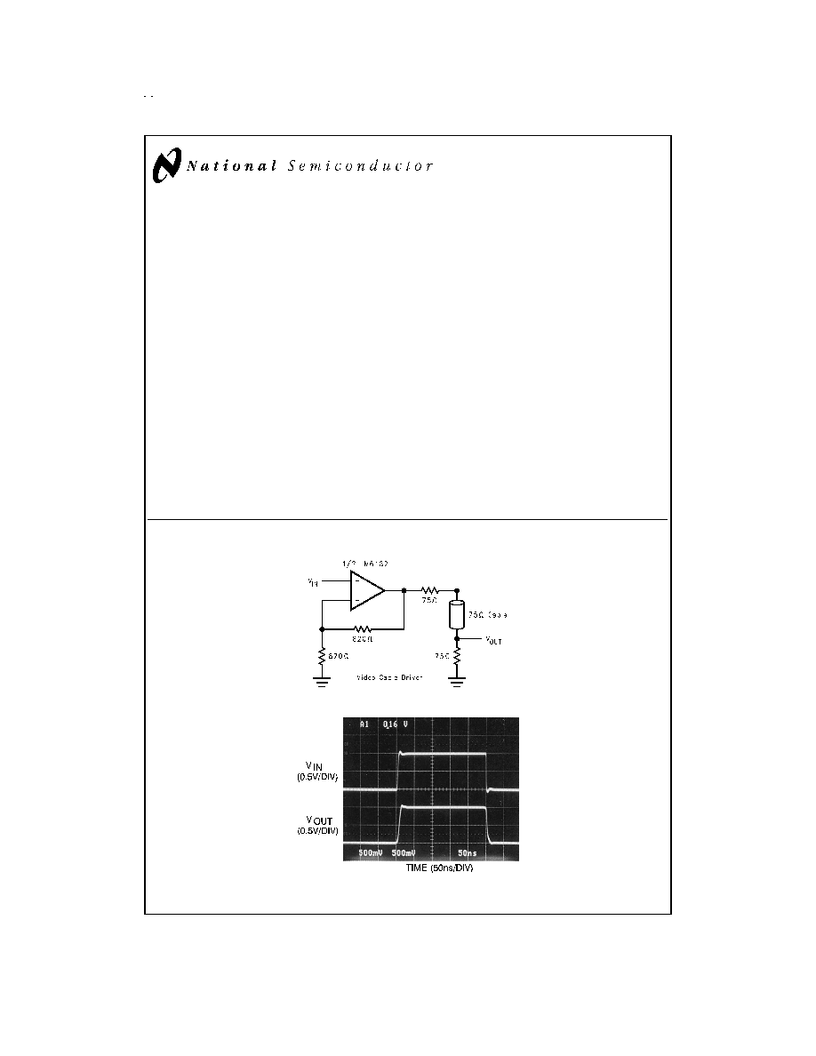
Typical Application
VIP II
TM
is a trademark of National Semiconductor Corporation.
DS011926-1
DS011926-2
April 1994
LM6182
Dual
100
mA
Output,
100
MHz
Current
Feedback
Amplifier
© 1999 National Semiconductor Corporation
DS011926
www.national.com

Connection Diagrams
Dual-In-Line Package (J)
DS011926-51
Order Number LM6182AMJ/883
See NS Package Number J14A
Small Outline Package (M)
DS011926-4
*
Heat Sinking Pins (Note 3)
Order Number LM6182IM or LM6182AIM
See NS Package Number M16A
Dual-In-Line Package (N)
DS011926-3
Order Number LM6182IN, LM6182AIN or LM6182AMN
See NS Package Number N08E
www.national.com
2
Absolute Maximum Ratings
(Note 1)
If Military/Aerospace specified devices are required,
please contact the National Semiconductor Sales Office/
Distributors for availability and specifications.
Supply Voltage
±
18V
Differential Input Voltage
±
6V
Input Voltage
±
Supply Voltage
Inverting Input Current
15 mA
Output Short Circuit
(Note 4)
Soldering Information
Dual-In-Line Package (N)
Soldering (10s)
260∞C
Small Outline Package (M)
Vapor Phase (60s)
215∞C
Infrared (15s)
220∞C
Storage Temperature Range
-65∞C
T
J
+150∞C
Junction Temperature
150∞C
ESD Rating (Note 2)
±
2000V
Operating Ratings
Supply Voltage Range
7V to 32V
Junction Temperature Range (Note 3)
LM6182AM
-55∞C
T
J
+125∞C
LM6182AI, LM6182I
-40∞C
T
J
+85∞C
±
15V DC Electrical Characteristics
The following specifications apply for supply voltage =
±
15V, Vcm = V
O
= 0V, R
f
= 820
, and R
L
= 1 k
unless otherwise
noted. Boldface limits apply at the temperature extremes; all other limits T
J
= 25∞C.
Symbol
Parameter
Conditions
Typical
(Note 5)
LM6182AM LM6182AI
LM6182I
Units
Limit
Limit
Limit
(Note 6)
(Note 6)
(Note 6)
V
OS
Input Offset Voltage
2.0
3.0
3.0
5.0
mV
4.0
3.5
5.5
max
TCV
OS
Input Offset Voltage Drift
5.0
µV/∞C
I
B
Inverting Input Bias Current
2.0
5.0
5.0
10.0
µA
max
12.0
12.0
17.0
Non-Inverting Input Bias Current
0.75
2.0
2.0
3.0
4.0
4.0
5.0
TCI
B
Inverting Input Bias Current Drift
30
nA/∞C
Non-Inverting Input Bias Current Drift
10
I
B
Inverting Input Bias Current
±
4.5V
V
S
±
16V
0.1
0.5
0.5
0.75
µA/V
max
PSR
Power Supply Rejection
3.0
3.0
4.5
Non-Inverting Input Bias Current
±
4.5V
V
S
±
16V
0.05
0.5
0.5
0.5
Power Supply Rejection
1.5
1.5
3.0
I
B
Inverting Input Bias Current
-10V
V
CM
+10V
0.15
0.5
0.5
0.75
CMR
Common Mode Rejection
1.0
1.0
1.5
Non-Inverting Input Bias Current
-10V
V
CM
+10V
0.1
0.5
0.5
0.5
Common Mode Rejection
1.0
1.0
1.5
CMRR
Common Mode Rejection Ratio
-10V
V
CM
+10V
60
50
50
50
dB
47
47
47
min
PSRR
Power Supply Rejection Ratio
±
4.5V
V
S
±
16V
80
70
70
70
dB
67
67
65
min
R
O
Output Resistance
A
V
= -1
0.2
f = 300 kHz
R
IN
Non-Inverting Input Resistance
10
M
V
O
Output Voltage Swing
R
L
= 1 k
12
11
11
11
V
min
10
10
10
R
L
= 150
11
9.5
9.5
9.5
5.6
6.0
6.0
I
SC
Output Short Circuit Current
100
70
70
70
mA
37.5
40
40
min
www.national.com
3
±
15V DC Electrical Characteristics
(Continued)
The following specifications apply for supply voltage =
±
15V, Vcm = V
O
= 0V, R
f
= 820
, and R
L
= 1 k
unless otherwise
noted. Boldface limits apply at the temperature extremes; all other limits T
J
= 25∞C.
Symbol
Parameter
Conditions
Typical
(Note 5)
LM6182AM LM6182AI
LM6182I
Units
Limit
Limit
Limit
(Note 6)
(Note 6)
(Note 6)
Z
T
Transimpedance
R
L
= 1 k
1.8
1.0
1.0
0.8
M
min
0.4
0.5
0.4
R
L
= 150
1.4
0.8
0.8
0.7
0.3
0.35
0.3
I
S
Supply Current
No Load, V
IN
= 0V
15
20
20
20
mA
Both Amplifiers
22
22
22
max
V
CM
Input Common Mode Voltage Range
V
+
-1.7V
V
V
-
+1.7V
±
15V AC Electrical Characteristics
The following specifications apply for supply voltage =
±
15V, Vcm = V
O
= 0V, R
f
= 820
, and R
L
= 1 k
unless otherwise
noted. Boldface limits apply at the temperature extremes; all other limits T
J
= 25∞C.
Symbol
Parameter
Conditions
Typical
(Note 5)
LM6182AM LM6182AI
LM6182I
Units
Limit
Limit
Limit
(Note 6)
(Note 6)
(Note 6)
Xt
Crosstalk Rejection
(Note 7)
93
dB
BW
Closed Loop Bandwidth -3 dB
A
V
= +2
100
MHz
A
V
= +10
75
A
V
= -1
100
A
V
= -10
60
Closed Loop Bandwidth
A
V
= +2, R
L
= 150
35
0.1 dB Flat, R
SOURCE
= 200
PBW
Power Bandwidth
A
V
= -1, V
O
= 5 V
PP
60
SR
Slew Rate
Overdriven
2000
V/µs
min
A
V
= -1, V
O
=
±
10V
1400
1000
1000
1000
R
L
= 150
, (Note 8)
t
s
Settling Time (0.1%)
A
V
= -1, V
O
=
±
5V
50
ns
R
L
= 150
t
r
, t
f
Rise and Fall Time
V
O
= 1 V
PP
5
t
p
Propagation Delay Time
V
O
= 1 V
PP
6
in(+)
Non-Inverting Input Noise
Current Density
f = 1 kHz
3
pA/
Hz
in(-)
Inverting Input Noise
Current Density
f = 1 kHz
16
pA/
Hz
e
n
Input Noise Voltage Density
f = 1 kHz
4
nV/
Hz
Second Harmonic Distortion
V
O
= 2 V
PP
, f = 10 MHz
-50
dBc
A
V
= +2
Third Harmonic Distortion
V
O
= 2 V
PP
, f = 10 MHz
-55
A
V
= +2
Differential Gain
R
L
= 150
0.05
%
A
V
= +2, NTSC
Differential Phase
R
L
= 150
0.04
Deg
A
V
= +2, NTSC
THD
Total Harmonic Distortion
V
O
= 2 V
PP
, A
V
= +2,
0.58
%
f = 10 MHz, R
L
= 150
www.national.com
4
±
5V DC Electrical Characteristics
The following specifications apply for supply voltage =
±
5V, Vcm = V
O
= 0V, R
f
= 820
, and R
L
= 1 k
unless otherwise
noted. Boldface limits apply at the temperature extremes; all other limits T
J
= 25∞C.
Symbol
Parameter
Conditions
Typical
(Note 5)
LM6182AM LM6182AI
LM6182I
Units
Limit
Limit
Limit
(Note 6)
(Note 6)
(Note 6)
V
OS
Input Offset Voltage
1.0
2.0
2.0
3.0
mV
3.0
2.5
3.5
max
TCV
OS
Input Offset Voltage Drift
2.5
µV/∞C
I
B
Inverting Input Bias Current
5.0
10
10
17.5
µA
max
22
22
27.0
Non-Inverting Input Bias Current
0.25
1.5
1.5
3.0
3.0
3.0
5.0
TCI
B
Inverting Input Bias Current Drift
50
nA/∞C
Non-Inverting Input Bias Current Drift
3.0
I
B
Inverting Input Bias Current
±
4V
V
S
±
6V
0.3
0.5
0.5
0.75
µA/V
max
PSR
Power Supply Rejection
1.0
1.0
1.5
Non-Inverting Input Bias Current
±
4V
V
S
±
6V
0.05
0.5
0.5
0.5
Power Supply Rejection
1.0
1.0
1.5
I
B
Inverting Input Bias Current
-2.5V
V
CM
+2.5V
0.3
0.5
0.5
1.0
CMR
Common Mode Rejection
1.0
1.0
1.5
Non-Inverting Input Bias Current
-2.5V
V
CM
+2.5V
0.12
0.5
0.5
0.5
Common Mode Rejection
1.0
1.0
1.5
CMRR
Common Mode Rejection Ratio
-2.5V
V
CM
+2.5V
57
50
50
50
dB
min
47
47
47
PSRR
Power Supply Rejection Ratio
±
4V
V
S
±
6V
80
70
70
64
67
67
60
R
O
Output Resistance
A
V
= -1
0.25
f = 300 kHz
R
IN
Non-Inverting Input Resistance
8
M
V
O
Output Voltage Swing
R
L
= 1 k
2.6
2.25
2.25
2.25
V
min
2.0
2.0
2.0
R
L
= 150
2.2
2.0
2.0
2.0
1.8
1.8
1.8
I
SC
Output Short Circuit Current
100
65
65
65
mA
35
40
40
min
Z
T
Transimpedance
R
L
= 1 k
1.4
0.75
0.75
0.6
M
min
0.3
0.35
0.3
R
L
= 150
1.0
0.5
0.5
0.4
0.2
0.25
0.2
I
S
Supply Current
No Load, V
IN
= 0V
13
17
17
17
mA
Both Amplifiers
18.5
18.5
18.5
max
V
CM
Input Common Mode Voltage Range
V
+
-1.7V
V
V
-
+1.7V
www.national.com
5