 | –≠–ª–µ–∫—Ç—Ä–æ–Ω–Ω—ã–π –∫–æ–º–ø–æ–Ω–µ–Ω—Ç: LM7121IM5 | –°–∫–∞—á–∞—Ç—å:  PDF PDF  ZIP ZIP |

LM7121
235 MHz Tiny Low Power Voltage Feedback Amplifier
General Description
The LM7121 is a high performance operational amplifier
which addresses the increasing AC performance needs of
video and imaging applications, and the size and power con-
straints of portable applications.
The LM7121 can operate over a wide dynamic range of sup-
ply voltages, from 5V (single supply) up to
±
15V (see the Ap-
plication Information section for more details). It offers an ex-
cellent speed-power product delivering 1300V/µs and 235
MHz Bandwidth (-3 dB, A
V
= +1). Another key feature of this
operational amplifier is stability while driving unlimited ca-
pacitive loads.
Due to its Tiny SOT23-5 package, the LM7121 is ideal for
designs where space and weight are the critical parameters.
The benefits of the Tiny package are evident in small por-
table electronic devices, such as cameras, and PC video
cards. Tiny amplifiers are so small that they can be placed
anywhere on a board close to the signal source or near the
input to an A/D converter.
Features
(Typical unless otherwise noted) V
S
=
±
15V
n
Easy to use voltage feedback topology
n
Stable with unlimited capacitive loads
n
Tiny SOT23-5 package -- typical circuit layout takes half
the space of SO-8 designs
n
Unity gain frequency:
175 MHz
n
Bandwidth (-3 dB, A
V
= +1, R
L
= 100
):
235 MHz
n
Slew rate:
1300V/µs
n
Supply Voltages SO-8:
5V to
±
15V
SOT23-5:
5V to
±
5V
n
Characterized for:
+5V,
±
5V,
±
15V
n
Low supply current:
5.3 mA
Applications
n
Scanners, color fax, digital copiers
n
PC video cards
n
Cable drivers
n
Digital cameras
n
ADC/DAC buffers
n
Set-top boxes
Connection Diagrams
Ordering Information
Package
Ordering Information
NSC Drawing
Package
Supplied As
Number
Marking
8-Pin SO-8
LM7121IM
M08A
LM7121IM
Rails
LM7121IMX
M08A
LM7121IM
2.5k Tape and Reel
5-Pin SOT23-5
LM7121IM5
MA05A
A03A
1k Tape and Reel
LM7121IM5X
MA05A
A03A
3k Tape and Reel
8-Pin SO-8
DS012348-2
Top View
5-Pin SOT23
DS012348-1
Top View
August 1999
LM7121
235
MHz
T
iny
Low
Power
V
oltage
Feedback
Amplifier
© 1999 National Semiconductor Corporation
DS012348
www.national.com

Absolute Maximum Ratings
(Note 1)
If Military/Aerospace specified devices are required,
please contact the National Semiconductor Sales Office/
Distributors for availability and specifications.
ESD Tolerance (Note 2)
2000V
Differential Input Voltage (Note 7)
±
2V
Voltage at Input/Output Pin
(V
+
)-1.4V, (V
-
)+1.4V
Supply Voltage (V
+
≠V
-
)
36V
Output Short Circuit to Ground
(Note 3)
Continuous
Lead Temperature
260∞C
(soldering, 10 sec)
260∞C
Storage Temperature Range
-65∞C to +150∞C
Junction Temperature (Note 4)
150∞C
Operating Ratings
(Note 1)
Supply Voltage: SO-8
4.5V
V
S
33V
SOT23-5
4.5V
V
S
11V
Junction Temperature Range
-40∞C
T
J
+85∞C
Thermal Resistance (
JA
)
M Package, 8-pin Surface Mount
165∞C/W
SOT23-5 Package
325∞C/W
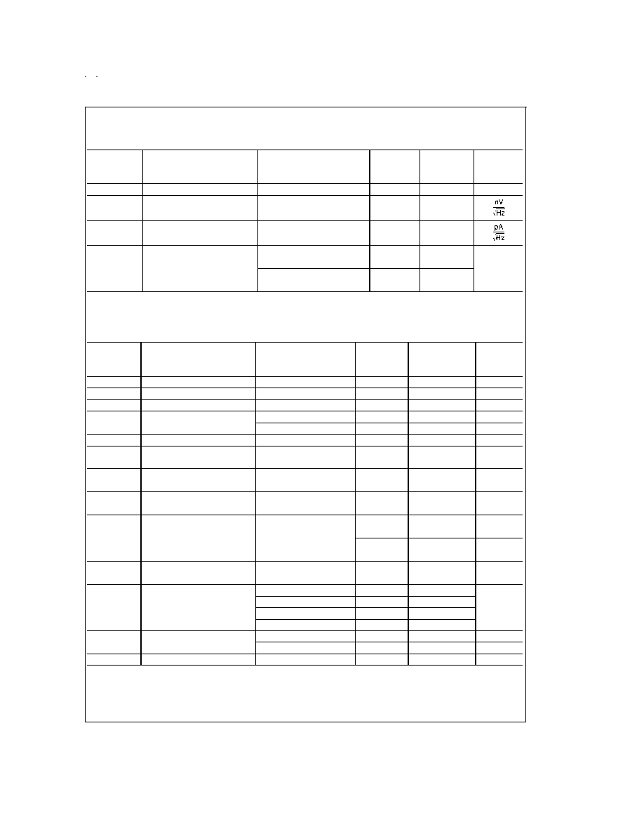
±
15V DC Electrical Characteristics
Unless otherwise specified, all limits guaranteed for T
J
= 25∞C, V
+
= +15V, V
-
= -15V, V
CM
= V
O
= 0V and R
L
>
1 M
.
Boldface limits apply at the temperature extremes.
Symbol
Parameter
Conditions
Typ
(Note 5)
LM7121I
Units
Limit
(Note 6)
V
OS
Input Offset Voltage
0.9
8
mV
15
max
I
B
Input Bias Current
5.2
9.5
µA
12
max
I
OS
Input Offset Current
0.04
4.3
µA
7
max
R
IN
Input Resistance
Common Mode
10
M
Differential Mode
3.4
M
C
IN
Input Capacitance
Common Mode
2.3
pF
CMRR
Common Mode
-10V
V
CM
10V
93
73
dB
Rejection Ratio
70
min
+PSRR
Positive Power Supply
10V
V
+
15V
86
70
dB
Rejection Ratio
68
min
-PSRR
Negative Power Supply
-15V
V
-
-10V
81
68
dB
Rejection Ratio
65
min
V
CM
Input Common-Mode
CMRR
70 dB
13
11
V
Voltage Range
min
-13
-11
V
max
A
V
Large Signal
R
L
= 2 k
, V
O
= 20 V
PP
72
65
dB
Voltage Gain
57
min
V
O
Output Swing
R
L
= 2 k
13.4
11.1
V
10.8
min
-13.4
-11.2
V
-11.0
max
R
L
= 150
10.2
7.75
V
7.0
min
-7.0
-5.0
V
-4.8
max
I
SC
Output Short Circuit
Sourcing
71
54
mA
Current
44
min
Sinking
52
39
mA
34
min
www.national.com
2

±
15V DC Electrical Characteristics
(Continued)
Unless otherwise specified, all limits guaranteed for T
J
= 25∞C, V
+
= +15V, V
-
= -15V, V
CM
= V
O
= 0V and R
L
>
1 M
.
Boldface limits apply at the temperature extremes.
Symbol
Parameter
Conditions
Typ
(Note 5)
LM7121I
Units
Limit
(Note 6)
I
S
Supply Current
5.3
6.6
mA
7.5
max
±
15V AC Electrical Characteristics
Unless otherwise specified, all limits guaranteed for T
J
= 25∞C, V
+
= 15V, V
-
= -15V, V
CM
= V
O
= 0V and R
L
>
1 M
. Bold-
face limits apply at the temperature extremes.
Symbol
Parameter
Conditions
Typ
(Note 5)
LM7121I
Units
Limit
(Note 6)
SR
Slew Rate
A
V
= +2, R
L
= 1 k
,
1300
V/µs
(Note 8)
V
O
= 20 V
PP
GBW
Unity Gain-Bandwidth
R
L
= 1 k
175
MHz
m
Phase Margin
63
Deg
f (-3 dB)
Bandwidth
R
L
= 100
, A
V
= +1
235
MHz
(Notes 9, 10)
R
L
= 100
, A
V
= +2
50
t
s
Settling Time
10 V
PP
Step, to 0.1%,
74
ns
R
L
= 500
t
r
, t
f
Rise and Fall Time
A
V
= +2, R
L
= 100
,
5.3
ns
(Note 10)
V
O
= 0.4 V
PP
A
D
Differential Gain
A
V
= +2, R
L
= 150
0.3
%
D
Differential Phase
A
V
= +2, R
L
= 150
0.65
Deg
e
n
Input-Referred
f = 10 kHz
17
Voltage Noise
i
n
Input-Referred
f = 10 kHz
1.9
Current Noise
T.H.D.
Total Harmonic Distortion
2 V
PP
Output, R
L
= 150
,
0.065
%
A
V
= +2, f = 1 MHz
2 V
PP
Output, R
L
= 150
,
0.52
A
V
= +2, f = 5 MHz
±
5V DC Electrical Characteristics
Unless otherwise specified, all limits guaranteed for T
J
= 25∞C, V
+
= 5V, V
-
= -5V, V
CM
= V
O
= 0V and R
L
>
1 M
. Bold-
face limits apply at the temperature extremes.
Symbol
Parameter
Conditions
Typ
(Note 5)
LM7121I
Units
Limit
(Note 6)
V
OS
Input Offset Voltage
1.6
8
mV
15
max
I
B
Input Bias Current
5.5
9.5
µA
12
max
I
OS
Input Offset Current
0.07
4.3
µA
7.0
max
R
IN
Input Resistance
Common Mode
6.8
M
Differential Mode
3.4
M
www.national.com
3

±
5V DC Electrical Characteristics
(Continued)
Unless otherwise specified, all limits guaranteed for T
J
= 25∞C, V
+
= 5V, V
-
= -5V, V
CM
= V
O
= 0V and R
L
>
1 M
. Bold-
face limits apply at the temperature extremes.
Symbol
Parameter
Conditions
Typ
(Note 5)
LM7121I
Units
Limit
(Note 6)
C
IN
Input Capacitance
Common Mode
2.3
pF
CMRR
Common Mode
-2V
V
CM
2V
75
65
dB
Rejection Ratio
60
min
+PSRR
Positive Power Supply
3V
V
+
5V
89
65
dB
Rejection Ratio
60
min
-PSRR
Negative Power Supply
-5V
V
-
-3V
78
65
dB
Rejection Ratio
60
min
V
CM
Input Common Mode
CMRR
60 dB
3
2.5
V
Voltage Range
min
-3
-2.5
V
max
A
V
Large Signal
R
L
= 2 k
, V
O
= 3 V
PP
66
60
dB
Voltage Gain
58
min
V
O
Output Swing
R
L
= 2 k
3.62
3.0
V
2.75
min
-3.62
-3.0
V
-2.70
max
R
L
= 150
3.1
2.5
V
2.3
min
-2.8
-2.15
V
-2.00
max
I
SC
Output Short Circuit
Sourcing
53
38
mA
Current
33
min
Sinking
29
21
mA
19
min
I
S
Supply Current
5.1
6.4
mA
7.2
max
±
5V AC Electrical Characteristics
Unless otherwise specified, all limits guaranteed for T
J
= 25∞C, V
+
= 5V, V
-
= -5V, V
CM
= V
O
= 0V and R
L
>
1 M
. Bold-
face limits apply at the temperature extremes.
Symbol
Parameter
Conditions
Typ
(Note 5)
LM7121I
Units
Limit
(Note 6)
SR
Slew Rate
A
V
= +2, R
L
= 1 k
,
520
V/µs
(Note 8)
V
O
= 6 V
PP
GBW
Unity Gain-Bandwidth
R
L
= 1 k
105
MHz
m
Phase Margin
R
L
= 1 k
74
Deg
f (-3 dB)
Bandwidth
R
L
= 100
, A
V
= +1
160
MHz
(Notes 9, 10)
R
L
= 100
, A
V
= +2
50
t
s
Settling Time
5 V
PP
Step, to 0.1%,
65
ns
R
L
= 500
t
r
, t
f
Rise and Fall Time
A
V
= +2, R
L
= 100
,
5.8
ns
(Note 10)
V
O
= 0.4 V
PP
A
D
Differential Gain
A
V
= +2, R
L
= 150
0.3
%
www.national.com
4
±
5V AC Electrical Characteristics
(Continued)
Unless otherwise specified, all limits guaranteed for T
J
= 25∞C, V
+
= 5V, V
-
= -5V, V
CM
= V
O
= 0V and R
L
>
1 M
. Bold-
face limits apply at the temperature extremes.
Symbol
Parameter
Conditions
Typ
(Note 5)
LM7121I
Units
Limit
(Note 6)
D
Differential Phase
A
V
= +2, R
L
= 150
0.65
Deg
e
n
Input-Referred
f = 10 kHz
17
Voltage Noise
i
n
Input-Referred
f = 10 kHz
2
Current Noise
T.H.D.
Total Harmonic Distortion
2 V
PP
Output, R
L
= 150
,
0.1
%
A
V
= +2, f = 1 MHz
2 V
PP
Output, R
L
= 150
,
0.6
A
V
= +2, f = 5 MHz
+5V DC Electrical Characteristics
Unless otherwise specified, all limits guaranteed for T
J
= 25∞C, V
+
= +5V, V
-
= 0V, V
CM
= V
O
= V
+
/2 and R
L
>
1 M
. Bold-
face limits apply at the temperature extremes.
Symbol
Parameter
Conditions
Typ
(Note 5)
LM7121I
Units
Limit
(Note 6)
V
OS
Input Offset Voltage
2.4
mV
I
B
Input Bias Current
4
µA
I
OS
Input Offset Current
0.04
µA
R
IN
Input Resistance
Common Mode
2.6
M
Differential Mode
3.4
M
C
IN
Input Capacitance
Common Mode
2.3
pF
CMRR
Common Mode
2V
V
CM
3V
65
dB
Rejection Ratio
+PSRR
Positive Power Supply
4.6V
V
+
5V
85
dB
Rejection Ratio
-PSRR
Negative Power Supply
0V
V
-
0.4V
61
dB
Rejection Ratio
V
CM
Input Common-Mode
CMRR
45 dB
3.5
V
Voltage Range
min
1.5
V
max
A
V
Large Signal
R
L
= 2 k
to V
+
/2
64
dB
Voltage Gain
V
O
Output Swing
R
L
= 2 k
to V
+
/2, High
3.7
V
R
L
= 2 k
to V
+
/2, Low
1.3
R
L
= 150
to V
+
/2, High
3.48
R
L
= 150
to V
+
/2, Low
1.59
I
SC
Output Short Circuit
Sourcing
33
mA
Current
Sinking
20
mA
I
S
Supply Current
4.8
mA
www.national.com
5