 | –≠–ª–µ–∫—Ç—Ä–æ–Ω–Ω—ã–π –∫–æ–º–ø–æ–Ω–µ–Ω—Ç: LM828M5 | –°–∫–∞—á–∞—Ç—å:  PDF PDF  ZIP ZIP |

LM828
Switched Capacitor Voltage Converter
General Description
The LM828 CMOS charge-pump voltage converter inverts a
positive voltage in the range of +1.8V to +5.5V to the corre-
sponding negative voltage of -1.8V to -5.5V. The LM828
uses two low cost capacitors to provide up to 25 mA of out-
put current.
The LM828 operates at 12 kHz switching frequency to re-
duce output resistance and voltage ripple. With an operating
current of only 40 µA (operating efficiency greater than 96%
with most loads), the LM828 provides ideal performance for
battery powered systems. The device is in a tiny SOT-23-5
package.
Features
n
Inverts Input Supply Voltage
n
SOT-23-5 Package
n
20
Typical Output Impedance
n
97% Typical Conversion Efficiency at 5 mA
Applications
n
Cellular Phones
n
Pagers
n
PDAs
n
Operational Amplifier Power Supplies
n
Interface Power Supplies
n
Handheld Instruments
Basic Application Circuits
Voltage Inverter
DS100137-1
+5V to -10V Converter
DS100137-2
March 1999
LM828
Switched
Capacitor
V
oltage
Converter
© 1999 National Semiconductor Corporation
DS100137
www.national.com

Absolute Maximum Ratings
(Note 1)
If Military/Aerospace specified devices are required,
please contact the National Semiconductor Sales Office/
Distributors for availability and specifications.
Supply Voltage (V+ to
GND, or GND to OUT)
5.8V
V+ and OUT Continuous
Output Current
50 mA
Output Short-Circuit
Duration to GND (Note 2)
1 sec.
Continuous Power
Dissipation (T
A
=
25∞C)(Note 3)
240 mW
T
JMax
(Note 3)
150∞C
JA
(Note 3)
300∞C/W
Operating Junction
Temperature Range
-40∞C to 85∞C
Storage Temperature
Range
-65∞C to +150∞C
Lead Temp. (Soldering, 10
seconds)
300∞C
ESD Rating (Note 7)
2kV
Electrical Characteristics
Limits in standard typeface are for T
J
= 25∞C, and limits in boldface type apply over the full operating temperature range. Un-
less otherwise specified: V+ = 5V, C
1
= C
2
= 10 µF. (Note 4)
Symbol
Parameter
Condition
Min
Typ
Max
Units
V+
Supply Voltage
R
L
=10k
1.8
5.5
V
I
Q
Supply Current
No Load
40
75
µA
115
R
OUT
Output Resistance (Note 5)
I
L
= 5 mA
20
65
f
OSC
Oscillator Frequency (Note 6)
Internal
12
24
56
kHz
f
SW
Switching Frequency (Note 6)
Measured at CAP+
6
12
28
kHz
P
EFF
Power Efficiency
I
L
= 5 mA
97
%
V
OEFF
Voltage Conversion Efficiency
No Load
95
99.96
%
Note 1: Absolute maximum ratings indicate limits beyond which damage to the device may occur. Electrical specifications do not apply when operating the device
beyond its rated operating conditions.
Note 2: OUT may be shorted to GND for one second without damage. However, shorting OUT to V+ may damage the device and should be avoided. Also, for tem-
peratures above 85∞C, OUT must not be shorted to GND or V+, or the device may be damaged.
Note 3: The maximum allowable power dissipation is calculated by using P
DMax
= (T
JMax
- T
A
)/
JA
, where T
JMax
is the maximum junction temperature, T
A
is the
ambient temperature, and
JA
is the junction-to-ambient thermal resistance of the package.
Note 4: In the test circuit, capacitors C
1
and C
2
are 10 µF, 0.3
maximum ESR capacitors. Capacitors with higher ESR will increase output resistance, reduce output
voltage and efficiency.
Note 5: Specified output resistance includes internal switch resistance and capacitor ESR. See the details in the application information.
Note 6: The output switches operate at one half of the oscillator frequency, f
OSC
= 2f
SW
.
Note 7: The human body model is a 100 pF capacitor discharged through a 1.5 k
resistor into each pin.
www.national.com
2

Test Circuit
Typical Performance Characteristics
(Circuit of Figure 1, V+ = 5V unless otherwise specified)
DS100137-3
*
C
1
and C
2
are 10 µF capacitors.
FIGURE 1. LM828 Test Circuit
Supply Current vs
Supply Voltage
DS100137-29
Supply Current vs
Temperature
DS100137-30
Output Source Resistance
vs Supply Voltage
DS100137-31
Output Source Resistance
vs Temperature
DS100137-32
www.national.com
3

Typical Performance Characteristics
(Circuit of Figure 1, V+ = 5V unless otherwise
specified) (Continued)
Connection Diagram
Ordering Information
Order Number
Package
Number
Package Marking
Supplied as
LM828M5
MA05B
S08A (Note 8)
Tape and Reel (250 units/rail)
LM828M5X
MA05B
S08A (Note 8)
Tape and Reel (3000 units/rail)
Note 8: The first letter
S
identifies the part as a switched capacitor converter. The next two numbers are the device number. Larger quantity reels are available upon
request.
Output Voltage
vs Load Current
DS100137-33
Efficiency vs
Load Current
DS100137-34
Switching Frequency vs
Supply Voltage
DS100137-35
Switching Frequency vs
Temperature
DS100137-36
5-Lead Small Outline Package (M5)
DS100137-13
Top View With Package Marking
DS100137-14
Actual Size
www.national.com
4
Pin Description
Pin
Name
Function
1
OUT
Negative voltage output.
2
V+
Power supply positive input.
3
CAP-
Connect this pin to the negative terminal of the charge-pump capacitor.
4
GND
Power supply ground input.
5
CAP+
Connect this pin to the positive terminal of the charge-pump capacitor.
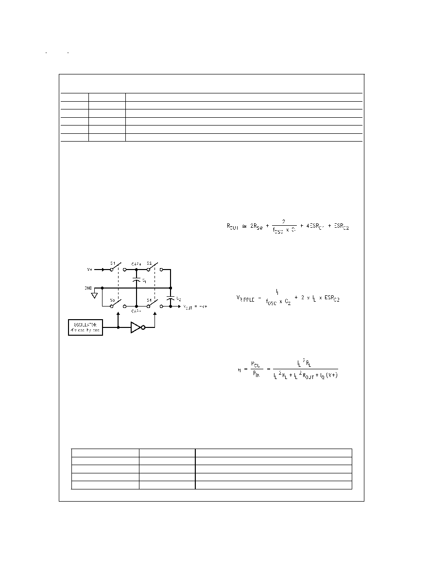
Circuit Description
The LM828 contains four large CMOS switches which are
switched in a sequence to invert the input supply voltage.
Energy transfer and storage are provided by external capaci-
tors.
Figure 2 illustrates the voltage conversion scheme.
When S
1
and S
3
are closed, C
1
charges to the supply volt-
age V+. During this time interval, switches S
2
and S
4
are
open. In the second time interval, S
1
and S
3
are open; at the
same time, S
2
and S
4
are closed, C
1
is charging C
2
. After a
number of cycles, the voltage across C
2
will be pumped to
V+. Since the anode of C
2
is connected to ground, the output
at the cathode of C
2
equals -(V+) when there is no load cur-
rent. The output voltage drop when a load is added is deter-
mined by the parasitic resistance (R
ds(on)
of the MOSFET
switches and the ESR of the capacitors) and the charge
transfer loss between capacitors.
Application Information
Simple Negative Voltage Converter
The main application of LM828 is to generate a negative
supply voltage. The voltage inverter circuit uses only two ex-
ternal capacitors as shown in the Basic Application Circuits.
The range of the input supply voltage is 1.8V to 5.5V.
The output characteristics of this circuit can be approximated
by an ideal voltage source in series with a resistance. The
voltage source equals -(V+). The output resistance, R
out
, is
a function of the ON resistance of the internal MOSFET
switches, the oscillator frequency, the capacitance and the
ESR of both C
1
and C
2
. Since the switching current charging
and discharging C
1
is approximately twice as the output cur-
rent, the effect of the ESR of the pumping capacitor C
1
will
be multiplied by four in the output resistance. The output ca-
pacitor C
2
is charging and discharging at a current approxi-
mately equal to the output current, therefore, this ESR term
only counts once in the output resistance. A good approxi-
mation of R
out
is:
where R
SW
is the sum of the ON resistance of the internal
MOSFET switches shown in
Figure 2.
High capacitance, low ESR capacitors will reduce the output
resistance.
The peak-to-peak output voltage ripple is determined by the
oscillator frequency, the capacitance and ESR of the output
capacitor C
2
:
Again, using a low ESR capacitor will result in lower ripple.
Capacitor Selection
The output resistance and ripple voltage are dependent on
the capacitance and ESR values of the external capacitors.
The output voltage drop is the load current times the output
resistance, and the power efficiency is
Where I
Q
(V+) is the quiescent power loss of the IC device,
and I
L
2
R
out
is the conversion loss associated with the switch
on-resistance, the two external capacitors and their ESRs.
The selection of capacitors is based on the specifications of
the dropout voltage (which equals I
out
R
out
), the output volt-
age ripple, and the converter efficiency. Low ESR capacitors
(following table) are recommended to maximize efficiency,
reduce the output voltage drop and voltage ripple.
Low ESR Capacitor Manufacturers
Manufacturer
Phone
Capacitor Type
Nichicon Corp.
(708)-843-7500
PL & PF series, through-hole aluminum electrolytic
AVX Corp.
(803)-448-9411
TPS series, surface-mount tantalum
Sprague
(207)-324-4140
593D, 594D, 595D series, surface-mount tantalum
Sanyo
(619)-661-6835
OS-CON series, through-hole aluminum electrolytic
DS100137-26
FIGURE 2. Voltage Inverting Principle
www.national.com
5