 | –≠–ª–µ–∫—Ç—Ä–æ–Ω–Ω—ã–π –∫–æ–º–ø–æ–Ω–µ–Ω—Ç: LMC555 | –°–∫–∞—á–∞—Ç—å:  PDF PDF  ZIP ZIP |

LMC555
CMOS Timer
General Description
The LMC555 is a CMOS version of the industry standard
555 series general purpose timers. In addition to the stan-
dard package (SOIC, MSOP, and MDIP) the LMC555 is also
available in a chip sized package (8 Bump micro SMD) using
National's micro SMD package technology. The LMC555 of-
fers the same capability of generating accurate time delays
and frequencies as the LM555 but with much lower power
dissipation and supply current spikes. When operated as a
one-shot, the time delay is precisely controlled by a single
external resistor and capacitor. In the stable mode the oscil-
lation frequency and duty cycle are accurately set by two ex-
ternal resistors and one capacitor. The use of National Semi-
conductor's LMCMOS
TM
process extends both the frequency
range and low supply capability.
Features
n
Less than 1 mW typical power dissipation at 5V supply
n
3 MHz astable frequency capability
n
1.5V supply operating voltage guaranteed
n
Output fully compatible with TTL and CMOS logic at 5V
supply
n
Tested to -10 mA, +50 mA output current levels
n
Reduced supply current spikes during output transitions
n
Extremely low reset, trigger, and threshold currents
n
Excellent temperature stability
n
Pin-for-pin compatible with 555 series of timers
n
Available in 8 pin MSOP Package and 8-Bump micro
SMD package
Block and Connection Diagrams
LMCMOS
TM
is a trademark of National Semiconductor Corp.
8-Pin SOIC, MSOP,
and MDIP Packages
DS008669-1
Top View
8-Bump micro SMD
DS008669-9
Top View
(bump side down)
February 2000
LMC555
CMOS
T
imer
© 2000 National Semiconductor Corporation
DS008669
www.national.com
Ordering Information
Package
Temperature Range
Package Marking
Transport Media
NSC
Drawing
Industrial
-40∞C to +85∞C
8-LeadSmall Outline
(SO)
LMC555CM
LMC555CM
Rails
M08A
LMC555CMX
LMC555CM
2.5k Units Tape and Reel
8-Lead Mini Small
Outline (MSOP)
LMC555CMM
ZC5
1k Units Tape and Reel
MUA08A
LMC555CMMX
ZC5
3.5k Units Tape and Reel
8-Lead Molded Dip
(MDIP)
LMC555CN
LMC555CN
Rails
N08E
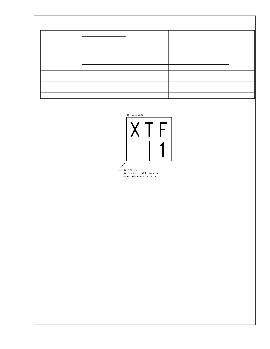
8-Bump micro SMD
LMC555CBP
F1
250 Units Tape and Reel
BPA08EFB
LMC555CBPX
F1
3k Units Tape and Reel
Metronome Circuit
LMC555CBPEVAL
N/A
N/A
N/A
micro SMD Marking Orientation
Top View
DS008669-23
Bumps are numbered counter-clockwise
LMC555
www.national.com
2
Absolute Maximum Ratings
(Notes 2, 3)
If Military/Aerospace specified devices are required,
please contact the National Semiconductor Sales Office/
Distributors for availability and specifications.
Supply Voltage, V
+
15V
Input Voltages, V
TRIG
, V
RES
, V
CTRL
,
V
THRESH
-0.3V to V
S
+ 0.3V
Output Voltages, V
O
, V
DIS
15V
Output Current I
O
, I
DIS
100 mA
Storage Temperature Range
-65∞C to +150∞C
Soldering Information
MDIP Soldering (10 seconds)
260∞C
SOIC, MSOP Vapor Phase (60
sec)
215∞C
SOIC, MSOP Infrared (15 sec)
220∞C
Note: See AN-450 "Surface Mounting Methods and Their Effect on Product
Reliability" for other methods of soldering surface mount devices.
Operating Ratings
(Notes 2, 3)
Termperature Range
-40∞C to +85∞C
Thermal Resistance (
JA
) (Note 2)
SO, 8-lead Small Outline
169∞C/W
MSOP, 8-lead Mini Small
Outline
225∞C/W
MDIP, 8-lead Molded Dip
111∞C/W
8-Bump micro SMD
220∞C/W
Maximum Allowable Power
Dissipation
@
25∞C
MDIP-8
1126mW
SO-8
740mW
MSOP-8
555mW
8 Bump micro SMD
568mW
Electrical Characteristics
(Notes 1, 2)
Test Circuit, T = 25∞C, all switches open, RESET to V
S
unless otherwise noted
Symbol
Parameter
Conditions
Min
Typ
Max
Units
(Limits)
I
S
Supply Current
V
S
= 1.5V
V
S
= 5V
V
S
= 12V
50
100
150
150
250
400
µA
V
CTRL
Control Voltage
V
S
= 1.5V
V
S
= 5V
V
S
= 12V
0.8
2.9
7.4
1.0
3.3
8.0
1.2
3.8
8.6
V
V
DIS
Discharge Saturation
Voltage
V
S
= 1.5V, I
DIS
= 1 mA
V
S
= 5V, I
DIS
= 10 mA
75
150
150
300
mV
V
OL
Output Voltage (Low)
V
S
= 1.5V, I
O
= 1 mA
V
S
= 5V, I
O
= 8 mA
V
S
= 12V, I
O
= 50 mA
0.2
0.3
1.0
0.4
0.6
2.0
V
V
OH
Output Voltage
(High)
V
S
= 1.5V, I
O
= -0.25 mA
V
S
= 5V, I
O
= -2 mA
V
S
= 12V, I
O
= -10 mA
1.0
4.4
10.5
1.25
4.7
11.3
V
V
TRIG
Trigger Voltage
V
S
= 1.5V
V
S
= 12V
0.4
3.7
0.5
4.0
0.6
4.3
V
I
TRIG
Trigger Current
V
S
= 5V
10
pA
V
RES
Reset Voltage
V
S
= 1.5V (Note 4)
V
S
= 12V
0.4
0.4
0.7
0.75
1.0
1.1
V
I
RES
Reset Current
V
S
= 5V
10
pA
I
THRESH
Threshold Current
V
S
= 5V
10
pA
I
DIS
Discharge Leakage
V
S
= 12V
1.0
100
nA
t
Timing Accuracy
SW 2, 4 Closed
V
S
= 1.5V
V
S
= 5V
V
S
= 12V
0.9
1.0
1.0
1.1
1.1
1.1
1.25
1.20
1.25
ms
t/
V
S
Timing Shift with Supply
V
S
= 5V
±
1V
0.3
%/V
t/
T
Timing Shift with
Temperature
V
S
= 5V
-40∞C
T
+85∞C
75
ppm/∞C
f
A
Astable Frequency
SW 1, 3 Closed, V
S
= 12V
4.0
4.8
5.6
kHz
f
MAX
Maximum Frequency
Max. Freq. Test Circuit, V
S
= 5V
3.0
MHz
t
R
, t
F
Output Rise and
Fall Times
Max. Freq. Test Circuit
V
S
= 5V, C
L
= 10 pF
15
ns
LMC555
www.national.com
3

Electrical Characteristics
(Notes 1, 2)
Test Circuit, T = 25∞C, all switches open, RESET to V
S
unless otherwise noted (Continued)
Symbol
Parameter
Conditions
Min
Typ
Max
Units
(Limits)
t
PD
Trigger Propagation Delay
V
S
= 5V, Measure Delay
from Trigger to Output
100
ns
Note 1: All voltages are measured with respect to the ground pin, unless otherwise specified.
Note 2: Absolute Maximum Ratings indicate limits beyond which damage to the device may occur. Operating Ratings indicate conditions for which the device is func-
tional, but do not guarantee specific performance limits. Electrical Characteristics state DC and AC electrical specifications under particular test conditions which guar-
antee specific performance limits. This assumes that the device is within the Operating Ratings. Specifications are not guaranteed for parameters where no limit is
given, however, the typical value is a good indication of device performance.
Note 3: See AN-450 for other methods of soldering surface mount devices, and also AN-1112 for micro SMD considerations.
Note 4: If the RESET pin is to be used at temperatures of -20∞C and below V
S
is required to be 2.0V or greater.
Note 5: For device pinout please refer to table 1
TABLE 1. Package Pinout Names vs. Pin Function
Pin Function
Package Pin numbers
8-Pin SO,MSOP, and MDIP
8-Bump micro SMD
GND
1
7
Trigger
2
6
Output
3
5
Reset
4
4
Control Voltage
5
3
Threshold
6
2
Discharge
7
1
V
+
8
8
Test Circuit (Note 5)
DS008669-2
Maximum Frequency Test Circuit (Note 5)
DS008669-3
LMC555
www.national.com
4
Application Info
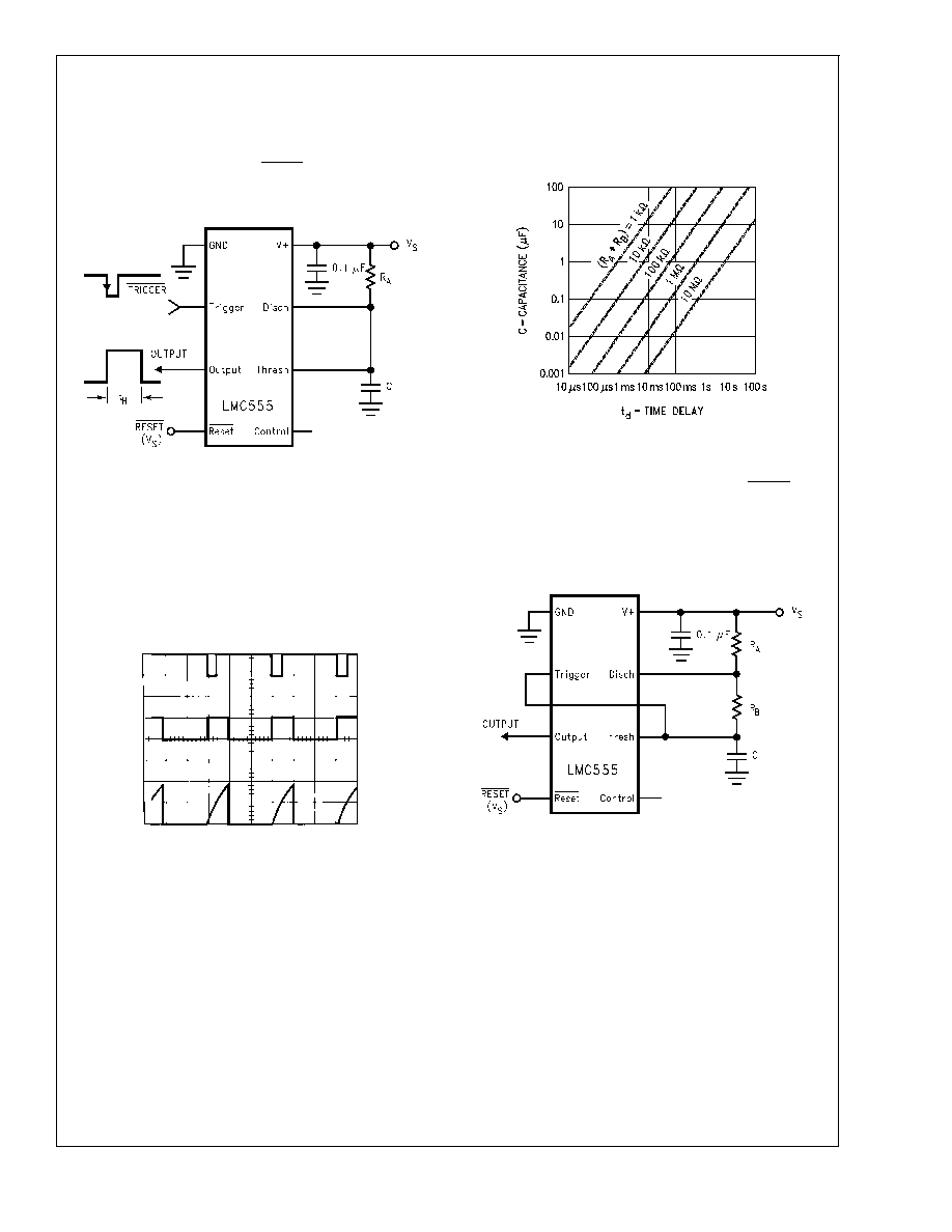
MONOSTABLE OPERATION
In this mode of operation, the timer functions as a one-shot
(
Figure 1). The external capacitor is initially held discharged
by internal circuitry. Upon application of a negative trigger
pulse of less than 1/3 V
S
to the Trigger terminal, the flip-flop
is set which both releases the short circuit across the capaci-
tor and drives the output high.
The voltage across the capacitor then increases exponen-
tially for a period of t
H
= 1.1 R
A
C, which is also the time that
the output stays high, at the end of which time the voltage
equals 2/3 V
S
. The comparator then resets the flip-flop which
in turn discharges the capacitor and drives the output to its
low state.
Figure 2 shows the waveforms generated in this
mode of operation. Since the charge and the threshold level
of the comparator are both directly proportional to supply
voltage, the timing internal is independent of supply.
Reset overrides Trigger, which can override threshold.
Therefore the trigger pulse must be shorter than the desired
t
H
. The minimum pulse width for the Trigger is 20ns, and it is
400ns for the Reset. During the timing cycle when the output
is high, the further application of a trigger pulse will not effect
the circuit so long as the trigger input is returned high at least
10µs before the end of the timing interval. However the cir-
cuit can be reset during this time by the application of a
negative pulse to the reset terminal. The output will then re-
main in the low state until a trigger pulse is again applied.
When the reset function is not use, it is recommended that it
be connected to V
+
to avoid any possibility of false triggering.
Figure 3 is a nomograph for easy determination of RC values
for various time delays.
Note: In monstable operation, the trigger should be driven high before the
end of timing cycle.
ASTABLE OPERATION
If the circuit is connected as shown in
Figure 4 (Trigger and
Threshold terminals connected together) it will trigger itself
and free run as a multivibrator. The external capacitor
charges through R
A
+ R
B
and discharges through R
B
. Thus
the duty cycle may be precisely set by the ratio of these two
resistors.
In this mode of operation, the capacitor charges and dis-
charges between 1/3 V
S
and 2/3 V
S
. As in the triggered
mode, the charge and discharge times, and therefore the fre-
quency are independent of the supply voltage.
Figure 5 shows the waveform generated in this mode of
operation.
DS008669-4
FIGURE 1. Monostable (One-Shot)
DS008669-10
V
CC
= 5V
Top Trace: Input 5V/Div.
TIME = 0.1 ms/Div.
Middle Trace: Output 5V/Div.
R
A
= 9.1k
Bottom Trace: Capacitor Voltage 2V/Div.
C = 0.01µF
FIGURE 2. Monostable Waveforms
DS008669-11
FIGURE 3. Time Delay
DS008669-5
FIGURE 4. Astable (Variable Duty Cycle Oscillator)
LMC555
www.national.com
5