 | –≠–ª–µ–∫—Ç—Ä–æ–Ω–Ω—ã–π –∫–æ–º–ø–æ–Ω–µ–Ω—Ç: LMC6034 | –°–∫–∞—á–∞—Ç—å:  PDF PDF  ZIP ZIP |

LMC6034
CMOS Quad Operational Amplifier
General Description
The LMC6034 is a CMOS quad operational amplifier which
can operate from either a single supply or dual supplies. Its
performance features include an input common-mode range
that reaches ground, low input bias current, and high voltage
gain into realistic loads, such as 2 k
and 600
.
This chip is built with National's advanced Double-Poly
Silicon-Gate CMOS process.
See the LMC6032 datasheet for a CMOS dual operational
amplifier with these same features. For higher performance
characteristics refer to the LMC660.
Features
n
Specified for 2 k
and 600
loads
n
High voltage gain:
126 dB
n
Low offset voltage drift:
2.3 µV/∞C
n
Ultra low input bias current:
40 fA
n
Input common-mode range includes V
-
n
Operating Range from +5V to +15V supply
n
I
SS
= 400 µA/amplifier; independent of V
+
n
Low distortion:
0.01% at 10 kHz
n
Slew rate:
1.1 V/µs
n
Improved performance over TLC274
Applications
n
High-impedance buffer or preamplifier
n
Current-to-voltage converter
n
Long-term integrator
n
Sample-and-hold circuit
n
Medical instrumentation
Connection Diagram
Ordering Information
Temperature Range
Package
NSC
Drawing
Transport
Media
Industrial
-40∞C
T
J
+85∞C
LMC6034IN
14-Pin
N14A
Rail
Molded DIP
LMC6034IM
14-Pin
M14A
Rail
Small Outline
Tape and Reel
14-Pin DIP/SO
DS011134-1
Top View
May 1998
LMC6034
CMOS
Quad
Operational
Amplifier
© 1999 National Semiconductor Corporation
DS011134
www.national.com

Absolute Maximum Ratings
(Note 1)
If Military/Aerospace specified devices are required,
please contact the National Semiconductor Sales Office/
Distributors for availability and specifications.
Differential Input Voltage
±
Supply Voltage
Supply Voltage (V
+
- V
-
)
16V
Output Short Circuit to V
+
(Note 10)
Output Short Circuit to V
-
(Note 2)
Lead Temperature
(Soldering, 10 sec.)
260∞C
Storage Temperature Range
-65∞C to +150∞C
Power Dissipation
(Note 3)
Voltage at Output/Input Pin
(V
+
) +0.3V, (V
-
) -0.3V
Current at Output Pin
±
18 mA
Current at Input Pin
±
5 mA
Current at Power Supply Pin
35 mA
Junction Temperature (Note 3)
150∞C
ESD Tolerance (Note 4)
1000V
Operating Ratings
(Note 1)
Temperature Range
-40∞C
T
J
+85∞C
Supply Voltage Range
4.75V to 15.5V
Power Dissipation
(Note 11)
Thermal Resistance (
JA
), (Note 12)
14-Pin DIP
85∞C/W
14-Pin SO
115∞C/W
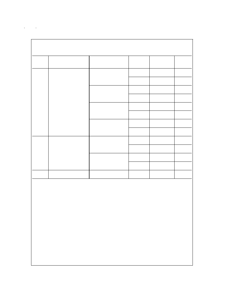
DC Electrical Characteristics
Unless otherwise specified, all limits guaranteed for T
J
= 25∞C. Boldface limits apply at the temperature extremes. V
+
= 5V,
V
-
= GND = 0V, V
CM
= 1.5V, V
OUT
= 2.5V, and R
L
>
1M unless otherwise specified.
Symbol
Parameter
Conditions
Typical
(Note 5)
LMC6034I
Units
Limit
(Note 6)
V
OS
Input Offset Voltage
1
9
mV
11
max
V
OS
/
T
Input Offset Voltage
2.3
µV/∞C
Average Drift
I
B
Input Bias Current
0.04
pA
200
max
I
OS
Input Offset Current
0.01
pA
100
max
R
IN
Input Resistance
>
1
Tera
CMRR
Common Mode
0V
V
CM
12V
83
63
dB
Rejection Ratio
V
+
= 15V
60
min
+PSRR
Positive Power Supply
5V
V
+
15V
83
63
dB
Rejection Ratio
V
O
= 2.5V
60
min
-PSRR
Negative Power Supply
0V
V
-
-10V
94
74
dB
Rejection Ratio
70
min
V
CM
Input Common-Mode
V
+
= 5V & 15V
-0.4
-0.1
V
Voltage Range
For CMRR
50 dB
0
max
V
+
- 1.9
V
+
- 2.3
V
V
+
- 2.6
min
A
V
Large Signal Voltage Gain
R
L
= 2 k
(Note 7)
2000
200
V/mV
Sourcing
100
min
Sinking
500
90
V/mV
40
min
R
L
= 600
(Note 7)
1000
100
V/mV
Sourcing
75
min
Sinking
250
50
V/mV
20
min
www.national.com
2
DC Electrical Characteristics
(Continued)
Unless otherwise specified, all limits guaranteed for T
J
= 25∞C. Boldface limits apply at the temperature extremes. V
+
= 5V,
V
-
= GND = 0V, V
CM
= 1.5V, V
OUT
= 2.5V, and R
L
>
1M unless otherwise specified.
Symbol
Parameter
Conditions
Typical
(Note 5)
LMC6034I
Units
Limit
(Note 6)
V
O
Output Voltage Swing
V
+
= 5V
4.87
4.20
V
R
L
= 2 k
to 2.5V
4.00
min
0.10
0.25
V
0.35
max
V
+
= 5V
4.61
4.00
V
R
L
= 600
to 2.5V
3.80
min
0.30
0.63
V
0.75
max
V
+
= 15V
14.63
13.50
V
R
L
= 2 k
to 7.5V
13.00
min
0.26
0.45
V
0.55
max
V
+
= 15V
13.90
12.50
V
R
L
= 600
to 7.5V
12.00
min
0.79
1.45
V
1.75
max
I
O
Output Current
V
+
= 5V
22
13
mA
Sourcing, V
O
= 0V
9
min
Sinking, V
O
= 5V
21
13
mA
9
min
V
+
= 15V
40
23
mA
Sourcing, V
O
= 0V
15
min
Sinking, V
O
= 13V
39
23
mA
(Note 10)
15
min
I
S
Supply Current
All Four Amplifiers
1.5
2.7
mA
V
O
= 1.5V
3.0
max
www.national.com
3

AC Electrical Characteristics
Unless otherwise specified, all limits guaranteed for T
J
= 25∞C. Boldface limits apply at the temperature extremes. V
+
= 5V,
V
-
= GND = 0V, V
CM
= 1.5V, V
OUT
= 2.5V, and R
L
>
1M unless otherwise specified.
Symbol
Parameter
Conditions
Typical
(Note 5)
LMC6034I
Units
Limit
(Note 6)
SR
Slew Rate
(Note 8)
1.1
0.8
V/µs
0.4
min
GBW
Gain-Bandwidth Product
1.4
MHz
M
Phase Margin
50
Deg
G
M
Gain Margin
17
dB
Amp-to-Amp Isolation
(Note 9)
130
dB
e
n
Input-Referred Voltage Noise
F = 1 kHz
22
i
n
Input-Referred Current Noise
F = 1 kHz
0.0002
THD
Total Harmonic Distortion
F = 10 kHz, A
V
= -10
R
L
= 2 k
, V
O
= 8 V
PP
0.01
%
±
5V Supply
Note 1: Absolute Maximum Ratings indicate limits beyond which damage to the component may occur. Operating Ratings indicate conditions for which the device
is intended to be functional, but do not guarantee specific performance limits. For guaranteed specifications and test conditions, see the Electrical Characteristics.
The guaranteed specifications apply only for the test conditions listed.
Note 2: Applies to both single-supply and split-supply operation. Continuous short circuit operation at elevated ambient temperature and/or multiple Op Amp shorts
can result in exceeding the maximum allowed junction temperature of 150∞C. Output currents in excess of
±
30 mA over long term may adversely affect reliability.
Note 3: The maximum power dissipation is a function of T
J(max)
,
JA
, T
A
. The maximum allowable power dissipation at any ambient temperature is P
D
=
(T
J(max)
≠T
A
)/
JA
.
Note 4: Human body model, 100 pF discharged through a 1.5 k
resistor.
Note 5: Typical values represent the most likely parametric norm.
Note 6: All limits are guaranteed at room temperature (standard type face) or at operating temperature extremes (bold type face).
Note 7: V
+
= 15V, V
CM
= 7.5V, and R
L
connected to 7.5V. For Sourcing tests, 7.5V
V
O
11.5V. For Sinking tests, 2.5V
V
O
7.5V.
Note 8: V
+
= 15V. Connected as Voltage Follower with 10V step input. Number specified is the slower of the positive and negative slew rates.
Note 9: Input referred. V
+
= 15V and R
L
= 10 k
connected to V
+
/2. Each amp excited in turn with 1 kHz to produce V
O
= 13 V
PP
.
Note 10: Do not connect output to V
+
, when V
+
is greater than 13V or reliability may be adversely affected.
Note 11: For operating at elevated temperatures the device must be derated based on the thermal resistance
JA
with P
D
= (T
J
- T
A
)/
JA
.
Note 12: All numbers apply for packages soldered directly into a PC board.
Typical Performance Characteristics
V
S
=
±
7.5V, T
A
= 25∞C unless otherwise specified
Supply Current
vs Supply Voltage
DS011134-23
Input Bias Current
DS011134-24
Output Characteristics
Current Sinking
DS011134-25
www.national.com
4

Typical Performance Characteristics
V
S
=
±
7.5V, T
A
= 25∞C unless otherwise specified (Continued)
Applications Hint
Amplifier Topolgy
The topology chosen for the LMC6034, shown in
Figure 1, is
unconventional (compared to general-purpose op amps) in
that the traditional unity-gain buffer output stage is not used;
instead, the output is taken directly from the output of the in-
tegrator, to allow a larger output swing. Since the buffer tra-
ditionally delivers the power to the load, while maintaining
high op amp gain and stability, and must withstand shorts to
either rail, these tasks now fall to the integrator.
As a result of these demands, the integrator is a compound
affair with an embedded gain stage that is doubly fed forward
(via C
f
and Cff) by a dedicated unity-gain compensation
driver. In addition, the output portion of the integrator is a
push-pull configuration for delivering heavy loads. While
sinking current the whole amplifier path consists of three
gain stages with one stage fed forward, whereas while
sourcing the path contains four gain stages with two fed
forward.
Output Characteristics
Current Sourcing
DS011134-27
Input Voltage Noise
vs Frequency
DS011134-28
CMRR vs Frequency
DS011134-29
Open-Loop Frequency
Response
DS011134-30
Frequency Response
vs Capacitive Load
DS011134-31
Non-Inverting Large Signal
Pulse Response
DS011134-32
Stability vs
Capacitive Load
DS011134-33
Stability vs
Capacitive Load
DS011134-34
Note: Avoid resistive loads of less than 500
, as they may cause instability.
www.national.com
5