LMC6035/LMC6036
Low Power 2.7V Single Supply CMOS Operational
Amplifiers
General Description
The LMC6035/6 is an economical, low voltage op amp ca-
pable of rail-to-rail output swing into loads of 600
.
LMC6035 is available in a chip sized package (8-Bump mi-
cro SMD) using National's micro SMD package technology.
Both allow for single supply operation and are guaranteed
for 2.7V, 3V, 5V and 15V supply voltage. The 2.7 supply volt-
age corresponds to the End-of-Life voltage (0.9V/cell) for
three NiCd or NiMH batteries in series, making the
LMC6035/6 well suited for portable and rechargeable sys-
tems. It also features a well behaved decrease in its specifi-
cations at supply voltages below its guaranteed 2.7V opera-
tion. This provides a "comfort zone" for adequate operation
at voltages significantly below 2.7V. Its ultra low input cur-
rents (I
IN
) makes it well suited for low power active filter ap-
plication, because it allows the use of higher resistor values
and lower capacitor values. In addition, the drive capability of
the LMC6035/6 gives these op amps a broad range of appli-
cations for low voltage systems.
Features
(Typical Unless Otherwise Noted)
n
LMC6035 in micro SMD Package
n
Guaranteed 2.7V, 3V, 5V and 15V Performance
n
Specified for 2 k
and 600
Loads
n
Wide Operating Range:
2.0V to 15.5V
n
Ultra Low Input Current:
20 fA
n
Rail-to-Rail Output Swing
@
600
:
200 mV from either rail at 2.7V
@
100 k
:
5 mV from either rail at 2.7V
n
High Voltage Gain:
126dB
n
Wide Input Common-Mode Voltage Range
-0.1V to 2.3V at Vs = 2.7V
n
Low Distortion:
0.01% at 10 kHz
Applications
n
Filters
n
High Impedance Buffer or Preamplifier
n
Battery Powered Electronics
n
Medical Instrumentation
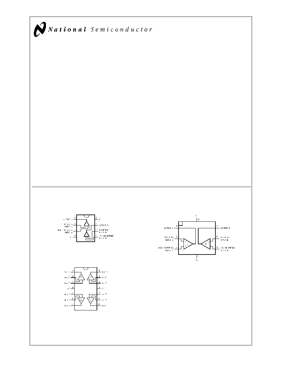
Connection Diagrams
8-Pin SO/MSOP
DS012830-1
Top View
14-Pin SO/TSSOP
DS012830-2
Top View
8-Bump micro SMD
DS012830-65
Top View
(Bump Side Down)
January 2000
LMC6035/LMC6036
Low
Power
2.7V
Single
Supply
CMOS
Operational
Amplifiers
� 2000 National Semiconductor Corporation
DS012830
www.national.com
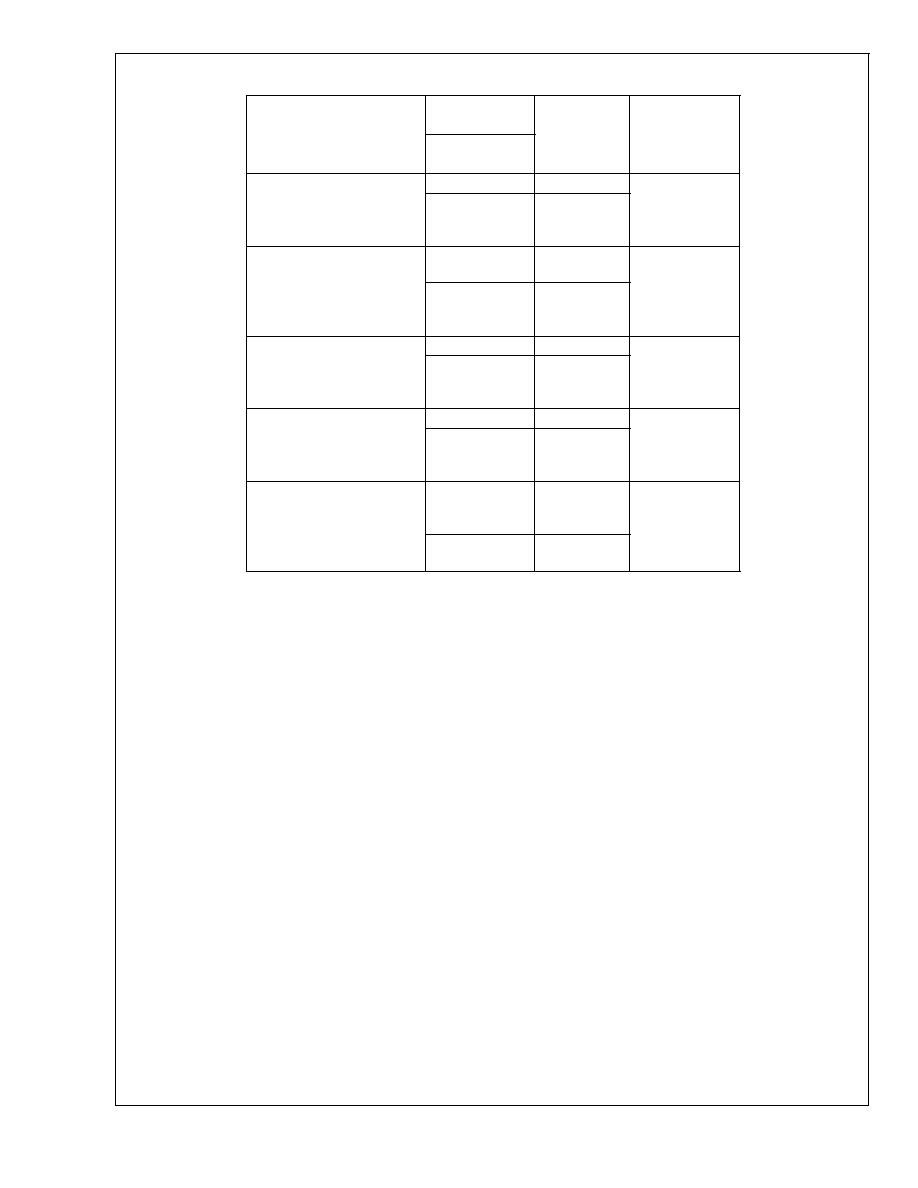
Ordering Information
Package
Temperature
Range
Transport
Media
NSC
Drawing
Industrial
-40�C to +85�C
8-pin Small Outline (SO)
LMC6035IM
Rails
M08A
LMC6035IMX
2.5k Units
Tape and
Reel
8-pin Mini Small Outline
(MSOP)
LMC6035IMM
1k Units Tape
and Reel
MUA08A
LMC6035IMMX
3.5k Units
Tape and
Reel
14-pin Small Outline (SO)
LMC6036IM
Rails
M14A
LMC6036IMX
2.5k Units
Tape and
Reel
14-pin Thin Shrink Small
Outline (TSSOP)
LMC6036IMT
Rails
MTC14
LMC6036IMTX
2.5k Units
Tape and
Reel
8-Bump micro SMD
LMC6035IBP
250 Units
Tape and
Reel
BPA08FFB
LMC6035IBPX
3k Units Tape
and Reel
LMC6035/LMC6036
www.national.com
2

Absolute Maximum Ratings
(Note 1)
If Military/Aerospace specified devices are required,
please contact the National Semiconductor Sales Office/
Distributors for availability and specifications.
ESD Tolerance (Note 2)
Human Body Model
3000V
Machine Model
300V
Differential Input Voltage
�
Supply Voltage
Supply Voltage (V
+
- V
-
)
16V
Output Short Circuit to V
+
(Note 8)
Output Short Circuit to V
-
(Note 3)
Lead Temperature (soldering, 10 sec.)
260�C
Current at Output Pin
�
18 mA
Current at Input Pin
�
5 mA
Current at Power Supply Pin
35 mA
Storage Temperature Range
-65�C to +150�C
Junction Temperature (Note 4)
150�C
Operating Ratings
(Note 1)
Supply Voltage
2.0V to 15.5V
Temperature Range
LMC6035I and LMC6036I
-40�C
T
J
+85�C
Thermal Resistance (
JA
)
MSOP, 8-pin Mini Surface Mount
230�C/W
M Package, 8-pin Surface Mount
175�C/W
M Package, 14-pin Surface Mount
127�C/W
MTC Package, 14-pin TSSOP
137�C/W
BP, 8-Bump micro SMD Package
220�C/W
DC Electrical Characteristics
Unless otherwise specified, all limits guaranteed for T
J
= 25�C, V
+
= 2.7V, V
-
= 0V, V
CM
= 1.0V, V
O
= 1.35V and R
L
>
1 M
.
Boldface limits apply at the temperature extremes.
Symbol
Parameter
Conditions
Typ
(Note 5)
LMC6035I
Units
LMC6036I
Limit (Note 6)
V
OS
Input Offset Voltage
0.5
5
mV
6
max
TCV
OS
Input Offset Voltage
2.3
�V/�C
Average Drift
I
IN
Input Current
(Note 11)
0.02
pA
90
max
I
OS
Input Offset Current
(Note 11)
0.01
pA
45
max
R
IN
Input Resistance
>
10
Tera
CMRR
Common Mode
0.7V
V
CM
12.7V
96
63
dB
Rejection Ratio
V
+
= 15V
60
min
+PSRR
Positive Power Supply
5V
V
+
15V,
93
63
dB
Rejection Ratio
V
O
= 2.5V
60
min
-PSRR
Negative Power Supply
0V
V
-
-10V
97
74
dB
Rejection Ratio
V
O
= 2.5V, V
+
= 5V
70
min
V
CM
Input Common-Mode
V
+
= 2.7V
-0.1
0.3
V
Voltage Range
For CMRR
40 dB
0.5
max
2.3
2.0
V
1.7
min
V
+
= 3V
-0.3
0.1
V
For CMRR
40 dB
0.3
max
2.6
2.3
V
2.0
min
V
+
= 5V
-0.5
-0.2
V
For CMRR
50 dB
0.0
max
4.5
4.2
V
3.9
min
V
+
= 15V
-0.5
-0.2
V
For CMRR
50 dB
0.0
max
14.4
14.0
V
13.7
min
LMC6035/LMC6036
www.national.com
3

DC Electrical Characteristics
(Continued)
Unless otherwise specified, all limits guaranteed for T
J
= 25�C, V
+
= 2.7V, V
-
= 0V, V
CM
= 1.0V, V
O
= 1.35V and R
L
>
1 M
.
Boldface limits apply at the temperature extremes.
Symbol
Parameter
Conditions
Typ
(Note 5)
LMC6035I
Units
LMC6036I
Limit (Note 6)
A
V
Large Signal Voltage Gain
R
L
= 600
Sourcing
1000
100
V/mV
(Note 7)
75
min
Sinking
250
25
V/mV
20
min
R
L
=2 k
Sourcing
2000
V/mV
Sinking
500
V/mV
V
O
Output Swing
V
+
= 2.7V
2.5
2.0
V
R
L
= 600
to 1.35V
1.8
min
0.2
0.5
V
0.7
max
V
+
= 2.7V
2.62
2.4
V
R
L
= 2 k
to 1.35V
2.2
min
0.07
0.2
V
0.4
max
V
+
= 15V
14.5
13.5
V
R
L
= 600
to 7.5V
13.0
min
0.36
1.25
V
1.50
max
V
+
= 15V
14.8
14.2
V
R
L
= 2 k
to 7.5V
13.5
min
0.12
0.4
V
0.5
max
I
O
Output Current
V
O
= 0V
Sourcing
8
4
mA
3
min
V
O
= 2.7V
Sinking
5
3
mA
2
min
I
S
Supply Current
LMC6035 for Both Amplifiers
0.65
1.6
mA
V
O
= 1.35V
1.9
max
LMC6036 for All Four Amplifiers
1.3
2.7
mA
V
O
= 1.35V
3.0
max
LMC6035/LMC6036
www.national.com
4

AC Electrical Characteristics
Unless otherwise specified, all limits guaranteed for T
J
= 25�C, V
+
= 2.7V, V
-
= 0V, V
CM
= 1.0V, V
O
= 1.35V and R
L
>
1 M
. Boldface limits apply at the temperature extremes.
Symbol
Parameter
Conditions
Typ
Units
(Note 5)
SR
Slew Rate
(Note 9)
1.5
V/�s
GBW
Gain Bandwidth Product
V
+
= 15V
1.4
MHz
m
Phase Margin
48
�
G
m
Gain Margin
17
dB
Amp-to-Amp Isolation
(Note 10)
130
dB
e
n
Input-Referred Voltage Noise
f = 1 kHz
27
V
CM
= 1V
i
n
Input Referred Current Noise
f = 1 kHz
0.2
THD
Total Harmonic Distortion
f = 10 kHz, A
V
= -10
R
L
= 2 k
, V
O
= 8 V
PP
0.01
%
V
+
= 10V
Note 1: Absolute Maximum Ratings indicate limits beyond which damage to the device may occur. Operating Ratings indicate conditions for which the device is in-
tended to be functional, but specific performance is not guaranteed. For guaranteed specifications and the test conditions, see the Electrical Characteristics.
Note 2: Human body model, 1.5 k
in series with 100 pF.
Note 3: Applies to both single-supply and split-supply operation. Continuous short circuit operation at elevated ambient temperature can result in exceeding the
maximum allowed junction temperature of 150�C. Output currents in excess of 30 mA over long term may adversely affect reliabilty.
Note 4: The maximum power dissipation is a function of T
J(max)
,
JA
, and T
A
. The maximum allowable power dissipation at any ambient temperature is P
D
= (T
J(max)
-T
A
)/
JA
. All numbers apply for packages soldered directly onto a PC board with no air flow.
Note 5: Typical Values represent the most likely parametric norm or one sigma value.
Note 6: All limits are guaranteed by testing or statistical analysis.
Note 7: V
+
= 15V, V
CM
= 7.5V and R
L
connected to 7.5V. For Sourcing tests, 7.5V
V
O
11.5V. For Sinking tests, 3.5V
V
O
7.5V.
Note 8: Do not short circuit output to V
+
when V
+
is greater than 13V or reliability will be adversely affected.
Note 9: V
+
= 15V. Connected as voltage follower with 10V step input. Number specified is the slower of the positive and negative slew rates.
Note 10: Input referred, V
+
= 15V and R
L
= 100 k
connected to 7.5V. Each amp excited in turn with 1 kHz to produce V
O
= 12 V
PP
.
Note 11: Guaranteed by design.
LMC6035/LMC6036
www.national.com
5