LMC6482
CMOS Dual Rail-To-Rail Input and Output Operational
Amplifier
General Description
The LMC6482 provides a common-mode range that extends
to both supply rails. This rail-to-rail performance combined
with excellent accuracy, due to a high CMRR, makes it
unique among rail-to-rail input amplifiers.
It is ideal for systems, such as data acquisition, that require
a large input signal range. The LMC6482 is also an excellent
upgrade for circuits using limited common-mode range am-
plifiers such as the TLC272 and TLC277.
Maximum dynamic signal range is assured in low voltage
and single supply systems by the LMC6482's rail-to-rail out-
put swing. The LMC6482's rail-to-rail output swing is guaran-
teed for loads down to 600
.
Guaranteed low voltage characteristics and low power dissi-
pation make the LMC6482 especially well-suited for
battery-operated systems.
LMC6482 is also available in MSOP package which is al-
most half the size of a SO-8 device.
See the LMC6484 data sheet for a Quad CMOS operational
amplifier with these same features.
Features
(Typical unless otherwise noted)
n
Rail-to-Rail Input Common-Mode Voltage Range
(Guaranteed Over Temperature)
n
Rail-to-Rail Output Swing (within 20 mV of supply rail,
100 k
load)
n
Guaranteed 3V, 5V and 15V Performance
n
Excellent CMRR and PSRR:
82 dB
n
Ultra Low Input Current:
20 fA
n
High Voltage Gain (R
L
= 500 k
):
130 dB
n
Specified for 2 k
and 600
loads
n
Available in MSOP Package
Applications
n
Data Acquisition Systems
n
Transducer Amplifiers
n
Hand-held Analytic Instruments
n
Medical Instrumentation
n
Active Filter, Peak Detector, Sample and Hold, pH
Meter, Current Source
n
Improved Replacement for TLC272, TLC277
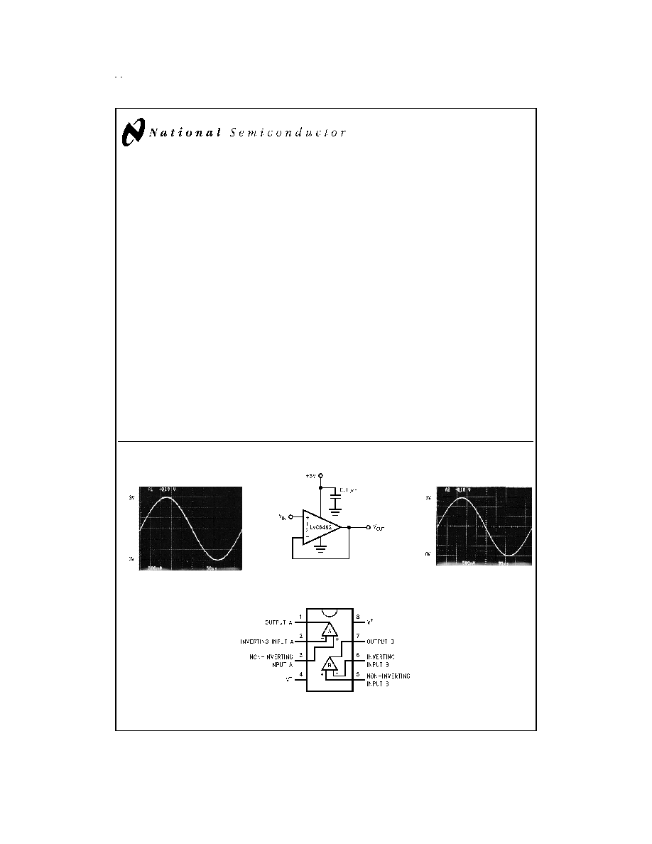
3V Single Supply Buffer Circuit
Connection Diagram
Rail-To-Rail Input
DS011713-1
DS011713-2
Rail-To-Rail Output
DS011713-3
DS011713-4
November 1997
LMC6482
CMOS
Dual
Rail-T
o-Rail
Input
and
Output
Operational
Amplifier
© 1999 National Semiconductor Corporation
DS011713
www.national.com

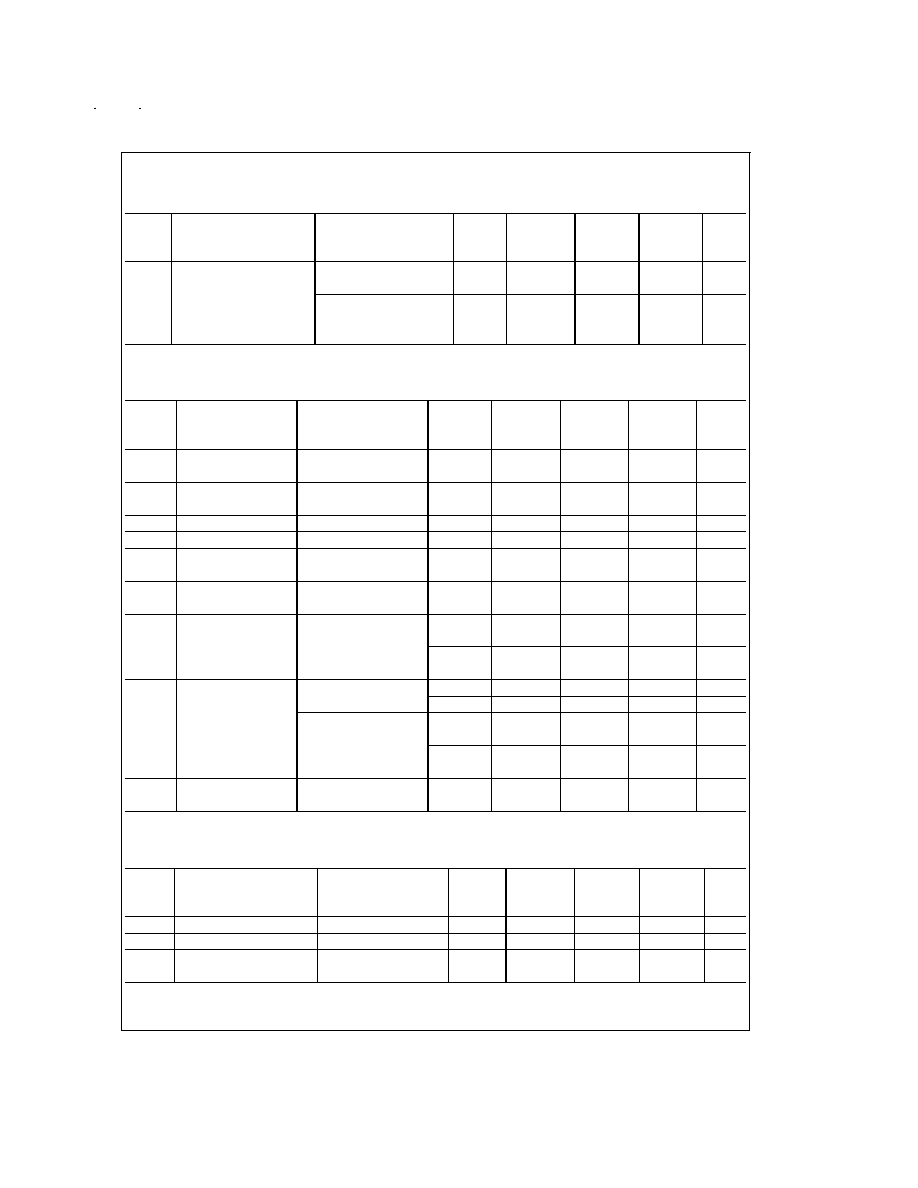
Ordering Information
Package
Temperature Range
NSC
Drawing
Transport
Media
Package Marking
Military
Industrial
-55∞C to +125∞C
-40∞C to +85∞C
8-Pin
LMC6482MN
LMC6482AIN,
N08E
Rail
LMC6482MN,
Molded DIP
LMC6482IN
LMC6482AIN, LMC6482IN
8-pin
LMC6482AIM,
M08A
Rail
LMC6482AIM, LMC6482IM
Small Outline
LMC6482IM
Tape and Reel
8-pin
LMC6482AMJ/883
J08A
Rail
LMC6482AMJ/883Q5962-9453401MPA
Ceramic DIP
8-pin
LMC6482IMM
MUA08A
Rail
A10
Mini SO
Tape and Reel
www.national.com
2

Absolute Maximum Ratings
(Note 1)
If Military/Aerospace specified devices are required,
please contact the National Semiconductor Sales Office/
Distributors for availability and specifications.
ESD Tolerance (Note 2)
1.5 kV
Differential Input Voltage
±
Supply Voltage
Voltage at Input/Output Pin
(V
+
) +0.3V, (V
-
) -0.3V
Supply Voltage (V
+
- V
-
)
16V
Current at Input Pin (Note 12)
±
5 mA
Current at Output Pin
(Notes 3, 8)
±
30 mA
Current at Power Supply Pin
40 mA
Lead Temperature
(Soldering, 10 sec.)
260∞C
Storage Temperature Range
-65∞C to +150∞C
Junction Temperature (Note 4)
150∞C
Operating Ratings
(Note 1)
Supply Voltage
3.0V
V+
15.5V
Junction Temperature Range
LMC6482AM
-55∞C
T
J
+125∞C
LMC6482AI, LMC6482I
-40∞C
T
J
+85∞C
Thermal Resistance (
JA
)
N Package, 8-Pin Molded DIP
90∞C/W
M Package, 8-Pin Surface Mount
155∞C/W
MSOP package, 8-Pin Mini SO
194∞C/W
DC Electrical Characteristics
Unless otherwise specified, all limits guaranteed for T
J
= 25∞C, V
+
= 5V, V
-
= 0V, V
CM
= V
O
= V
+
/2 and R
L
>
1M. Boldface
limits apply at the temperature extremes.
Symbol
Parameter
Conditions
Typ
(Note 5)
LMC6482AI
LMC6482I
LMC6482M
Units
Limit
Limit
Limit
(Note 6)
(Note 6)
(Note 6)
V
OS
Input Offset Voltage
0.11
0.750
3.0
3.0
mV
1.35
3.7
3.8
max
TCV
OS
Input Offset Voltage
1.0
µV/∞C
Average Drift
I
B
Input Current
(Note 13)
0.02
4.0
4.0
10.0
pA
max
I
OS
Input Offset Current
(Note 13)
0.01
2.0
2.0
5.0
pA
max
C
IN
Common-Mode
3
pF
Input Capacitance
R
IN
Input Resistance
>
10
Tera
CMRR
Common Mode
0V
V
CM
15.0V
82
70
65
65
dB
min
Rejection Ratio
V
+
= 15V
67
62
60
0V
V
CM
5.0V
82
70
65
65
V
+
= 5V
67
62
60
+PSRR
Positive Power Supply
5V
V
+
15V, V
-
= 0V
82
70
65
65
dB
Rejection Ratio
V
O
= 2.5V
67
62
60
min
-PSRR
Negative Power Supply
-5V
V
-
-15V, V
+
= 0V
82
70
65
65
dB
Rejection Ratio
V
O
= -2.5V
67
62
60
min
V
CM
Input Common-Mode
V
+
= 5V and 15V
V
-
- 0.3
- 0.25
- 0.25
- 0.25
V
Voltage Range
For CMRR
50 dB
0
0
0
max
V
+
+ 0.3V
V
+
+ 0.25
V
+
+ 0.25
V
+
+ 0.25
V
V
+
V
+
V
+
min
A
V
Large Signal
R
L
= 2 k
Sourcing
666
140
120
120
V/mV
Voltage Gain
(Notes 7, 13)
84
72
60
min
Sinking
75
35
35
35
V/mV
20
20
18
min
R
L
= 600
Sourcing
300
80
50
50
V/mV
(Notes 7, 13)
48
30
25
min
Sinking
35
20
15
15
V/mV
13
10
8
min
www.national.com
3

DC Electrical Characteristics
(Continued)
Unless otherwise specified, all limits guaranteed for T
J
= 25∞C, V
+
= 5V, V
-
= 0V, V
CM
= V
O
= V
+
/2 and R
L
>
1M. Boldface
limits apply at the temperature extremes.
Symbol
Parameter
Conditions
Typ
(Note 5)
LMC6482AI
LMC6482I
LMC6482M
Units
Limit
Limit
Limit
(Note 6)
(Note 6)
(Note 6)
V
O
Output Swing
V
+
= 5V
4.9
4.8
4.8
4.8
V
R
L
= 2 k
to V
+
/2
4.7
4.7
4.7
min
0.1
0.18
0.18
0.18
V
0.24
0.24
0.24
max
V
+
= 5V
4.7
4.5
4.5
4.5
V
R
L
= 600
to V
+
/2
4.24
4.24
4.24
min
0.3
0.5
0.5
0.5
V
0.65
0.65
0.65
max
V
+
= 15V
14.7
14.4
14.4
14.4
V
R
L
= 2 k
to V
+
/2
14.2
14.2
14.2
min
0.16
0.32
0.32
0.32
V
0.45
0.45
0.45
max
V
+
= 15V
14.1
13.4
13.4
13.4
V
R
L
= 600
to V
+
/2
13.0
13.0
13.0
min
0.5
1.0
1.0
1.0
V
1.3
1.3
1.3
max
I
SC
Output Short Circuit
Sourcing, V
O
= 0V
20
16
16
16
mA
Current
12
12
10
min
V
+
= 5V
Sinking, V
O
= 5V
15
11
11
11
mA
9.5
9.5
8.0
min
I
SC
Output Short Circuit
Sourcing, V
O
= 0V
30
28
28
28
mA
Current
22
22
20
min
V
+
= 15V
Sinking, V
O
= 12V
30
30
30
30
mA
(Note 8)
24
24
22
min
I
S
Supply Current
Both Amplifiers
1.0
1.4
1.4
1.4
mA
V
+
= +5V, V
O
= V
+
/2
1.8
1.8
1.9
max
Both Amplifiers
1.3
1.6
1.6
1.6
mA
V
+
= 15V, V
O
= V
+
/2
1.9
1.9
2.0
max
AC Electrical Characteristics
Unless otherwise specified, all limits guaranteed for T
J
= 25∞C, V
+
= 5V, V
-
= 0V, V
CM
= V
O
= V
+
/2, and R
L
>
1M. Boldface
limits apply at the temperature extremes.
Symbol
Parameter
Conditions
Typ
(Note 5)
LMC6482AI
LMC6482I
LMC6482M
Units
Limit
Limit
Limit
(Note 6)
(Note 6)
(Note 6)
SR
Slew Rate
(Note 9)
1.3
1.0
0.9
0.9
V/µs
0.7
0.63
0.54
min
GBW
Gain-Bandwidth Product
V
+
= 15V
1.5
MHz
m
Phase Margin
50
Deg
G
m
Gain Margin
15
dB
Amp-to-Amp Isolation
(Note 10)
150
dB
e
n
Input-Referred
F = 1 kHz
37
nV/
Hz
Voltage Noise
V
cm
= 1V
i
n
Input-Referred
F = 1 kHz
0.03
pA/
Hz
Current Noise
www.national.com
4
AC Electrical Characteristics
(Continued)
Unless otherwise specified, all limits guaranteed for T
J
= 25∞C, V
+
= 5V, V
-
= 0V, V
CM
= V
O
= V
+
/2, and R
L
>
1M. Boldface
limits apply at the temperature extremes.
Symbol
Parameter
Conditions
Typ
(Note 5)
LMC6482AI
LMC6482I
LMC6482M
Units
Limit
Limit
Limit
(Note 6)
(Note 6)
(Note 6)
T.H.D.
Total Harmonic Distortion
F = 10 kHz, A
V
= -2
%
R
L
= 10 k
, V
O
= 4.1 V
PP
0.01
F = 10 kHz, A
V
= -2
R
L
= 10 k
, V
O
= 8.5 V
PP
0.01
%
V
+
= 10V
DC Electrical Characteristics
Unless otherwise specified, all limits guaranteed for T
J
= 25∞C, V
+
= 3V, V
-
= 0V, V
CM
= V
O
= V
+
/2 and R
L
>
1M.
Symbol
Parameter
Conditions
Typ
(Note 5)
LMC6482AI
LMC6482I
LMC6482M
Units
Limit
Limit
Limit
(Note 6)
(Note 6)
(Note 6)
V
OS
Input Offset Voltage
0.9
2.0
3.0
3.0
mV
2.7
3.7
3.8
max
TCV
OS
Input Offset Voltage
2.0
µV/∞C
Average Drift
I
B
Input Bias Current
0.02
pA
I
OS
Input Offset Current
0.01
pA
CMRR
Common Mode
0V
V
CM
3V
74
64
60
60
dB
Rejection Ratio
min
PSRR
Power Supply
3V
V
+
15V, V
-
= 0V
80
68
60
60
dB
Rejection Ratio
min
V
CM
Input Common-Mode
For CMRR
50 dB
V
-
-0.25
0
0
0
V
Voltage Range
max
V
+
+ 0.25
V
+
V
+
V
+
V
min
V
O
Output Swing
R
L
= 2 k
to V
+
/2
2.8
V
0.2
V
R
L
= 600
to V
+
/2
2.7
2.5
2.5
2.5
V
min
0.37
0.6
0.6
0.6
V
max
I
S
Supply Current
Both Amplifiers
0.825
1.2
1.2
1.2
mA
1.5
1.5
1.6
max
AC Electrical Characteristics
Unless otherwise specified, V
+
= 3V, V
-
= 0V, V
CM
= V
O
= V
+
/2, and R
L
>
1M.
Symbol
Parameter
Conditions
Typ
(Note 5)
LMC6482AI
LMC6482I
LMC6482M
Units
Limit
Limit
Limit
(Note 6)
(Note 6)
(Note 6)
SR
Slew Rate
(Note 11)
0.9
V/µs
GBW
Gain-Bandwidth Product
1.0
MHz
T.H.D.
Total Harmonic Distortion
F = 10 kHz, A
V
= -2
0.01
%
R
L
= 10 k
, V
O
= 2 V
PP
Note 1: Absolute Maximum Ratings indicate limts beyond which damage to the device may occur. Operating Ratings indicate conditions for which the device is in-
tended to be functional, but specific performance is not guaranteed. For guaranteed specifications and the test conditions, see the Electrical Characteristics.
Note 2: Human body model, 1.5 k
in series with 100 pF. All pins rated per method 3015.6 of MIL-STD-883. This is a Class 1 device rating.
www.national.com
5