 | –≠–ª–µ–∫—Ç—Ä–æ–Ω–Ω—ã–π –∫–æ–º–ø–æ–Ω–µ–Ω—Ç: LMC7111 | –°–∫–∞—á–∞—Ç—å:  PDF PDF  ZIP ZIP |

LMC7111
Tiny CMOS Operational Amplifier with Rail-to-Rail Input
and Output
General Description
The LMC7111 is a micropower CMOS operational amplifier
available in the space saving SOT 23-5 package. This
makes the LMC7111 ideal for space and weight critical de-
signs. The wide common-mode input range makes it easy to
design battery monitoring circuits which sense signals above
the V
+
supply. The main benefits of the Tiny package are
most apparent in small portable electronic devices, such as
mobile phones, pagers, and portable computers. The tiny
amplifiers can be placed on a board where they are needed,
simplifying board layout.
Features
n
Tiny SOT23-5 package saves space
n
Very wide common mode input range
n
Specified at 2.7V, 5V, and 10V
n
Typical supply current 25 µA at 5V
n
50 kHz gain-bandwidth at 5V
n
Similar to popular LMC6462
n
Output to within 20 mV of supply rail at 100k load
n
Good capacitive load drive
Applications
n
Mobile communications
n
Portable computing
n
Current sensing for battery chargers
n
Voltage reference buffering
n
Sensor interface
n
Stable bias for GaAs RF amps
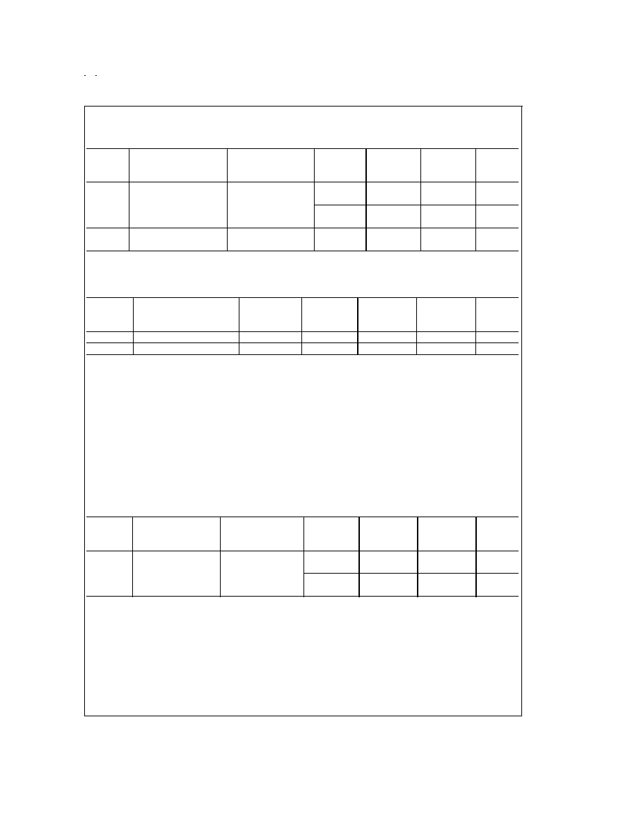
Connection Diagrams
Ordering Information
Package
Ordering
NSC Drawing
Package
Transport Media
Information
Number
Marking
8-Pin DIP
LMC7111AIN
N08E
LMC7111AIN
Rails
8-Pin DIP
LMC7111BIN
N08E
LMC7111BIN
Rails
5-Pin SOT23-5
LMC7111BIM5
MA05A
A01B
1k units Tape and Reel
LMC7111BIM5X MA05A
A01B
3k Units Tape and Reel
8-Pin DIP
DS012352-1
Top View
5-Pin SOT23-5
DS012352-2
Top View
Actual Size
DS012352-19
August 1999
LMC71
1
1
T
iny
CMOS
Operational
Amplifier
with
Rail-to-Rail
Input
and
Output
© 1999 National Semiconductor Corporation
DS012352
www.national.com

Absolute Maximum Ratings
(Note 1)
If Military/Aerospace specified devices are required,
please contact the National Semiconductor Sales Office/
Distributors for availability and specifications.
ESD Tolerance SOT23-5 (Note 2)
2000V
ESD Tolerance DIP Package
(Note 2)
1500V
Differential Input Voltage
±
Supply Voltage
Voltage at Input/Output Pin
(V
+
) + 0.3V, (V
-
) - 0.3V
Supply Voltage (V
+
- V
-
)
11V
Current at Input Pin
±
5 mA
Current at Output Pin (Note 3)
±
30 mA
Current at Power Supply Pin
30 mA
Lead Temp. (Soldering, 10 sec.)
260∞C
Storage Temperature Range
-65∞C to +150∞C
Junction Temperature (Note 4)
150∞C
Operating Ratings
(Note 1)
Supply Voltage
2.5V
V
+
11V
Junction Temperature Range
LMC7111AI, LMC7111BI
-40∞C
T
J
+85∞C
Thermal Resistance (
JA
)
N Package, 8-Pin Molded DIP
115∞C/W
M05A Package,
5-Pin Surface Mount
325∞C/W
2.7V DC Electrical Characteristics
Unless otherwise specified, all limits guaranteed for T
J
= 25∞C, V
+
= 2.7V, V
-
= 0V, V
CM
= V
O
= V
+
/2 and R
L
>
1 M
. Bold-
face limits apply at the temperature extremes.
Typ
LMC7111AI
LMC7111BI
Symbol
Parameter
Conditions
(Note 5)
Limit
Limit
Units
(Note 6)
(Note 6)
V
OS
Input Offset Voltage
V
+
= 2.7V
0.9
3
7
mV
5
9
max
TCV
OS
Input Offset Voltage
2.0
µV/∞C
Average Drift
I
B
Input Bias Current
(Note 9)
0.1
1
1
pA
20
20
max
I
OS
Input Offset Current
(Note 9)
0.01
0.5
0.5
pA
10
10
max
R
IN
Input Resistance
>
10
Tera
+PSRR
Positive Power Supply
2.7V
V
+
5.0V,
60
55
55
dB
Rejection Ratio
V
-
= 0V, V
O
= 2.5V
50
50
min
-PSRR
Negative Power Supply
-2.7V
V
-
-5.0V,
60
55
55
dB
Rejection Ratio
V
-
= 0V, V
O
= 2.5V
50
50
min
V
CM
Input Common-Mode
V
+
= 2.7V
-0.10
0.0
0.0
V
Voltage Range
For CMRR
50 dB
0.40
0.40
min
2.8
2.7
2.7
V
2.25
2.25
max
C
IN
Common-Mode Input
3
pF
Capacitance
V
O
Output Swing
V
+
= 2.7V
2.69
2.68
2.68
V
R
L
= 100 k
2.4
2.4
min
0.01
0.02
0.02
V
0.08
0.08
max
V
+
= 2.7V
2.65
2.6
2.6
V
R
L
= 10 k
2.4
2.4
min
0.03
0.1
0.1
V
0.3
0.3
max
I
SC
Output Short Circuit
Sourcing, V
O
= 0V
7
1
1
mA
Current
0.7
0.7
min
Sinking, V
O
= 2.7V
7
1
1
mA
0.7
0.7
min
www.national.com
2
2.7V DC Electrical Characteristics
(Continued)
Unless otherwise specified, all limits guaranteed for T
J
= 25∞C, V
+
= 2.7V, V
-
= 0V, V
CM
= V
O
= V
+
/2 and R
L
>
1 M
. Bold-
face limits apply at the temperature extremes.
Typ
LMC7111AI
LMC7111BI
Symbol
Parameter
Conditions
(Note 5)
Limit
Limit
Units
(Note 6)
(Note 6)
A
VOL
Voltage Gain
Sourcing
400
V/mv
min
Sinking
150
V/mv
min
I
S
Supply Current
V
+
= +2.7V,
20
45
50
µA
V
O
= V
+
/2
60
65
max
2.7V AC Electrical Characteristics
Unless otherwise specified, all limits guaranteed for T
J
= 25∞C, V
+
= 2.7V, V
-
= 0V, V
CM
= V
O
= V
+
/2 and R
L
>
1 M
. Bold-
face limits apply at the temperature extremes.
Typ
LMC7111AI
LMC7111BI
Symbol
Parameter
Conditions
(Note 5)
Limit
Limit
Units
(Note 6)
(Note 6)
SR
Slew Rate
(Note 8)
0.015
V/µs
GBW
Gain-Bandwidth Product
40
kHz
Note 1: Absolute Maximum Ratings indicate limits beyond which damage to the device may occur. Operating Ratings indicate conditions for which the device is in-
tended to be functional, but specific performance is not guaranteed. For guaranteed specifications and the test conditions, see the Electrical Characteristics.
Note 2: Human body model, 1.5 k
in series with 100 pF.
Note 3: Applies to both single-supply and split-supply operation. Continuous short circuit operation at elevated ambient temperature can result in exceeding the
maximum allowed junction temperature at 150∞C.
Note 4: The maximum power dissipation is a function of T
J(max)
,
JA
and T
A
. The maximum allowable power dissipation at any ambient temperature is P
D
= (T
J(max)
- T
A
)/
JA
. All numbers apply for packages soldered directly into a PC board.
Note 5: Typical Values represent the most likely parametric norm.
Note 6: All limits are guaranteed by testing or statistical analysis.
Note 7: V
+
= 2.7V, V
CM
= 1.35V and R
L
connected to 1.35V. For Sourcing tests, 1.35V
V
O
2.7V. For Sinking tests, 0.5V
V
O
1.35V.
Note 8: Connected as Voltage Follower with 1.0V step input. Number specified is the slower of the positive and negative slew rates. Input referred, V
+
= 2.7V and
R
L
= 100 k
connected to 1.35V. Amp excited with 1 kHz to produce V
O
= 1 V
PP
.
Note 9: Bias Current guaranteed by design and processing.
3V DC Electrical Characteristics
Unless otherwise specified, all limits guaranteed for T
J
= 25∞C, V
+
= 3V, V
-
= 0V, V
CM
= V
O
= V
+
/2 and R
L
>
1 M
. Bold-
face limits apply at the temperature extremes.
Typ
LMC7111AI
LMC7111BI
Symbol
Parameter
Conditions
(Note 5)
Limit
Limit
Units
(Note 6)
(Note 6)
V
CM
Input Common-Mode
V
+
= 3V
-0.25
0.0
0.0
V
Voltage Range
For CMRR
50 dB
min
3.2
3.0
3.0
V
2.8
2.8
max
www.national.com
3

3.3V DC Electrical Characteristics
Unless otherwise specified, all limits guaranteed for T
J
= 25∞C, V
+
= 3.3V, V
-
= 0V, V
CM
= V
O
= V
+
/2 and R
L
>
1 M
. Bold-
face limits apply at the temperature extremes.
Typ
LMC7111AI
LMC7111BI
Symbol
Parameter
Conditions
(Note 5)
Limit
Limit
Units
(Note 6)
(Note 6)
V
CM
Input Common-Mode
V
+
= 3.3V
-0.25
-0.1
-0.1
V
Voltage Range
For CMRR
50 dB
0.00
0.00
min
3.5
3.4
3.4
V
3.2
3.2
max
5V DC Electrical Characteristics
Unless otherwise specified, all limits guaranteed for T
J
= 25∞C, V
+
= 5V, V
-
= 0V, V
CM
= V
O
= V
+
/2 and R
L
>
1 M
. Bold-
face limits apply at the temperature extremes.
Typ
LMC7111AI
LMC7111BI
Symbol
Parameter
Conditions
(Note 5)
Limit
Limit
Units
(Note 6)
(Note 6)
V
OS
Input Offset Voltage
V
+
= 5V
0.9
mV
max
TCV
OS
Input Offset Voltage
2.0
µV/∞C
Average Drift
I
B
Input Bias Current
(Note 9)
0.1
1
1
pA
20
20
max
I
OS
Input Offset Current
(Note 9)
0.01
0.5
0.5
pA
10
10
max
R
IN
Input Resistance
>
10
Tera
CMRR
Common Mode
0V
V
CM
5V
85
70
60
dB
Rejection Ratio
min
+PSRR
Positive Power Supply
5V
V
+
10V,
85
70
60
dB
Rejection Ratio
V
-
= 0V, V
O
= 2.5V
min
-PSRR
Negative Power Supply
-5V
V
-
-10V,
85
70
60
dB
Rejection Ratio
V
-
= 0V, V
O
= -2.5V
min
V
CM
Input Common-Mode
V
+
= 5V
-0.3
-0.20
-0.20
V
Voltage Range
For CMRR
50 dB
0.00
0.00
min
5.25
5.20
5.20
V
5.00
5.00
max
C
IN
Common-Mode Input
3
pF
Capacitance
V
O
Output Swing
V
+
= 5V
4.99
4.98
4.98
Vmin
R
L
= 100 k
0.01
0.02
0.02
Vmax
V
+
= 5V
4.98
4.9
4.9
Vmin
R
L
= 10 k
0.02
0.1
0.1
Vmin
I
SC
Output Short Circuit
Sourcing, V
O
= 0V
7
5
5
mA
Current
3.5
3.5
min
Sinking, V
O
= 3V
7
5
5
mA
3.5
3.5
min
A
VOL
Voltage Gain
Sourcing
500
V/mv
min
Sinking
200
V/mv
min
I
S
Supply Current
V
+
= +5V,
25
µA
V
O
= V
+
/2
max
www.national.com
4
5V AC Electrical Characteristics
Unless otherwise specified, all limits guaranteed for T
J
= 25∞C, V
+
= 5V, V
-
= 0V, V
CM
= V
O
= V
+
/2 and R
L
>
1 M
. Bold-
face limits apply at the temperature extremes.
Typ
LMC7111AI
LMC7111BI
Symbol
Parameter
Conditions
(Note 5)
Limit
Limit
Units
(Note 6)
(Note 6)
SR
Slew Rate
Positive Going Slew Rate
0.027
0.015
0.010
V/µs
(Note 8)
GBW
Gain-Bandwidth Product
50
kHz
Note 10: Absolute Maximum Ratings indicate limits beyond which damage to the device may occur. Operating Ratings indicate conditions for which the device is
intended to be functional, but specific performance is not guaranteed. For guaranteed specifications and the test conditions, see the Electrical Characteristics.
Note 11: Human body model, 1.5 k
in series with 100 pF.
Note 12: Applies to both single-supply and split-supply operation. Continuous short circuit operation at elevated ambient temperature can result in exceeding the
maximum allowed junction temperature at 150∞C.
Note 13: The maximum power dissipation is a function of T
J(max)
,
JA
and T
A
. The maximum allowable power dissipation at any ambient temperature is P
D
= (T
J(max)
- T
A
)/
JA
. All numbers apply for packages soldered directly into a PC board.
Note 14: Typical Values represent the most likely parametric norm.
Note 15: All limits are guaranteed by testing or statistical analysis.
Note 16: V
+
= 5V, V
CM
= 2.5V and R
L
connected to 2.5V. For Sourcing tests, 2.5V
V
O
5.0V. For Sinking tests, 0.5V
V
O
2.5V.
Note 17: Connected as Voltage Follower with 1.0V step input. Number specified is the slower of the positive slew rate. The negative slew rate is faster. Input referred,
V
+
= 5V and R
L
= 100 k
connected to 1.5V. Amp excited with 1 kHz to produce V
O
= 1 V
PP
.
Note 18: Bias Current guaranteed by design and processing.
10V DC Electrical Characteristics
Unless otherwise specified, all limits guaranteed for T
J
= 25∞C, V
+
= 10V, V
-
= 0V, V
CM
= V
O
= V
+
/2 and R
L
>
1 M
. Bold-
face limits apply at the temperature extremes.
Typ
LMC7111AI
LMC7111BI
Symbol
Parameter
Conditions
(Note 5)
Limit
Limit
Units
(Note 6)
(Note 6)
V
OS
Input Offset Voltage
V
+
= 10V
0.9
3
7
mV
5
9
max
TCV
OS
Input Offset Voltage
2.0
µV/∞C
Average Drift
I
B
Input Bias Current
0.1
1
1
pA
20
20
max
I
OS
Input Offset Current
0.01
0.5
0.5
pA
10
10
max
R
IN
Input Resistance
>
10
Tera
+PSRR
Positive Power Supply
5V
V
+
10V,
80
dB
Rejection Ratio
V
-
= 0V, V
O
= 2.5V
min
-PSRR
Negative Power Supply
-5V
V
-
-10V,
80
dB
Rejection Ratio
V
-
= 0V, V
O
= 2.5V
min
V
CM
Input Common-Mode
V
+
= 10V
-0.2
-0.15
-0.15
V
Voltage Range
For CMRR
50 dB
0.00
0.00
min
10.2
10.15
10.15
V
10.00
10.00
max
C
IN
Common-Mode Input
3
pF
Capacitance
I
SC
Output Short Circuit
Sourcing, V
O
= 0V
30
20
20
mA
Current (Note 9)
7
7
min
Sinking, V
O
= 10V
30
20
20
mA
7
7
min
www.national.com
5