 | –≠–ª–µ–∫—Ç—Ä–æ–Ω–Ω—ã–π –∫–æ–º–ø–æ–Ω–µ–Ω—Ç: LMC7660 | –°–∫–∞—á–∞—Ç—å:  PDF PDF  ZIP ZIP |

LMC7660
Switched Capacitor Voltage Converter
General Description
The LMC7660 is a CMOS voltage converter capable of con-
verting a positive voltage in the range of +1.5V to +10V to
the corresponding negative voltage of -1.5V to -10V. The
LMC7660
is
a
pin-for-pin
replacement
for
the
industry-standard 7660. The converter features: operation
over full temperature and voltage range without need for an
external diode, low quiescent current, and high power effi-
ciency.
The LMC7660 uses its built-in oscillator to switch 4 power
MOS switches and charge two inexpensive electrolytic ca-
pacitors.
Features
n
Operation over full temperature and voltage range
without an external diode
n
Low supply current, 200 µA max
n
Pin-for-pin replacement for the 7660
n
Wide operating range 1.5V to 10V
n
97% Voltage Conversion Efficiency
n
95% Power Conversion Efficiency
n
Easy to use, only 2 external components
n
Extended temperature range
n
Narrow SO-8 Package
Block Diagram
Pin Configuration
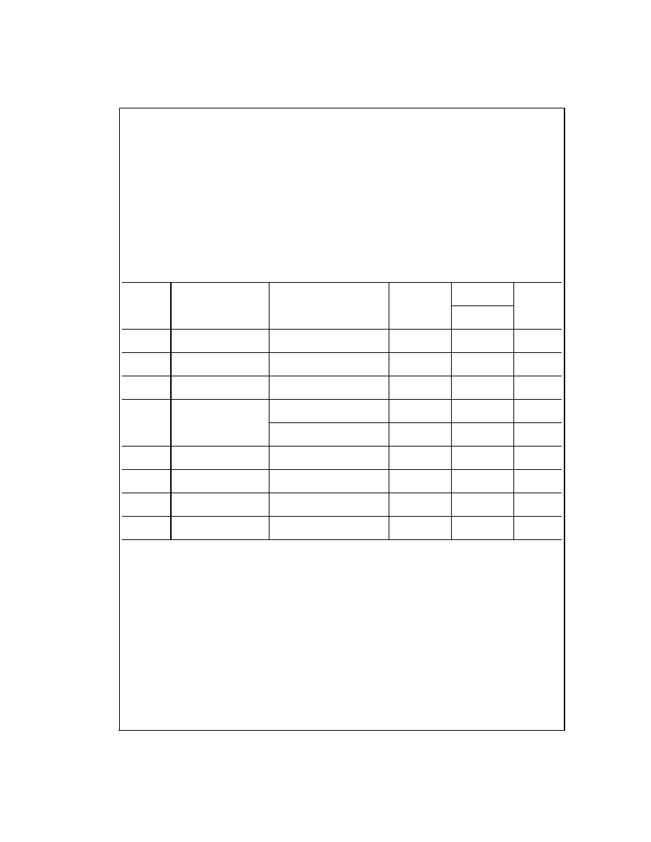
Ordering Information
Package
Temperature Range
NSC
Drawing
Industrial
-40∞C to +85∞C
8-Lead Molded DIP
LMC7660IN
N08E
8-Lead Molded Small Outline
LMC7660IM
M08A
DS009136-1
DS009136-2
April 1997
LMC7660
Switched
Capacitor
V
oltage
Converter
© 1997 National Semiconductor Corporation
DS009136
www.national.com
Absolute Maximum Ratings
(Note 1)
If Military/Aerospace specified devices are required,
please contact the National Semiconductor Sales Office/
Distributors for availability and specifications.
Supply Voltage
10.5V
Input Voltage on Pin 6, 7
(Note 2)
-0.3V to (V
+
+ 0.3V)
for V
+
<
5.5V
(V
+
- 5.5V) to (V
+
+ 0.3V)
for V
+
>
5.5V
Current into Pin 6 (Note 2)
20 µA
Output Short Circuit
Duration (V
+
5.5V)
Continuous
Power Dissipation (Note 3)
Dual-In-Line Package
1.4W
Surface-Mount Package
0.6W
T
J
Max (Note 3)
150∞C
JA
(Note 3)
Dual-In-Line Package
90∞C/W
Surface-Mount Package
160∞C/W
Storage Temp. Range
-65∞C
T
150∞C
Lead Temperature
(Soldering, 5 sec.)
260∞C
ESD Tolerance (Note 7)
±
2000V
Electrical Characteristics
(Note 4)
Symbol
Parameter
Conditions
Typ
LMC7660IN/
Units
Limits
LMC7660IM
Limit
(Note 5)
I
s
Supply Current
R
L
=
120
200
µA
400
max
V
+
H
Supply Voltage
R
L
= 10 k
, Pin 6 Open
3 to 10
3 to 10
V
Range High (Note 6)
Voltage Efficiency
90%
3 to 10
V
+
L
Supply Voltage
R
L
= 10 k
, Pin 6 to Gnd.
1.5 to 3.5
1.5 to 3.5
V
Range Low
Voltage Efficiency
90%
1.5 to 3.5
R
out
Output Source
I
L
= 20 mA
55
100
Resistance
120
max
V = 2V, I
L
= 3 mA
110
200
Pin 6 Short to Gnd.
300
max
F
osc
Oscillator
10
kHz
Frequency
P
eff
Power Efficiency
R
L
= 5 k
97
95
%
90
min
V
o eff
Voltage Conversion
R
L
=
99.9
97
%
Efficiency
95
min
I
osc
Oscillator Sink or
Pin 7 = Gnd. or V
+
3
µA
Source Current
Note 1: Absolute Maximum ratings indicate limits beyond which damage to the device may occur. DC and AC electrical specifications do not apply when operating
the device beyond its rated operating conditions. See Note 4 for conditions.
Note 2: Connecting any input terminal to voltages greater than V
+
or less than ground may cause destructive latchup. It is recommended that no inputs from sources
operating from external supplies be applied prior to "power-up" of the LMC7660.
Note 3: For operation at elevated temperature, these devices must be derated based on a thermal resistance of
ja
and T
j
max, T
j
= T
A
+
ja
P
D
.
Note 4: Boldface numbers apply at temperature extremes. All other numbers apply at T
A
= 25∞C, V
+
= 5V, C
osc
= 0, and apply for the LMC7660 unless otherwise
specified. Test circuit is shown in
Figure 1 .
Note 5: Limits at room temperature are guaranteed and 100% production tested. Limits in boldface are guaranteed over the operating temperature range (but not
100% tested), and are not used to calculate outgoing quality levels.
Note 6: The LMC7660 can operate without an external diode over the full temperature and voltage range. The LMC7660 can also be used with the external diode
Dx, when replacing previous 7660 designs.
Note 7: The test circuit consists of the human body model of 100 pF in series with 1500
.
www.national.com
2

Electrical Characteristics
(Note 4) (Continued)
Typical Performance Characteristics
DS009136-5
FIGURE 1. LMC7660 Test Circuit
OSC Freq. vs OSC
Capacitance
DS009136-18
V
out
vs I
out
@
V
+
= 2V
DS009136-19
V
out
vs I
out
@
V
+
= 5V
DS009136-20
Supply Current & Power Efficiency
vs Load Current (V
+
= 2V)
DS009136-21
Supply Current & Power Efficiency
vs Load Current (V
+
= 5V)
DS009136-22
Output Source Resistiance as a
Function of Temperature
DS009136-23
3
www.national.com

Typical Performance Characteristics
(Continued)
Application Information
Circuit Description
The LMC7660 contains four large CMOS switches which are
switched in a sequence to provide supply inversion V
out
=
-V
in
. Energy transfer and storage are provided by two inex-
pensive electrolytic capacitors.
Figure 2 shows how the
LMC7660 can be used to generate -V
+
from V
+
. When
switches S1 and S3 are closed, C
p
charges to the supply
voltage V
+
. During this time interval, switches S2 and S4 are
open. After C
p
charges to V
+
, S1 and S3 are opened, S2 and
S4 are then closed. By connecting S2 to ground, C
p
devel-
ops a voltage -V
+
/2 on C
r
. After a number of cycles C
r
will be
pumped to exactly -V
+
. This transfer will be exact assuming
no load on C
r
, and no loss in the switches.
In the circuit of
Figure 2, S1 is a P-channel device and S2,
S3, and S4 are N-channel devices. Because the output is bi-
ased below ground, it is important that the p
-
wells of S3 and
S4 never become forward biased with respect to either their
sources or drains. A substrate logic circuit guarantees that
these p
-
wells are always held at the proper voltage. Under
all conditions S4 p
-
well must be at the lowest potential in the
circuit. To switch off S4, a level translator generates V
GS4
=
0V, and this is accomplished by biasing the level translator
from the S4 p
-
well.
An internal RC oscillator and ˜ 2 circuit provide timing sig-
nals to the level translator. The built-in regulator biases the
oscillator and divider to reduce power dissipation on high
supply voltage. The regulator becomes active at about V
+
=
6.5V. Low voltage operation can be improved if the LV pin is
shorted to ground for V
+
3.5V. For V
+
3.5V, the LV pin
must be left open to prevent damage to the part.
Power Efficiency and Ripple
It is theoretically possible to approach 100% efficiency if the
following conditions are met:
1. The drive circuitry consumes little power.
2. The power switches are matched and have low R
on
.
3. The impedance of the reservoir and pump capacitors are
negligibly small at the pumping frequency.
The LMC7660 closely approaches 1 and 2 above. By using
a large pump capacitor C
p
, the charge removed while sup-
plying the reservoir capacitor is small compared to C
p
's total
charge. Small removed charge means small changes in the
pump capacitor voltage, and thus small energy loss and high
efficiency. The energy loss by C
p
is:
By using a large reservoir capacitor, the output ripple can be
reduced to an acceptable level. For example, if the load cur-
rent is 5 mA and the accepted ripple is 200 mV, then the res-
ervoir capacitor can omit approximately be calculated from:
Precautions
1. Do not exceed the maximum supply voltage or junction
temperature.
2. Do not short pin 6 (LV terminal) to ground for supply volt-
ages greater than 3.5V.
3. Do not short circuit the output to V
+
.
4. External electrolytic capacitors C
r
and C
p
should have
their polarities connected as shown in
Figure 1.
Replacing Previous 7660 Designs
To prevent destructive latchup, previous 7660 designs re-
quire a diode in series with the output when operated at el-
evated temperature or supply voltage. Although this pre-
vented the latchup problem of these designs, it lowered the
available output voltage and increased the output series re-
sistance.
The National LMC7660 has been designed to solve the in-
herent latch problem. The LCM7660 can operate over the
entire supply voltage and temperature range without the
need for an output diode. When replacing existing designs,
the LMC7660 can be operated with diode Dx.
Unloaded Oscillator Frequency
as a Function of Temperature
DS009136-24
Output R vs Supply Voltage
DS009136-25
P
eff
vs OSC Freq.
@
V
+
= 5V
DS009136-26
www.national.com
4

Application Information
(Continued)
Typical Applications
Changing Oscillator Frequency
It is possible to dramatically reduce the quiescent operating
current of the LMC7660 by lowering the oscillator frequency.
The oscillator frequency can be lowered from a nominal 10
kHz to several hundred hertz, by adding a slow-down ca-
pacitor C
osc
(
Figure 3). As shown in the Typical Performance
Curves the supply current can be lowered to the 10 µA
range. This low current drain can be extremely useful when
used in µPower and battery back-up equipment. It must be
understood that the lower operating frequency and supply
current cause an increased impedance of C
r
and C
p
. The in-
creased impedance, due to a lower switching rate, can be
offset by raising C
r
and C
p
until ripple and load current re-
quirements are met.
Synchronizing to an External Clock
Figure 4 shows an LMC7660 synchronized to an external
clock. The CMOS gate overrides the internal oscillator when
it is necessary to switch faster or reduce power supply inter-
ference. The external clock still passes through the ˜2 circuit
in the 7660, so the pumping frequency will be
1
/
2
the external
clock frequency.
Lowering Output Impedance
Paralleling two or more LMC7660's lowers output imped-
ance. Each device must have it's own pumping capacitor C
p
,
but the reservoir capacitor C
r
is shared as depicted in
Figure
5. The composite output resistance is:
DS009136-6
FIGURE 2. Idealized Voltage Converter
DS009136-7
FIGURE 3. Reduce Supply Current by Lowering Oscillator Frequency
DS009136-8
FIGURE 4. Synchronizing to an External Clock
5
www.national.com