 | ÐлекÑÑоннÑй компоненÑ: LMH6639MF | СкаÑаÑÑ:  PDF PDF  ZIP ZIP |
Äîêóìåíòàöèÿ è îïèñàíèÿ www.docs.chipfind.ru
LMH6639
190MHz Rail-to-Rail Output Amplifier with Disable
General Description
The LMH6639 is a voltage feedback operational amplifier
with a rail-to-rail output drive capability of 110mA. Employing
National's patented VIP10 process, the LMH6639 delivers a
bandwidth of 190MHz at a current consumption of only
3.6mA. An input common mode voltage range extending to
0.2V below the V
-
and to within 1V of V
+
, makes the
LMH6639 a true single supply op-amp. The output voltage
range extends to within 30mV of either supply rail providing
the user with a dynamic range that is especially desirable in
low voltage applications.
The LMH6639 offers a slew rate of 172V/µs resulting in a full
power bandwidth of approximately 28MHz. The T
ON
value of
83nsec combined with a settling time of 33nsec makes this
device ideally suited for multiplexing applications. Careful
attention has been paid to ensure device stability under all
operating voltages and modes. The result is a very well
behaved frequency response characteristic for any gain set-
ting including +1, and excellent specifications for driving
video cables including harmonic distortion of -60dBc, differ-
ential gain of 0.12% and differential phase of 0.045°
Features
(V
S
= 5V, Typical values unless specified)
n
Supply current (no load)
3.6mA
n
Supply current (off mode)
400µA
n
Output resistance (closed loop 1MHz)
0.186
n
-3dB BW (A
V
= 1)
190MHz
n
Settling time
33nsec
n
Input common mode voltage
-0.2V to 4V
n
Output voltage swing
40mV from rails
n
Linear output current
110mA
n
Total harmonic distortion
-60dBc
n
Fully characterized for 3V, 5V and
±
5V
n
No output phase reversal with CMVR exceeded
n
Excellent overdrive recovery
n
Off Isolation 1MHz
-70dB
n
Differential Gain
0.12%
n
Differential Phase
0.045°
Applications
n
Active filters
n
CD/DVD ROM
n
ADC buffer amplifier
n
Portable video
n
Current sense buffer
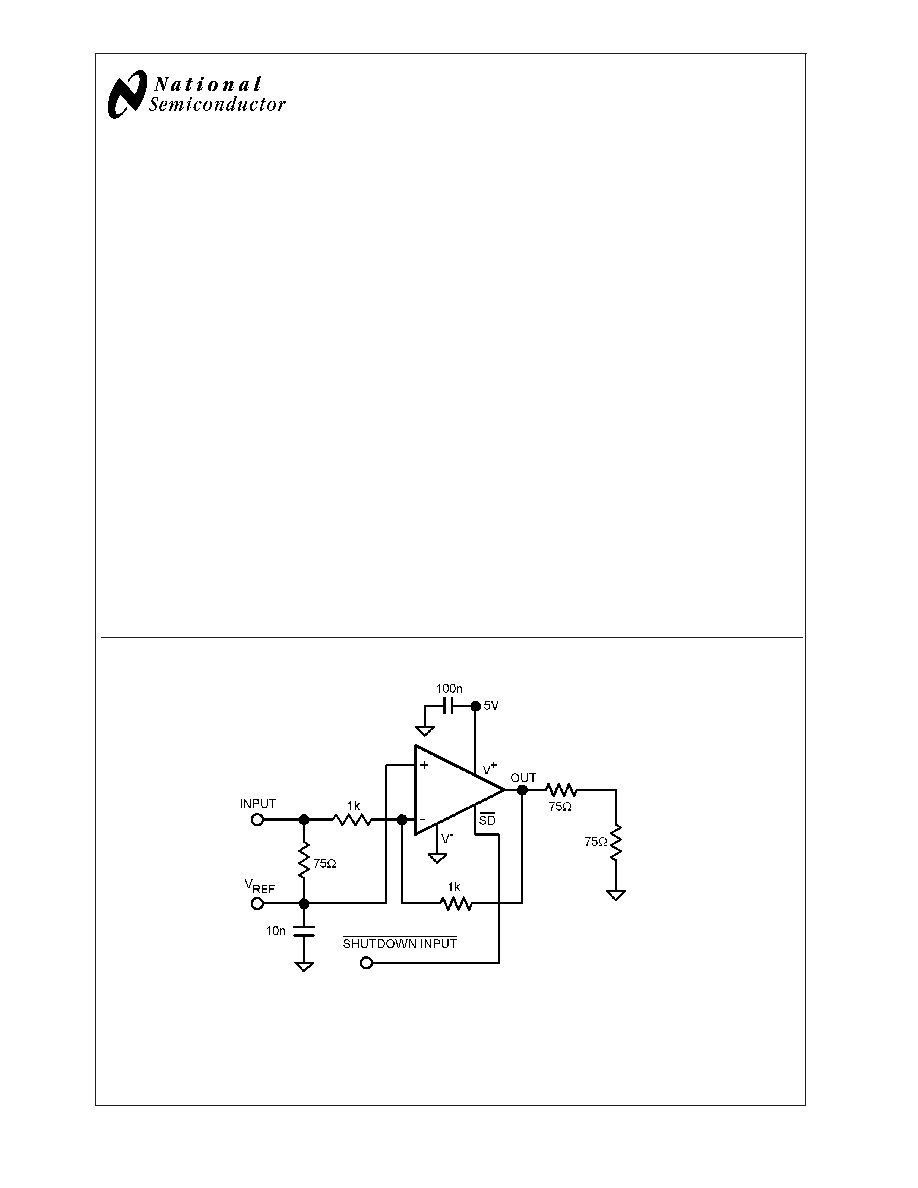
20030246
FIGURE 1. Typical Single Supply Schematic
July 2003
LMH6639
190MHz
Rail-to-Rail
Output
Amplifier
with
Disable
© 2003 National Semiconductor Corporation
DS200302
www.national.com
Absolute Maximum Ratings
(Note 1)
If Military/Aerospace specified devices are required,
please contact the National Semiconductor Sales Office/
Distributors for availability and specifications.
ESD Tolerance
2KV (Note 2)
200V (Note 9)
V
IN
Differential
±
2.5V
Input Current
±
10mA
Supply Voltage (V
+
V
-
)
13.5V
Voltage at Input/Output pins
V
+
+0.8V, V
-
-0.8V
Storage Temperature Range
-65°C to +150°C
Junction Temperature (Note 4)
+150°C
Soldering Information
Infrared or Convection (20 sec)
235°C
Wave Soldering (10 sec)
260°C
Operating Ratings
(Note 1)
Operating Temperature Range (Note 4)
-40°C to +85°C
Package Thermal Resistance (
JA
) (Note 4)
SOT23-6
265°C/W
SOIC-8
190°C/W
3V Electrical Characteristics
Unless otherwise specified, all limits guaranteed for at T
J
= 25°C, V
+
= 3V, V
-
= 0V, V
O
= V
CM
= V
+
/2, and R
L
= 2k
to V
+
/2.
Boldface limits apply at the temperature extremes.
Symbol
Parameter
Conditions
Min
(Note 6)
Typ
(Note 5)
Max
(Note 6)
Units
BW
-3dB BW
A
V
= +1
120
170
MHz
A
V
= -1
63
BW
0.1dB
0.1dB Gain Flatness
R
F
= 2.65k
, R
L
= 1k
,
16.4
MHz
FPBW
Full Power Bandwidth
A
V
= +1, V
OUT
= 2V
PP
, -1dB
V
+
= 1.8V, V
-
= 1.2V
21
MHz
GBW
Gain Bandwidth product
A
V
= +1
83
MHz
e
n
Input-Referred Voltage Noise
R
F
= 33k
f = 10kHz
19
nV/
f = 1MHz
16
i
n
Input-Referred Current Noise
R
F
= 1M
f = 10kHz
1.30
pA/
f = 1MHz
0.36
THD
Total Harmonic Distortion
f = 5MHz, V
O
= 2V
PP
, A
V
= +2,
R
L
= 1k
to V
+
/2
-50
dBc
T
S
Settling Time
V
O
= 2V
PP
,
±
0.1%
37
ns
SR
Slew Rate
A
V
= -1 (Note 8)
120
167
V/µs
V
OS
Input Offset Voltage
1.01
5
7
mV
TC V
OS
Input Offset Average Drift
(Note 11)
8
µV/°C
I
B
Input Bias Current
(Note 7)
-1.02
-2.6
-3.5
µA
I
OS
Input Offset Current
20
800
1000
nA
R
IN
Common Mode Input
Resistance
A
V
= +1, f = 1kHz, R
S
= 1M
6.1
M
C
IN
Common Mode Input
Capacitance
A
V
= +1, R
S
= 100k
1.35
pF
CMVR
Input Common-Mode Voltage
Range
CMRR
50dB
-0.3
-0.2
-0.1
V
1.8
1.6
2
CMRR
Common Mode Rejection
Ratio
(Note 12)
72
93
dB
A
VOL
Large Signal Voltage Gain
V
O
= 2V
PP
, R
L
= 2k
to V
+
/2
80
76
100
dB
V
O
= 2V
PP
, R
L
= 150
to V
+
/2
74
70
78
LMH6639
www.national.com
2
3V Electrical Characteristics
(Continued)
Unless otherwise specified, all limits guaranteed for at T
J
= 25°C, V
+
= 3V, V
-
= 0V, V
O
= V
CM
= V
+
/2, and R
L
= 2k
to V
+
/2.
Boldface limits apply at the temperature extremes.
Symbol
Parameter
Conditions
Min
(Note 6)
Typ
(Note 5)
Max
(Note 6)
Units
V
O
Output Swing
High
R
L
= 2k
to V
+
/2, V
ID
= 200mV
2.90
2.98
V
R
L
= 150
to V
+
/2, V
ID
= 200mV
2.75
2.93
R
L
= 50
to V
+
/2, V
ID
= 200mV
2.6
2.85
Output Swing
Low
R
L
= 2k
to V
+
/2, V
ID
= -200mV
25
75
mV
R
L
= 150
to V
+
/2, V
ID
= -200mV
75
200
R
L
= 50
to V
+
/2, V
ID
= -200mV
130
300
I
SC
Output Short Circuit Current
Sourcing to V
+
/2, (Note 10)
50
35
120
mA
Sinking to V
+
/2, (Note 10)
67
40
140
I
OUT
Output Current
V
O
= 0.5V from either supply
99
mA
PSRR
Power Supply Rejection Ratio
(Note 12)
72
96
dB
I
S
Supply Current (Enabled)
No Load
3.5
5.6
7.5
mA
Supply Current (Disabled)
0.3
0.5
0.7
TH_SD
Threshold Voltage for
Shutdown Mode
V
+
-1.59
V
I_SD PIN
Shutdown Pin Input Current
SD Pin Connect to 0V (Note 7)
-13
µA
T
ON
On Time After Shutdown
83
nsec
T
OFF
Off Time to Shutdown
160
nsec
R
OUT
Output Resistance Closed
Loop
R
F
= 10k
, f = 1kHz, A
V
= -1
27
m
R
F
= 10k
, f = 1MHz, A
V
= -1
266
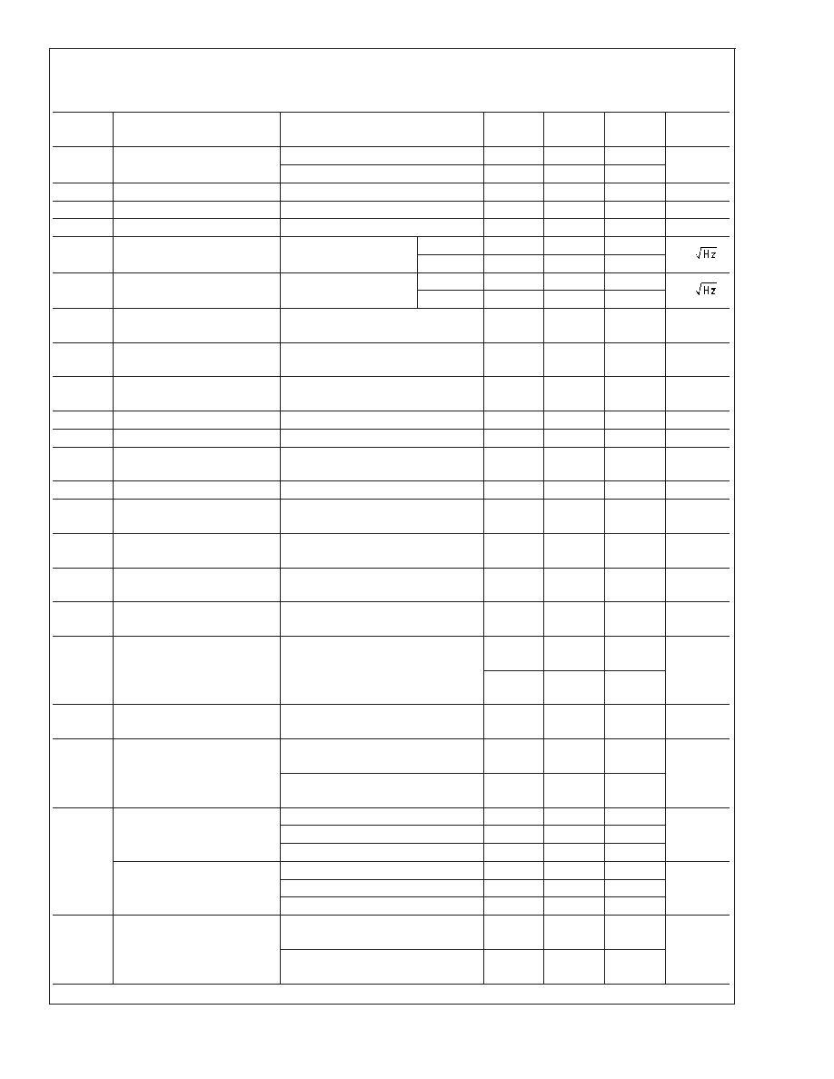
5V Electrical Characteristics
Unless otherwise specified, all limits guaranteed for at T
J
= 25°C, V
+
= 5V, V
-
= 0V, V
O
= V
CM
= V
+
/2, and R
L
= 2k
to V
+
/2.
Boldface limits apply at the temperature extremes.
Symbol
Parameter
Conditions
Min
(Note 6)
Typ
(Note 5)
Max
(Note 6)
Units
BW
-3dB BW
A
V
= +1
130
190
MHz
A
V
= -1
64
BW
0.1dB
0.1dB Gain Flatness
R
F
= 2.51k
, R
L
= 1k
,
16.4
MHz
FPBW
Full Power Bandwidth
A
V
= +1, V
OUT
= 2V
PP
, -1dB
28
MHz
GBW
Gain Bandwidth Product
A
V
= +1
86
MHz
e
n
Input-Referred Voltage Noise
R
F
= 33k
f = 10kHz
19
nV/
f = 1MHz
16
i
n
Input-Referred Current Noise
R
F
= 1M
f = 10KHz
1.35
pA/
f = 1MHz
0.35
THD
Total Harmonic Distortion
f = 5MHz, V
O
= 2V
PP
, A
V
= +2
R
L
= 1k
to V
+
/2
-60
dBc
DG
Differential Gain
NTSC, A
V
= +2
R
L
= 150
to V
+
/2
0.12
%
DP
Differential Phase
NTSC, A
V
= +2
R
L
= 150
to V
+
/2
0.045
deg
T
S
Settling Time
V
O
= 2V
PP
,
±
0.1%
33
ns
SR
Slew Rate
A
V
= -1, (Note 8)
130
172
V/µs
V
OS
Input Offset Voltage
1.02
5
7
mV
LMH6639
www.national.com
3
5V Electrical Characteristics
(Continued)
Unless otherwise specified, all limits guaranteed for at T
J
= 25°C, V
+
= 5V, V
-
= 0V, V
O
= V
CM
= V
+
/2, and R
L
= 2k
to V
+
/2.
Boldface limits apply at the temperature extremes.
Symbol
Parameter
Conditions
Min
(Note 6)
Typ
(Note 5)
Max
(Note 6)
Units
TC V
OS
Input Offset Average Drift
(Note 11)
8
µV/°C
I
B
Input Bias Current
(Note 7)
-1.2
-2.6
-3.25
µA
I
OS
Input Offset Current
20
800
1000
nA
R
IN
Common Mode Input
Resistance
A
V
= +1, f = 1kHz, R
S
= 1M
6.88
M
C
IN
Common Mode Input
Capacitance
A
V
= +1, R
S
= 100k
1.32
pF
CMVR
Common-Mode Input Voltage
Range
CMRR
50dB
-0.3
-0.2
-0.1
V
4
3.8
3.6
CMRR
Common Mode Rejection
Ratio
(Note 12)
72
95
dB
A
VOL
Large Signal Voltage Gain
V
O
= 4V
PP
R
L
= 2k
to V
+
/2
86
82
100
dB
V
O
= 3.75V
PP
R
L
= 150
to V
+
/2
74
70
77
V
O
Output Swing
High
R
L
= 2k
to V
+
/2, V
ID
= 200mV
4.90
4.97
V
R
L
= 150
to V
+
/2, V
ID
= 200mV
4.65
4.90
R
L
= 50
to V
+
/2, V
ID
= 200mV
4.40
4.77
Output Swing
Low
R
L
= 2k
to V
+
/2, V
ID
= -200mV
25
100
mV
R
L
= 150
to V
+
/2, V
ID
= -200mV
85
200
R
L
= 50
to V
+
/2, V
ID
= -200mV
190
400
I
SC
Output Short Circuit Current
Sourcing to V
+
/2, (Note 10)
100
79
160
mA
Sinking from V
+
/2, (Note 10)
120
85
190
I
OUT
Output Current
V
O
= 0.5V from either supply
110
mA
PSRR
Power Supply Rejection Ratio
(Note 12)
72
96
dB
I
S
Supply Current (Enabled)
No Load
3.6
5.8
8.0
mA
Supply Current (Disabled)
0.40
0.8
1.0
TH_SD
Threshold Voltage for
Shutdown Mode
V
+
-1.65
V
I_SD PIN
Shutdown Pin Input Current
SD Pin Connected to 0V (Note 7)
-30
µA
T
ON
On Time after Shutdown
83
nsec
T
OFF
Off Time to Shutdown
160
nsec
R
OUT
Output Resistance Closed
Loop
R
F
= 10k
, f = 1kHz, A
V
= -1
29
m
R
F
= 10k
, f = 1MHz, A
V
= -1
253
LMH6639
www.national.com
4
±
5V Electrical Characteristics
Unless otherwise specified, all limits guaranteed for at T
J
= 25°C, V
SUPPLY
=
±
5V, V
O
= V
CM
= GND, and R
L
= 2k
to V
+
/2.
Boldface limits apply at the temperature extremes.
Symbol
Parameter
Conditions
Min
(Note 6)
Typ
(Note 5)
Max
(Note 6)
Units
BW
-3dB BW
A
V
= +1
150
228
MHz
A
V
= -1
65
BW
0.1dB
0.1dB Gain Flatness
R
F
= 2.26k
, R
L
= 1k
18
MHz
FPBW
Full Power Bandwidth
A
V
= +1, V
OUT
= 2V
PP
, -1dB
29
MHz
GBW
Gain Bandwidth Product
A
V
= +1
90
MHz
e
n
Input-Referred Voltage Noise
R
F
= 33k
f = 10kHz
19
nV/
f = 1MHz
16
i
n
Input-Referred Current Noise
R
F
= 1M
f = 10kHz
1.13
pA/
f = 1MHz
0.34
THD
Total Harmonic Distortion
f = 5MHz, V
O
= 2V
PP
, A
V
= +2,
R
L
= 1k
-71.2
dBc
DG
Differential Gain
NTSC, A
V
= +2
R
L
= 150
0.11
%
DP
Differential Phase
NTSC, A
V
= +2
R
L
= 150
0.053
deg
T
S
Settling Time
V
O
= 2V
PP
,
±
0.1%
33
ns
SR
Slew Rate
A
V
= -1 (Note 8)
140
200
V/µs
V
OS
Input Offset Voltage
1.03
5
7
mV
TC V
OS
Input Offset Voltage Drift
(Note 11)
8
µV/°C
I
B
Input Bias Current
(Note 7)
-1.40
-2.6
-3.25
µA
I
OS
Input Offset Current
20
800
1000
nA
R
IN
Common Mode Input
Resistance
A
V
+1, f = 1kHz, R
S
= 1M
7.5
M
C
IN
Common Mode Input
Capacitance
A
V
= +1, R
S
= 100k
1.28
pF
CMVR
Common Mode Input Voltage
Range
CMRR
50dB
-5.3
-5.2
-5.1
V
3.8
3.6
4.0
CMRR
Common Mode Rejection
Ratio
(Note 12)
72
95
dB
A
VOL
Large Signal Voltage Gain
V
O
= 9V
PP
, R
L
= 2k
88
84
100
dB
V
O
= 8V
PP
, R
L
= 150
74
70
77
V
O
Output Swing
High
R
L
= 2k
, V
ID
= 200mV
4.85
4.96
V
R
L
= 150
, V
ID
= 200mV
4.55
4.80
R
L
= 50
, V
ID
= 200mV
3.60
4.55
Output Swing
Low
R
L
= 2k
, V
ID
= -200mV
-4.97
-4.90
V
R
L
= 150
, V
ID
= -200mV
-4.85
-4.55
R
L
= 50
, V
ID
= -200mV
-4.65
-4.30
I
SC
Output Short Circuit Current
Sourcing to Ground, (Note 10)
100
80
168
mA
Sinking to Ground, (Note 10)
110
85
190
LMH6639
www.national.com
5
Document Outline