
LMH6703
1.2 GHz, Low Distortion Op Amp with Shutdown
General Description
The LMH
TM
6703 is a very wideband, DC coupled monolithic
operational amplifier designed specifically for ultra high reso-
lution video systems as well as wide dynamic range systems
requiring exceptional signal fidelity. Benefiting from Nation-
al's current feedback architecture, the LMH6703 offers a
practical gain range of
±
1 to
±
10 while providing stable
operation without external compensation, even at unity gain.
At a gain of +2 the LMH6703 supports ultra high resolution
video systems with a 750 MHz 2 V
PP
-3 dB Bandwidth. With
12-bit distortion levels through 10 MHz (R
L
= 100
), and a
2.3nV/
input referred noise, the LMH6703 is the ideal
driver or buffer for high speed flash A/D and D/A converters.
Wide dynamic range systems such as radar and communi-
cation receivers requiring a wideband amplifier offering ex-
ceptional signal purity will find the LMH6703's low input
referred noise and low harmonic distortion an attractive so-
lution.
Features
n
-3 dB bandwidth (V
OUT
= 0.5 V
PP
, A
V
= +2)
1.2 GHz
n
2
nd
/3
rd
harmonics (20 MHz, SOT23-6)
-69/-90 dBc
n
Low noise
2.3nV/
n
Fast slew rate
4500 V/µs
n
Supply current
11 mA
n
Output current
90 mA
n
Low differential gain and phase
0.01%/0.02∞
Applications
n
RGB video driver
n
High resolution projectors
n
Flash A/D driver
n
D/A transimpedance buffer
n
Wide dynamic range IF amp
n
Radar/communication receivers
n
DDS post-amps
n
Line driver
Connection Diagrams
8-pin SOIC
6-pin SOT23
20110601
Top View
20110602
Top View
Ordering Information
Package
Part Number
Package Marking
Transport Media
NSC Drawing
8-Pin SOIC
LMH6703MA
LMH6703MA
95 Units/Rail
M08A
LMH6703MAX
2.5k Units Tape and Reel
6-Pin SOT23
LMH6703MF
AR1A
1k Units Tape and Reel
MF06A
LMH6703MFX
3k Units Tape and Reel
LMH
TM
is a trademark of National Semiconductor Corporation.
May 2005
LMH6703
1.2
GHz,
Low
Distortion
Op
Amp
with
Shutdown
© 2005 National Semiconductor Corporation
DS201106
www.national.com
Absolute Maximum Ratings
(Note 1)
If Military/Aerospace specified devices are required,
please contact the National Semiconductor Sales Office/
Distributors for availability and specifications.
ESD Tolerance (Note 5)
Human Body Model
2000V
Machine Model
200V
V
S
±
6.75V
I
OUT
(Note 3)
Common Mode Input Voltage
V
-
to V
+
Maximum Junction Temperature
+150∞C
Storage Temperature Range
-65∞C to +150∞C
Soldering Information
Infrared or Convection (20 sec.)
235∞C
Wave Soldering (10 sec.)
260∞C
Operating Ratings
(Note 1)
Operating Temperature Range
-40∞C to +85∞C
Supply Voltage Range
±
4V to
±
6V
Package Thermal Resistance (
JA
) (Note 4)
6-Pin SOT23
208∞C/W
8-Pin SOIC
160∞C/W
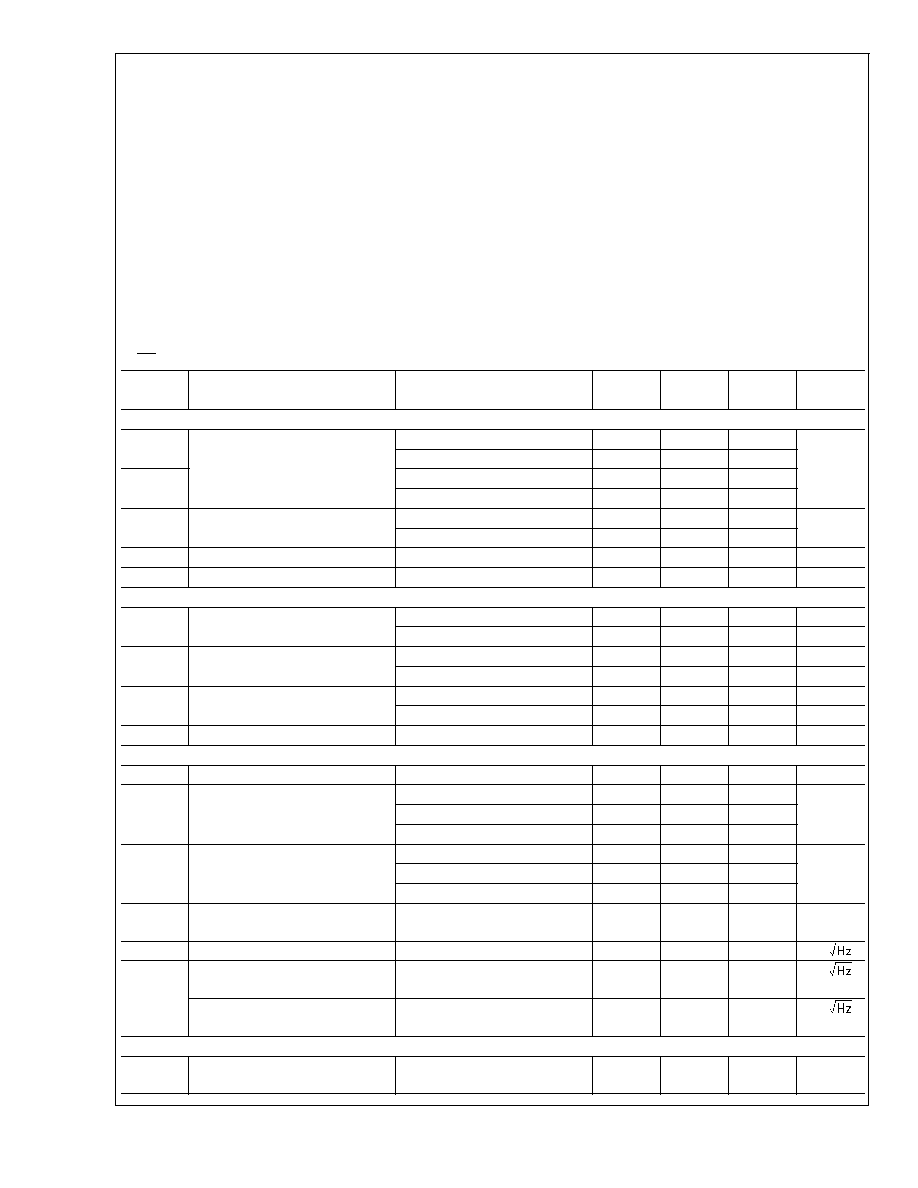
Electrical Characteristics
(Note 2)
Unless otherwise specified, all limits guaranteed for T
J
= 25∞C, A
V
= +2, V
S
=
±
5V, R
L
= 100
, R
F
= 560
,
SD = Floating. Boldface limits apply at the temperature extremes.
Symbol
Parameter
Conditions
Min
(Note 8)
Typ
(Note 7)
Max
(Note 8)
Units
Frequency Domain Performance
SSBW
-3 dB Bandwidth
V
OUT
= 0.5 V
PP
, A
V
= +1
1800
MHz
V
OUT
= 0.5 V
PP
, A
V
= +2
1200
LSBW
V
OUT
= 2 V
PP
750
V
OUT
= 4 V
PP
500
GF
0.1 dB Gain Flatness
V
OUT
= 0.5 V
PP
150
MHz
V
OUT
= 2 V
PP
150
DG
Differential Gain
R
L
= 150
, 4.43 MHz
0.01
%
DP
Differential Phase
R
L
= 150
, 4.43 MHz
0.02
deg
Time Domain Response
t
r
Rise Time
2V Step, 10% to 90%
0.5
ns
6V Step, 10% to 90%
1.05
ns
t
f
Fall Time
2V Step, 10% to 90%
0.5
ns
6V Step, 10% to 90%
1.05
ns
SR
Slew Rate
4V Step, 10% to 90% (Note 6)
4200
V/µs
6V Step, 10% to 90% (Note 6)
4500
V/µs
t
s
Settling Time
2V Step, V
OUT
within 0.1%
10
ns
Distortion And Noise Response
HD2
2
nd
Harmonic Distortion
2 V
PP
, 5 MHz, SOT23-6
-87
dBc
2 V
PP
, 20 MHz, SOT23-6
-69
2 V
PP
, 50 MHz, SOT23-6
-60
HD3
3
rd
Harmonic Distortion
2 V
PP
, 5 MHz, SOT23-6
-100
dBc
2 V
PP
, 20 MHz, SOT23-6
-90
2 V
PP
, 50 MHz, SOT23-6
-70
IMD
3
rd
Order Intermodulation
Products
50 MHz, P
O
= 5 dBm/ tone
-80
dBc
e
n
Input Referred Voltage Noise
>
1 MHz
2.3
nV/
i
n
Input Referred Noise Current
Inverting Pin
>
1 MHz
18.5
pA/
Input Referred Noise Current
Non-Inverting Pin
>
1 MHz
3
pA/
Static, DC Performance
V
OS
Input Offset Voltage
±
1.5
±
7
±
9
mV
LMH6703
www.national.com
2

Electrical Characteristics
(Note 2) (Continued)
Unless otherwise specified, all limits guaranteed for T
J
= 25∞C, A
V
= +2, V
S
=
±
5V, R
L
= 100
, R
F
= 560
,
SD = Floating. Boldface limits apply at the temperature extremes.
Symbol
Parameter
Conditions
Min
(Note 8)
Typ
(Note 7)
Max
(Note 8)
Units
TCV
OS
Input Offset Voltage Average Drift
(Note 10)
22
µV/∞C
I
B
Input Bias Current
Non-Inverting (Note 9)
-7
±
20
±
23
µA
Inverting (Note 9)
-2
±
35
±
44
TCI
B
Input Bias Current Average Drift
Non-Inverting (Note 10)
+30
nA/∞C
Inverting (Note 10)
-70
V
O
Output Voltage Range
R
L
=
±
3.3
±
3.45
V
R
L
= 100
±
3.2
±
3.14
±
3.4
PSRR
Power Supply Rejection Ratio
V
S
=
±
4.0V to
±
6.0V
48
46
52
dB
CMRR
Common Mode Rejection Ratio
V
CM
= -1.0V to +1.0V
45
44
47
dB
I
S
Supply Current (Enabled)
SD = 2V, R
L
=
11
12.5
15.0
mA
Supply Current (Disabled)
SD = 0.8V, R
L
=
0.2
0.900
0.935
mA
Miscellaneous Performance
R
IN+
Non-Inverting Input Resistance
1
M
R
IN-
Inverting Input Resistance
Output Impedance of Input
Buffer
30
C
IN
Non-Inverting Input Capacitance
0.8
pF
R
O
Output Resistance
Closed Loop
0.05
CMVR
Input Common Mode Voltage
Range
CMRR
40 dB
±
1.9
V
I
O
Linear Output Current
V
IN
= 0V, V
OUT
±
80 mV
±
55
±
90
mA
Enable/Disable Performance (Disabled Low)
T
ON
Enable Time
10
ns
T
OFF
Disable Time
10
ns
Output Glitch
50
mV
PP
V
IH
Enable Voltage
SD
V
IH
2.0
V
V
IL
Disable Voltage
SD
V
IL
0.8
V
I
IH
Disable Pin Bias Current, High
SD = V
+
(Note 9)
-7
±
70
µA
I
IL
Disable Pin Bias Current, Low
SD = 0V (Note 9)
-50
-240
-400
µA
I
OZ
Disabled Output Leakage Current
V
OUT
=
±
1.8V
0.07
±
25
±
40
µA
Note 1: Absolute Maximum Ratings indicate limits beyond which damage to the device may occur. Operating Ratings indicate conditions for which the device is
intended to be functional, but specific performance is not guaranteed. For guaranteed specifications, see the Electrical Characteristics tables.
Note 2: Electrical Table values apply only for factory testing conditions at the temperature indicated. Factory testing conditions result in very limited self-heating of
the device such that T
J
= T
A
. No guarantee of parametric performance is indicated in the electrical tables under conditions of internal self-heating where T
J
>
T
A
.
Note 3: The maximum output current (I
OUT
) is determined by device power dissipation limitations.
Note 4: The maximum power dissipation is a function of T
J(MAX)
,
JA
and T
A
. The maximum allowable power dissipation at any ambient temperature is P
D
=
(T
J(MAX)
-- T
A
)/
JA
. All numbers apply for package soldered directly into a 2 layer PC board with zero air flow.
Note 5: Human body model: 1.5 k
in series with 100 pF. Machine model: 0 in series with 200 pF.
Note 6: Slew Rate is the average of the rising and falling edges.
Note 7: Typical numbers are the most likely parametric norm.
Note 8: Limits are 100% production tested at 25∞C. Limits over the operating temperature range are guaranteed through correlation using Statistical Quality Control
(SQC) methods.
Note 9: Negative input current implies current flowing out of the device.
Note 10: Drift determined by dividing the change in parameter at temperature extremes by the total temperature change.
LMH6703
www.national.com
3
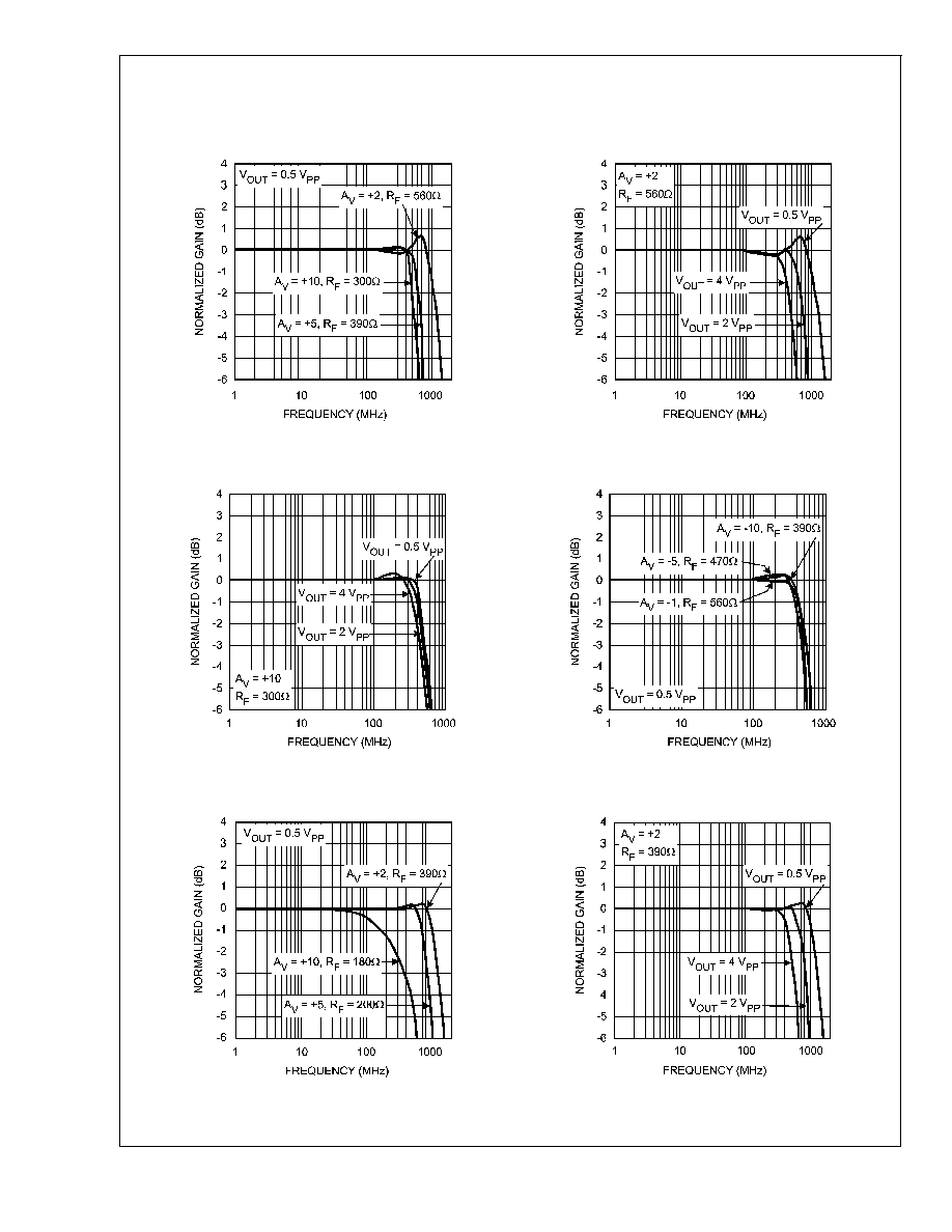
Typical Performance Characteristics
(A
V
= +2, R
L
= 100
, V
S
=
±
5V, R
F
= 560
, T
A
= +25∞C,
SOT23-6; unless otherwise specified).
Small Signal Non-Inverting Frequency Response
(SOT23)
Large Signal Frequency Response
(SOT23)
20110618
20110620
Large Signal Frequency Response
(SOT23)
Small Signal Inverting Frequency Response
(SOT23)
20110621
20110619
Small Signal Non-Inverting Frequency Response
(SOIC)
Large Signal Frequency Response
(SOIC)
20110615
20110616
LMH6703
www.national.com
4

Typical Performance Characteristics
(A
V
= +2, R
L
= 100
, V
S
=
±
5V, R
F
= 560
, T
A
= +25∞C,
SOT23-6; unless otherwise specified). (Continued)
Large Signal Frequency Response
(SOIC)
Small Signal Pulse Response
20110617
20110622
Large Signal Pulse Response
Harmonic Distortion vs. Frequency
20110623
20110624
Harmonic Distortion vs. Output Voltage
Harmonic Distortion vs. Load
20110627
20110625
LMH6703
www.national.com
5