 | –≠–ª–µ–∫—Ç—Ä–æ–Ω–Ω—ã–π –∫–æ–º–ø–æ–Ω–µ–Ω—Ç: LMH6715MA | –°–∫–∞—á–∞—Ç—å:  PDF PDF  ZIP ZIP |

LMH6715
Dual Wideband Video Op Amp
General Description
The LMH6715 combines National's VIP10
TM
high speed
complementary bipolar process with National's current feed-
back topology to produce a very high speed dual op amp.
The LMH6715 provides 400MHz small signal bandwidth at a
gain of +2V/V and 1300V/µs slew rate while consuming only
5.8mA per amplifier from
±
5V supplies.
The LMH6715 offers exceptional video performance with its
0.02% and 0.02∞ differential gain and phase errors for NTSC
and PAL video signals while driving up to four back termi-
nated 75
loads. The LMH6715 also offers a flat gain re-
sponse of 0.1dB to 100MHz and very low channel-to-
channel crosstalk of -70dB at 10MHz. Additionally, each
amplifier can deliver 70mA of output current. This level of
performance makes the LMH6715 an ideal dual op amp for
high density, broadcast quality video systems.
The LMH6715's two very well matched amplifiers support a
number of applications such as differential line drivers and
receivers. In addition, the LMH6715 is well suited for Sallen
Key active filters in applications such as anti-aliasing filters
for high speed A/D converters. Its small 8-pin SOIC package,
low power requirement, low noise and distortion allow the
LMH6715 to serve portable RF applications such as IQ
channels.
Features
T
A
= 25∞C, R
L
= 100
, typical values unless specified.
n
Very low diff. gain, phase: 0.02%, 0.02∞
n
Wide bandwidth: 480MHz (A
V
= +1V/V); 400MHz (A
V
=
+2V/V)
n
0.1dB gain flatness to 100MHz
n
Low power: 5.8mA/channel
n
-70dB channel-to-channel crosstalk (10MHz)
n
Fast slew rate: 1300V/µs
n
Unity gain stable
n
Improved replacement for CLC412
Applications
n
HDTV, NTSC & PAL video systems
n
Video switching and distribution
n
IQ amplifiers
n
Wideband active filters
n
Cable drivers
n
DC coupled single-to-differential conversions
Differential Gain & Phase with
Multiple Video Loads
20042908
Frequency Response vs. V
OUT
20042916
January 2003
LMH6715
Dual
W
ideband
V
ideo
Op
Amp
© 2003 National Semiconductor Corporation
DS200429
www.national.com

Absolute Maximum Ratings
(Note 1)
If Military/Aerospace specified devices are required,
please contact the National Semiconductor Sales Office/
Distributors for availability and specifications.
ESD Tolerance (Note 4)
Human Body Model
2000V
Machine Model
150V
V
CC
±
6.75V
I
OUT
(Note 3)
Common-Mode Input Voltage
±
V
CC
Differential Input Voltage
2.2V
Maximum Junction Temperature
+150∞C
Storage Temperature Range
-65∞C to +150∞C
Lead Temperature (Soldering 10
sec)
+300∞C
Operating Ratings
Thermal Resistance
Package
(
JC
)
(
JA
)
SOIC
65∞C/W
145∞C/W
Operating Temperature Range
-40∞C to +85∞C
Nominal Operating Voltage
±
5V to
±
6V
Electrical Characteristics
A
V
= +2, R
F
= 500
, V
CC
=
±
5 V, R
L
= 100
; unless otherwise specified. Boldface limits apply at the temperature extremes.
Symbol
Parameter
Conditions
Min
Typ
Max
Units
Frequency Domain Response
SSBW
-3dB Bandwidth
V
OUT
<
0.5V
PP
, R
F
= 300
280
400
MHz
LSBW
-3dB Bandwidth
V
OUT
<
4.0V
PP
, R
F
= 300
170
MHz
Gain Flatness
V
OUT
<
0.5V
PP
GFP
Peaking
DC to 100MHz, R
F
= 300
0.1
dB
GFR
Rolloff
DC to 100MHz, R
F
= 300
0.1
dB
LPD
Linear Phase Deviation
DC to 100MHz, R
F
= 300
0.25
deg
DG
Differential Gain
R
L
= 150
, 4.43MHz
0.02
%
DP
Differential Phase
R
L
= 150
, 4.43MHz
0.02
deg
Time Domain Response
Tr
Rise and Fall Time
0.5V Step
1.4
ns
4V Step
3
ns
Ts
Settling Time to 0.05%
2V Step
12
ns
OS
Overshoot
0.5V Step
1
%
SR
Slew Rate
2V Step
1300
V/µs
Distortion And Noise Response
HD2
2nd Harmonic Distortion
2V
PP
, 20MHz
-60
dBc
HD3
3rd Harmonic Distortion
2V
PP
, 20MHz
-75
dBc
Equivalent Input Noise
V
N
Non-Inverting Voltage
>
1MHz
3.4
nV/
I
N
Inverting Current
>
1MHz
10.0
pA/
I
NN
Non-Inverting Current
>
1MHz
1.4
pA/
SNF
Noise Floor
>
1MHz
-153
dB
1Hz
XTLKA
Crosstalk
Input Referred 10MHz
-70
dB
Static, DC Performance
V
IO
Input Offset Voltage
±
2
±
6
±
8
mV
DV
IO
Average Drift
±
30
µV/∞C
I
BN
Input Bias Current
Non-Inverting
±
5
±
12
±
20
µA
DI
BN
Average Drift
±
30
nA/∞C
I
BI
Input Bias Current
Inverting
±
6
±
21
±
35
µA
DI
BI
Average Drift
±
20
nA/∞C
PSRR
Power Supply Rejection Ratio
DC
46
44
60
dB
LMH6715
www.national.com
2
Electrical Characteristics
(Continued)
A
V
= +2, R
F
= 500
, V
CC
=
±
5 V, R
L
= 100
; unless otherwise specified. Boldface limits apply at the temperature extremes.
Symbol
Parameter
Conditions
Min
Typ
Max
Units
CMRR
Common Mode Rejection Ratio
DC
50
47
56
dB
I
CC
Supply Current per Amplifier
R
L
=
4.7
4.1
5.8
7.6
8.1
mA
Miscellaneous Performance
R
IN
Input Resistance
Non-Inverting
1000
k
C
IN
Input Capacitance
Non-Inverting
1.0
pF
R
OUT
Output Resistance
Closed Loop
.06
V
O
Output Voltage Range
R
L
=
±
4.0
V
V
OL
R
L
= 100
±
3.5
±
3.4
±
3.9
V
CMIR
Input Voltage Range
Common Mode
±
2.2
V
I
O
Output Current
70
mA
Note 1: Absolute Maximum Ratings indicate limits beyond which damage to the device may occur. Operating Ratings indicate conditions for which the device is
intended to be functional, but specific performance is not guaranteed. For guaranteed specifications, see the Electrical Characteristics tables.
Note 2: Electrical Table values apply only for factory testing conditions at the temperature indicated. Factory testing conditions result in very limited self-heating of
the device such that T
J
= T
A
. No guarantee of parametric performance is indicated in the electrical tables under conditions of internal self heating where T
J
>
T
A
.
See Applications Section for information on temperature de-rating of this device." Min/Max ratings are based on product characterization and simulation. Individual
parameters are tested as noted.
Note 3: The maximum output current (I
OUT
) is determined by device power dissipation limitations. See the Power Dissipation section of the Application Division for
more details.
Note 4: Human body model, 1.5k
in series with 100pF. Machine model, 0 In series with 200pF.
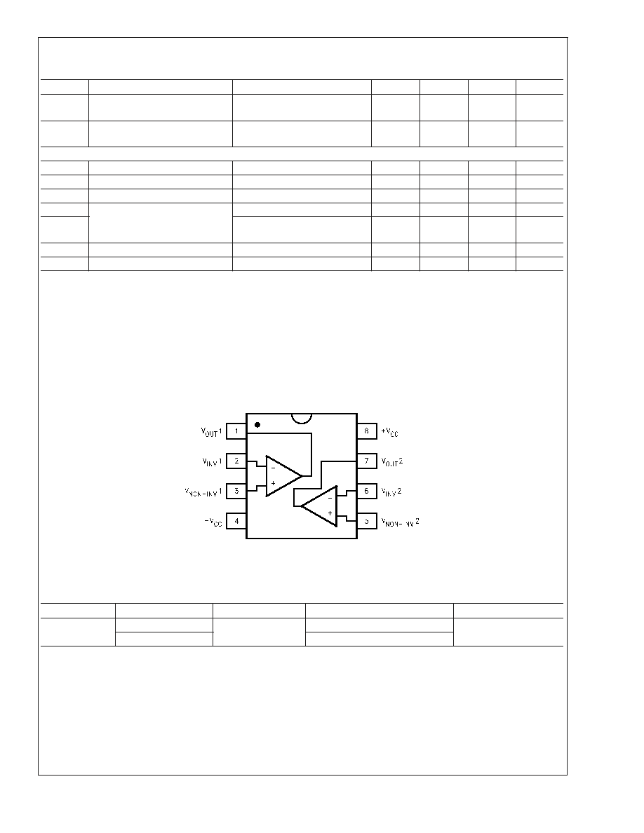
Connection Diagram
8-Pin SOIC
20042904
Top View
Ordering Information
Package
Part Number
Package Marking
Transport Media
NSC Drawing
8-pin SOIC
LMH6715MA
LMH6715MA
Rails
M08A
LMH6715MAX
2.5k Units Tape and Reel
LMH6715
www.national.com
3

Typical Performance Characteristics
(T
A
= 25∞C, V
CC
=
±
5V, A
V
=
±
2V/V, R
F
= 500
, R
L
=
100
, unless otherwise specified).
Non-Inverting Frequency Response
Inverting Frequency Response
20042913
20042912
Non-Inverting Frequency Response vs. V
OUT
Small Signal Channel Matching
20042916
20042901
Frequency Response vs. Load Resistance
Non-Inverting Frequency Response vs. R
F
20042915
20042914
LMH6715
www.national.com
4

Typical Performance Characteristics
(T
A
= 25∞C, V
CC
=
±
5V, A
V
=
±
2V/V, R
F
= 500
, R
L
= 100
,
unless otherwise specified). (Continued)
Small Signal Pulse Response
Large Signal Pulse Response
20042918
20042919
Input-Referred Crosstalk
Settling Time vs. Accuracy
20042907
20042924
-3dB Bandwidth vs. V
OUT
DC Errors vs. Temperature
20042925
20042926
LMH6715
www.national.com
5