LMH6714/6720/6722
Wideband Video Op Amp; Single, Single with Shutdown
and Quad
General Description
The
LMH6714/6720/6722
series
combine
National's
VIP10
TM
high speed complementary bipolar process with
National's current feedback topology to produce a very high
speed op amp. These amplifiers provide a 400MHz small
signal bandwidth at a gain of +2V/V and a 1800V/µs slew
rate while consuming only 5.6mA from
±
5V supplies.
The LMH6714/6720/6722 series offer exceptional video per-
formance with its 0.01% and 0.01∞ differential gain and
phase errors for NTSC and PAL video signals while driving a
back terminated 75
load. They also offer a flat gain re-
sponse of 0.1dB to 120MHz. Additionally, they can deliver
70mA continuous output current. This level of performance
makes them an ideal op amp for broadcast quality video
systems.
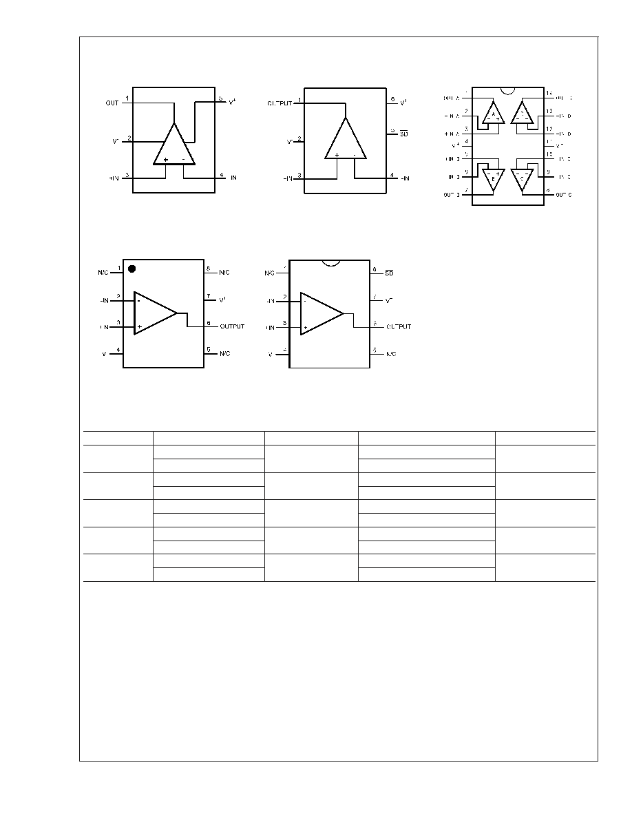
The
LMH6714/6720/6722's
small
packages
(SOIC
&
SOT23), low power requirement, low noise and distortion
allow the LMH6714/6720/6722 to serve portable RF applica-
tions. The high impedance state during shutdown makes the
LMH6720 suitable for use in multiplexing multiple high speed
signals onto a shared transmission line. The LMH6720 is
also ideal for portable applications where current draw can
be reduced with the shutdown function.
Features
n
400MHz (A
V
= +2V/V, V
OUT
= 500mV
PP
) -3dB BW
n
250MHz (A
V
= +2V/V, V
OUT
= 2V
PP
) -3dB BW
n
0.1dB gain flatness to 120MHz
n
Low power: 5.6mA
n
TTL compatible shutdown pin (LMH6720)
n
Very low diff. gain, phase: 0.01%, 0.01∞ (LMH6714)
n
-58 HD2/ -70 HD3 at 20MHz
n
Fast slew rate: 1800V/µs
n
Low shutdown current: 500uA (LMH6720)
n
11ns turn on time (LMH6720)
n
7ns shutdown time (LMH6720)
n
Unity gain stable
n
Improved replacement for CLC400,401,402,404,406 and
446 (LMH6714)
n
Improved replacement for CLC405 (LMH6720)
n
Improved replacement for CLC415 (LMH6722)
Applications
n
HDTV, NTSC & PAL video systems
n
Video switching and distribution
n
Wideband active filters
n
Cable drivers
n
High speed multiplexer (LMH6720)
n
Programmable gain amplifier (LMH6720)
Non-Inverting Small Signal Frequency Response
20056506
Differential Gain and Phase vs. Number of Video
Loads (LMH6714)
20056528
March 2003
LMH6714/6720/6722
W
ideband
V
ideo
Op
Amp;
Single,
Single
with
Shutdown
and
Quad
© 2003 National Semiconductor Corporation
DS200565
www.national.com
Absolute Maximum Ratings
(Note 1)
If Military/Aerospace specified devices are required,
please contact the National Semiconductor Sales Office/
Distributors for availability and specifications.
ESD Tolerance (Note 4)
Human Body Model
2000V
Machine Model
200V
V
CC
±
6.75V
I
OUT
(Note 3)
Common Mode Input Voltage
±
V
CC
Differential Input Voltage
2.2V
Maximum Junction Temperature
+150∞C
Storage Temperature Range
-65∞C to +150∞C
Lead Temperature (soldering 10 sec)
+300∞C
Storage Temperature Range
-65∞C to +150∞C
Shutdown Pin Voltage (Note 5)
+V
CC
to V
CC
/2-1V
Operating Ratings
(Note 3)
Thermal Resistance
Package
(
JA
)
5-Pin SOT23
232∞C/W
6-Pin SOT23
198∞C/W
8-Pin SOIC
145∞C/W
14-Pin SOIC
130∞C/W
Operating Temperature
-40∞C
+85∞C
Nominal Supply Voltage
±
5V
±
6V
Electrical Characteristics
Unless specified, A
V
= +2, R
F
= 300
: V
CC
=
±
5V, R
L
= 100
, LMH6714/6720/6722. Boldface limits apply at temperature
extremes.
Symbol
Parameter
Conditions
Min
Typ
Max
Units
Frequency Domain Response
SSBW
-3dB Bandwidth
V
OUT
= 0.5V
PP
345
400
MHz
LSBW
-3dB Bandwidth
V
OUT
= 2.0V
PP
200
250
MHz
Gain Flatness
V
OUT
= 2V
PP
GFP
Peaking
DC to 120MHz
0.1
dB
GFR
Rolloff
DC to 120MHz
0.1
dB
LPD
Linear Phase Deviation
DC to 120MHz
0.5
deg
DG
Differential Gain
R
L
= 150
, 4.43MHz
(LMH6714)
0.01
%
DG
Differential Gain
R
L
= 150
, 4.43MHz
(LMH6720)
0.02
%
DP
Differential Phase
R
L
= 150
, 4.43MHz
0.01
deg
Time Domain Response
TRS
Rise and Fall Time
.5V Step
1.5
ns
TRL
2V Step
2.6
ns
t
s
Settling Time to 0.05%
2V Step
12
ns
SR
Slew Rate
6V Step
1200
1800
V/µs
Distortion and Noise Response
HD2
2nd Harmonic Distortion
2V
PP
, 20MHz
-58
dBc
HD3
3rd Harmonic Distortion
2V
PP
, 20MHz
-70
dBc
IMD
3rd Order Intermodulation Products
10MHz, P
OUT
= 0dBm
-78
dBc
Equivalent Input Noise
VN
Non-Inverting Voltage
>
1MHz
3.4
nV/
NICN
Inverting Current
>
1MHz
10
pA/
ICN
Non-Inverting Current
>
1MHz
1.2
pA/
Static, DC Performance
V
IO
Output Offset Voltage
±
0.2
±
6
±
8
mV
DVIO
Average Drift
8
µV/∞C
I
BN
Input Bias Current
Non-Inverting
±
1
±
10
±
15
µA
DIBN
Average Drift
4
nA/∞C
LMH6714/6720/6722
www.national.com
2

Electrical Characteristics
(Continued)
Unless specified, A
V
= +2, R
F
= 300
: V
CC
=
±
5V, R
L
= 100
, LMH6714/6720/6722. Boldface limits apply at temperature
extremes.
Symbol
Parameter
Conditions
Min
Typ
Max
Units
I
BI
Input Bias Current
Inverting
-4
±
12
±
20
µA
DIBI
Average Drift
41
nA/∞C
PSRR
Power Supply Rejection Ratio
DC
48
47
58
dB
CMRR
Common Mode Rejection Ratio
DC
48
45
54
dB
I
CC
Supply Current
R
L
=
4.5
3
5.6
7.5
8
mA
I
CCI
Supply Current During Shutdown
LMH6720
500
670
µA
Miscellaneous Performance
R
IN
Input Resistance
Non-Inverting
2
M
C
IN
Input Capacitance
Non-Inverting
1.0
pF
R
OUT
Output Resistance
Closed Loop
0.06
V
O
Output Voltage Range
R
L
=
±
3.5
±
3.4
±
3.9
V
V
OL
R
L
= 100
±
3.6
±
3.4
±
3.8
V
CMIR
Input Voltage Range
Common Mode
±
2.2
V
I
O
Output Current (Note 3)
V
IN
= 0V, Max Linear Current
50
70
mA
OFFMAX
Voltage for Shutdown
LMH6720
0.8
V
ONMIN
Voltage for Turn On
LMH6720
2.0
V
IIH
Current Turn On
LMH6720, SD = 2.0V
-20
-30
2
20
30
µA
IIL
Current Shutdown
LMH6720, SD = .8V
-600
-400
-100
µA
IOZ
R
OUT
Shutdown
LMH6720, SD = .8V
0.2
1.8
M
t
on
Turn on Time
LMH6720
11
ns
t
off
Turn off Time
LMH6720
7
ns
Note 1: Absolute Maximum Ratings indicate limits beyond which damage to the device may occur. Operating Ratings indicate conditions for which the device is
intended to be functional, but specific performance is not guaranteed. For guaranteed specifications, see the Electrical Characteristics tables.
Note 2: Electrical Table values apply only for factory testing conditions at the temperature indicated. Factory testing conditions result in very limited self-heating of
the device such that T
J
= T
A
. No guarantee of parametric performance is indicated in the electrical tables under conditions of internal self heating where T
J
>
T
A
.
See Applications Section for information on temperature derating of this device." Min/Max ratings are based on product characterization and simulation. Individual
parameters are tested as noted.
Note 3: The maximum output current (I
OUT
) is determined by device power dissipation limitations. See the Power Dissipation section of the Application Division for
more details.
Note 4: Human body model, 1.5k
in series with 100pF. Machine model, 0 In series with 200pF.
Note 5: The shutdown pin is designed to work between 0 and V
CC
with split supplies (V
CC
= -V
EE
). With single supplies (V
EE
= ground) the shutdown pin should
not be taken below V
CC
/2.
LMH6714/6720/6722
www.national.com
3
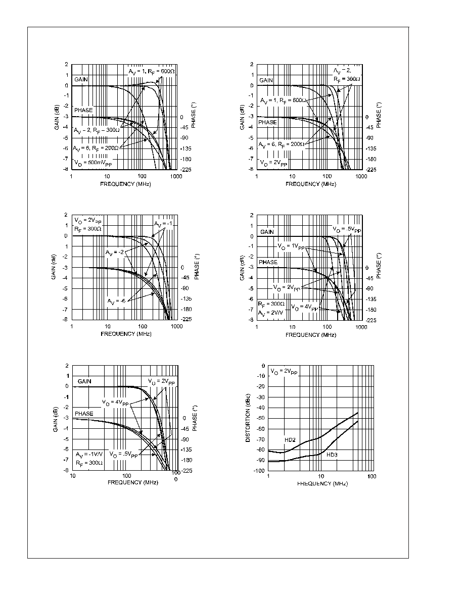
Typical Performance Characteristics
(A
V
= 2, R
F
= 300
, R
L
= 100
Unless Specified).
Non-Inverting Small Signal Frequency Response
Non-Inverting Large Signal Frequency Response
20056506
20056507
Inverting Frequency Response
Non-Inverting Frequency Response vs. V
O
20056503
20056508
Inverting Frequency Response vs. V
O
Harmonic Distortion vs. Frequency
20056509
20056504
LMH6714/6720/6722
www.national.com
5