
LMS1485
5V Low Power RS-485 Differential Bus Transceiver
General Description
The LMS1485 is a low power differential bus/line transceiver
designed for high speed bidirectional data communication on
multipoint bus transmission lines. It is designed for balanced
transmission lines. It meets ANSI Standards TIA/EIA
RS422-B, TIA/EIA RS485-A and ITU recommendation and
V.11 and X.27.
The LMS1485 combines a TRI-STATE
TM
differential line
driver and differential input receiver, both of which operate
from a single 5.0V power supply. The driver and receiver
have an active high and active low, respectively, that can be
externally connected to function as a direction control. The
driver and receiver differential inputs are internally con-
nected to form differential input/output (I/O) bus ports that
are designed to offer minimum loading to bus whenever the
driver is disabled or when V
CC
= 0V. These ports feature
wide positive and negative common mode voltage ranges,
making the device suitable for multipoint applications in
noisy environments.
The LMS1485 is build with National's advanced BiCMOS
process and is available in a 8-Pin SOIC package. It is a
drop-in socket replacement to ADI's ADM1485 and LTC's
LT1485.
Features
n
Meet ANSI standard RS-485-A and RS-422-B
n
Data rate 30Mbps
n
Single supply voltage operation, 5V
n
Wide input and output voltage range
n
Thermal shutdown protection
n
Short circuit protection
n
Driver propagation delay 10ns
n
Receiver propagation delay 25ns
n
High impedance outputs with power off
n
Open circuit fail-safe for receiver
n
Extended operating temperature range -40�C to 85�C
n
ESD rating 8kV HBM
n
Drop-in replacement to ADM1485 and LT1485
n
Available in 8-pin SOIC
n
Low supply current, I
CC
= 1mA
Applications
n
Low power RS-485 systems
n
Network hubs, bridges, and routers
n
Point of sales equipment (ATM, barcode scanners,...)
n
Local area networks (LAN)
n
Integrated service digital network (ISDN)
n
Industrial programmable logic controllers
n
High speed parallel and serial applications
n
Multipoint applications with noisy environment
Typical Application
20048801
A typical multipoint application is shown in the above figure. Terminating resistors, RT, are typically required but only located at the two ends of the cable.
Pull up and pull down resistors maybe required at the end of the bus to provide failsafe biasing. The biasing resistors provide a bias to the cable when all
drivers are in TRI-STATE, See National Application Note, AN-847 for further information.
July 2003
LMS1485
5V
Low
Power
RS-485
Differential
Bus
T
ransceiver
� 2003 National Semiconductor Corporation
DS200488
www.national.com
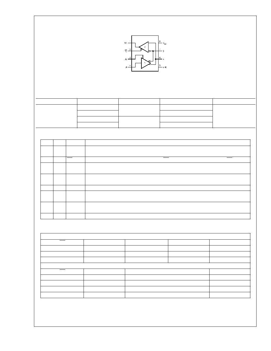
Connection Diagram
8-Pin SOIC
20048802
Top View
Ordering Information
Package
Part Number
Package Marking
Transport Media
NSC Drawing
8-Pin SOIC
LMS1485M
LMS1485M
95 Units/Rail
M08A
LMS1485MX
2.5k Units Tape and Reel
LMS1485IM
LMS1485IM
95 Units/Rail
LMS1485IMX
2.5k Units Tape and Reel
Pin Descriptions
Pin # I/O
Name
Function
1
O
RO
Receiver Output: If A
>
B by 200 mV, RO will be high; If A
<
B by 200mV, RO will be low. RO
will be high also if the inputs (A and B) are open (non-terminated)
2
I
RE
Receiver Output Enable: RO is enabled when RE is low; RO is in TRI-STATE when RE is high
3
I
DE
Driver Output Enable: The driver outputs (A and B) are enabled when DE is high; they are in
TRI-STATE when DE is low. Pins A and B also function as the receiver input pins (see below)
4
I
DI
Driver Input: A low on DI forces A low and B high while a high on DI forces A high and B low
when the driver is enabled
5
N/A
GND
Ground
6
I/O
A
Non-inverting Driver Output and Receiver Input pin. Driver Output levels conform to RS-485
signaling levels
7
I/O
B
Inverting Driver Output and Receiver Input pin. Driver Output levels conform to RS-485 signaling
levels
8
N/A
V
CC
Power Supply: 4.75V
V
CC
5.25V
Truth Table
DRIVER SECTION
RE
DE
DI
A
B
X
H
H
H
L
X
H
L
L
H
X
L
X
Z
Z
RECEIVER SECTION
RE
DE
A-B
RO
L
L
+0.2V
H
L
L
-0.2V
L
H
X
X
Z
L
L
OPEN
*
H
Note: * = Non Terminated, Open Input only
X = Irrelevant
Z = TRI-STATE
H = High level
L = Low level
LMS1485
www.national.com
2

Absolute Maximum Ratings
(Note 1)
If Military/Aerospace specified devices are required,
please contact the National Semiconductor Sales Office/
Distributors for availability and specifications.
Supply Voltage, V
CC
(Note 2)
7V
Input Voltage, V
IN
(DI, DE, or RE)
-0.3V to V
CC
+ 0.3V
Voltage Range at Any Bus Terminal
(AB)
-7V to 12V
Receiver Outputs
-0.3V to V
CC
+ 0.3V
Package Thermal Impedance,
JA
SOIC (Note 3)
125�C/W
Junction Temperature (Note 3)
150�C
Operating Free-Air Temperature
Range, T
A
Commercial
0�C to 70�C
Industrial
-40�C to 85�C
Storage Temperature Range
-65�C to 150�C
ESD Rating (Note 4) (Note 8)
8kV
ESD Rating (Note 4) (Note 9)
2kV
Soldering Information
Infrared or Convection (20 sec.)
235�C
Operating Ratings
Min Nom Max
Supply Voltage, V
CC
4.75
5.0
5.25
V
Voltage at any Bus Terminal
(Separately or Common Mode)
-7
12
V
V
IN
or V
IC
High-Level Input Voltage, V
IH
(Note 5)
2
V
Low-Level Input Voltage, V
IL
(Note 5)
0.8
V
Differential Input Voltage, V
ID
(Note 6)
�
12
V
Electrical Characteristics
Over recommended ranges of supply voltage and operating free-air temperature (unless otherwise noted)
Symbol
Parameter
Conditions
Min
Typ
Max
Units
Driver Section
V
OD
Differential Output Voltage
R =
(Figure 1)
5
V
V
OD1
Differential Output Voltage
R = 50
(Figure 1), RS-422
2
5
V
V
OD2
Differential Output Voltage
R = 27
(Figure 1), RS-485
1.5
5
V
V
OD3
Differential Output Voltage
V
TEST
= -7V to + 12V (Figure 2)
1.5
5
V
V
OD
Change in Magnitude of
Differential Output Voltage
R = 27
or 50 (Figure 1 ), (Note 7)
-0.2
0.2
V
V
OC
Common-Mode Output
Voltage
R = 27
or 50 (Figure 1), (Note 7)
3
V
V
OC
Change in Magnitude of
Common-Mode Output
Voltage
R = 27
or 50 (Figure 1), (Note 7)
-0.2
0.2
V
I
OSD
Short-Circuit Output Current
V
O
= High, -7V
V
CM
+12V
-250
250
mA
V
O
= Low, -7V
V
CM
+12V
-250
250
V
INL
CMOS Input Logic Threshold
Low
DE, DI, RE
0.8
V
V
INH
CMOS Input Logic Threshold
High
DE, DI, RE
2
V
I
IN
Logic Input Current
DE, DI
-1
1
�A
Receiver Section
V
TH
Differential Input Threshold
Voltage
-7V
V
CM
+ 12V
-0.2
+0.2
V
V
TH
Input Hysteresis Voltage
(V
TH+
- V
TH-
)
V
CM
= 0
70
mV
R
IN
Input Resistance
-7V
V
CM
+ 12V
12
k
I
IN
Input Current (A, B)
V
IN
= 12V
1
mA
V
IN
= -7V
-0.8
I
RE
Logic Enable Input Current
RE
-1
1
�A
V
OL
CMOS Low-Level Output
Voltage
I
OL
= 4mA
0.4
V
LMS1485
www.national.com
3

Electrical Characteristics
(Continued)
Over recommended ranges of supply voltage and operating free-air temperature (unless otherwise noted)
Symbol
Parameter
Conditions
Min
Typ
Max
Units
V
OH
CMOS High-Level Output
Voltage
I
OH
= -4mA
4
V
I
OSR
Short-Circuit Output Current
V
O
= GND or V
CC
7
85
mA
I
OZ
Tristate Output Leakage
Current
0.4V
V
O
+2.4V
-1
1
�A
Power Supply Current
I
CC
Supply Current
Driver Enabled, Output = No Load,
Digital Inputs = GND or V
CC
1.1
2.2
mA
Driver Disabled, Output = No Load,
Digital Inputs = GND or V
CC
1
2.2
mA
Switching Characteristics
Driver
T
PLH
,
T
PHL
Propagation Delay Input to
Output
R
L
= 54
, C
L
= 100pF
(Figure 3, Figure 7)
11
20
ns
T
SKEW
Driver Output Skew
R
L
= 54
, C
L
= 100pF
(Figure 3, Figure 7)
1
ns
T
R
,
T
F
Driver Rise and Fall Time
R
L
= 100
, C
L
= 100pF
(Figure 3, Figure 7)
5
10
ns
T
ENABLE
Driver Enable to Ouput Valid
Time
(Figure 4, Figure 8)
18
32
ns
T
DISABLE
Output Disable Time
(Figure 4, Figure 8)
20
40
ns
Receiver
T
PLH
,
T
PHL
Propagation Delay Input to
Output
C
L
= 15pF
(Figure 5, Figure 7)
18
33
55
ns
T
SKEW
Receiver Output Skew
(Figure 5, Figure 7)
2
ns
T
ENABLE
Receiver Enable Time
(Figure 6, Figure 10)
6
25
ns
T
DISABLE
Receiver Disable Time
(Figure 6, Figure 10)
15
25
ns
Note 1: Absolute Maximum Ratings indicate limits beyond which damage to the device may occur. Operating Ratings indicate conditions for which the device is
intended to be functional, but specific performance is not guaranteed. For guaranteed specifications and the test conditions, see the Electrical Characteristics
Note 2: All voltage values, except differential I/O bus voltage, are with respect to network ground terminal.
Note 3: The maximum power dissipation is a function of T
J(MAX)
,
JA
, and T
A
. The maximum allowable power dissipation at any ambient temperature is P
D
=
(T
J(MAX)
- T
A
)/
JA
. All numbers apply for packages soldered directly into a PC board.
Note 4: ESD rating based upon human body model, 100pF discharged through 1.5k
.
Note 5: Voltage limits apply to DI, DE, RE pins.
Note 6: Differential input/output bus voltage is measured at the non-inverting terminal A with respect to the inverting terminal B.
Note 7: |
V
OD
| and |
V
OC
| are changes in magnitude of V
OD
and V
OC
, respectively when the input changes from high to low levels.
Note 8: ESD rating applies to pins 6 and 7
Note 9: ESD rating applies to pins 1, 2, 3, 4, 5 and 8
LMS1485
www.national.com
4
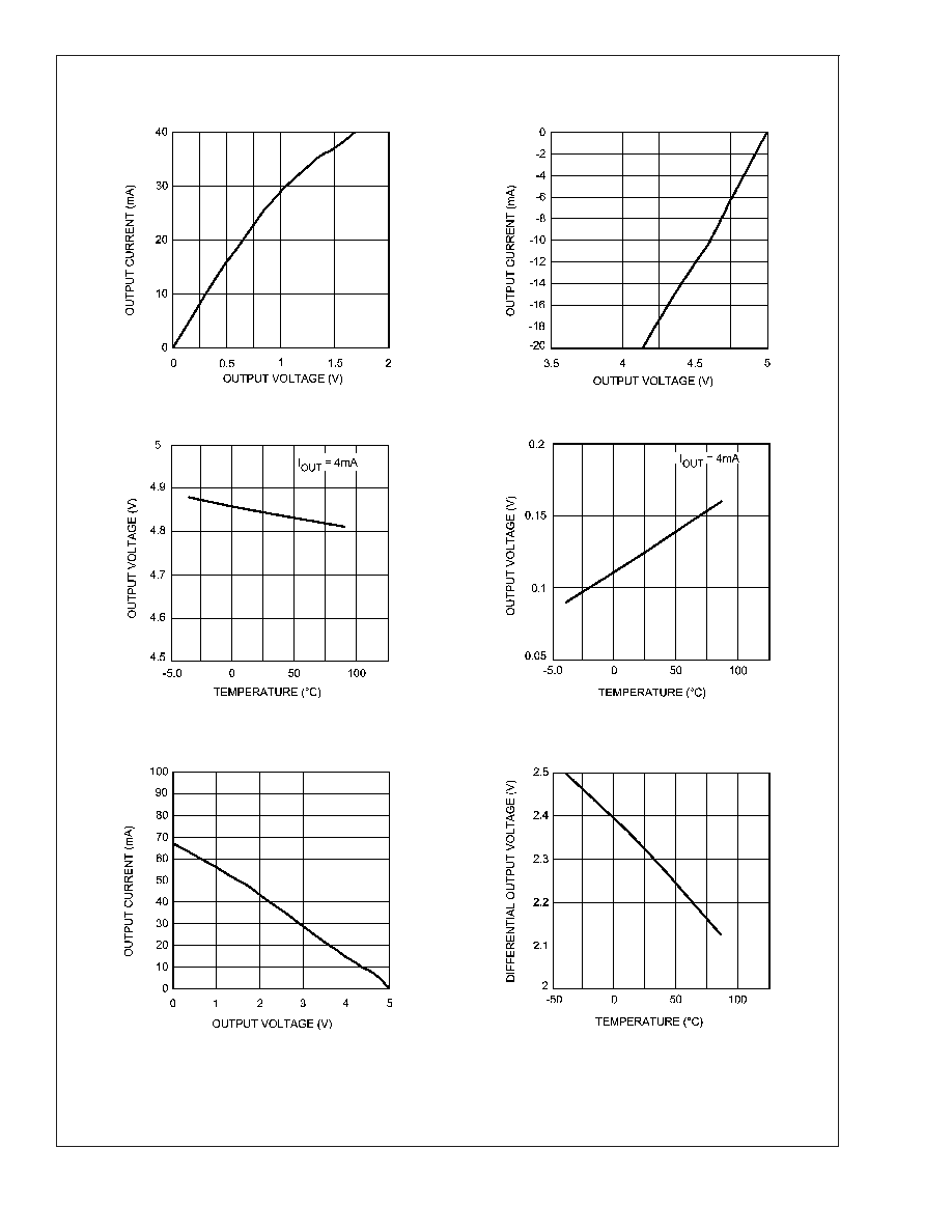
Typical Performance Characteristics
Receiver Output Low Voltage vs. Output Current
Receiver Output High Voltage vs. Output Current
20048813
20048814
Receiver Output High Voltage vs. Temperature
Receiver Output Low Voltage vs. Temperature
20048815
20048816
Driver Differential Output Voltage vs. Output Current
Driver Differential Output Voltage vs. Temperature
R
L
= 54
20048817
20048818
LMS1485
www.national.com
5