 | –≠–ª–µ–∫—Ç—Ä–æ–Ω–Ω—ã–π –∫–æ–º–ø–æ–Ω–µ–Ω—Ç: LMS202 | –°–∫–∞—á–∞—Ç—å:  PDF PDF  ZIP ZIP |
LMS202
5V Single Supply TIA/EIA-232 Dual Transceivers
General Description
The LMS202 features two transmitters and two receivers for
RS-232 communication. It has a DC-to-DC converter that
permits the device to operate with only a single +5V power
supply. The on-chip DC-to-DC converter which utilizes four
external 0.1µF capacitors to generate dual internal power
supplies for RS-232 compatible output levels.
The device meet EIA/TIA-232E and CCITT V.28 specifica-
tions up to 230kbits/sec. The LMS202 is available in a 16 pin
narrow and Wide SOIC package.
Features
n
Single +5V power supply
n
230 kbps data rate
n
On-board DC-to-DC converter
n
0.1µF charge pump capacitors
n
Drop-in replacement to Maxim's MAX202
Applications
n
POS equipment (Bar code reader)
n
Hand-held equipment
n
General purpose RS-232 communication
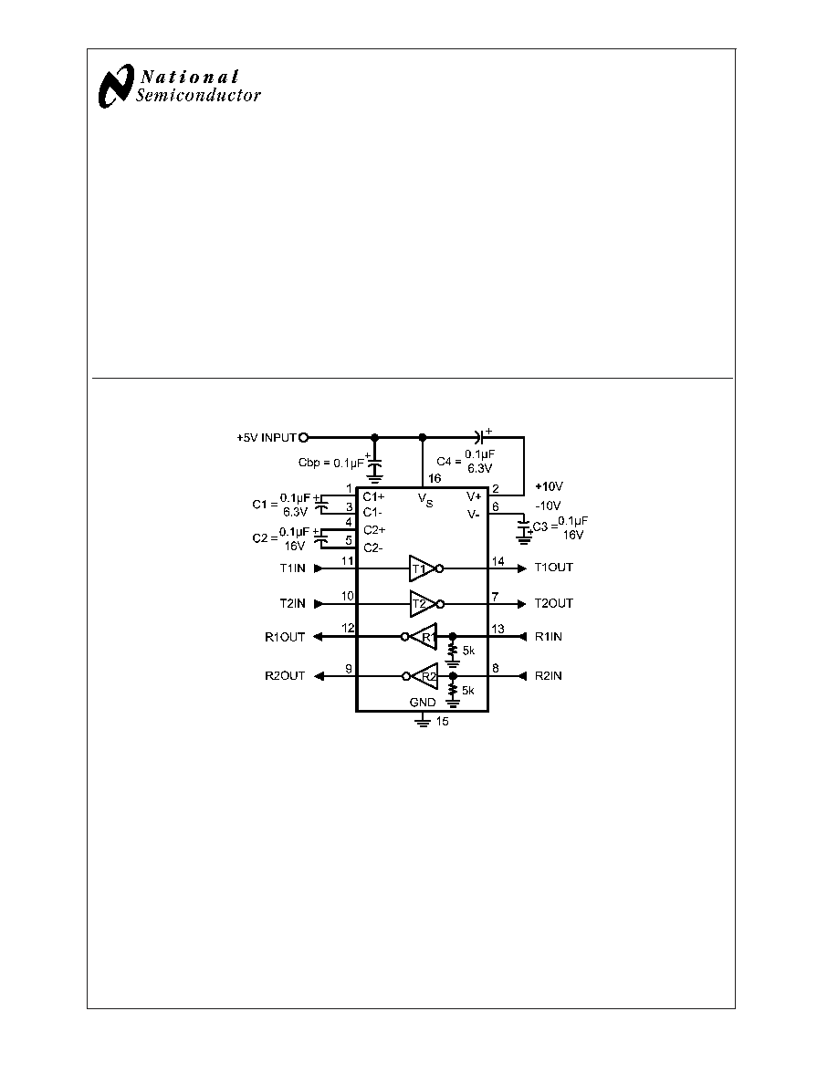
Connection Diagram and Typical Circuit
20062901
March 2003
LMS202
5V
Single
Supply
TIA/EIA-232
Dual
T
ransceivers
© 2003 National Semiconductor Corporation
DS200629
www.national.com
Pin Descriptions
Pin Number
Pin Name
Pin Function
1, 3
C1+, C1-
External capacitor connection pins. Recommended external capacitor C1 = 0.1µF (6.3V)
2
V+
Positive supply for TIA/EIA-232E drivers. Recommended external capacitor C4 = 0.1µF (6.3V)
4, 5
C2+, C2-
External capacitor connection pins. Recommended external capacitor C2 = 0.1µF (16V)
6
V-
Negative supply for TIA/EIA-232E drivers. Recommended external capacitor C3 = 0.1µF (16V)
7, 14
T1out, T2out
Transmitter output pins conform to TIA/EIA-232E levels. The typical transmitter output swing is
±
8V when loaded 3k
load to ground. The open-circuit output voltage swings from (V+ - 0.6V)
to V-
8,13
R1in, R2in
Receiver inputs accept TIA/EIA-232
9, 12
R1out and R2out Receiver output pins are TTL/CMOS compatible
10, 11
Tin1, Tin2
Transmitter input pins are TTL/CMOS compatible. Inputs of transmitter do not have pull-up
resistors. Connect all unused transmitter inputs to ground
15
GND
Ground pin
16
V
S
Power supply pin for the device, +5V (
±
10%)
Ordering Information
Package
Part Number
Package Marking
Transport Media
NSC Drawing
16-Pin SOIC
LMS202CM
LMS202CM
48 Units/Rail
M16A
LMS202CMX
2.5k Units Tape and Reel
LMS202IM
LMS202IM
48 Units/Rail
LMS202IMX
2.5k Units Tape and Reel
16-Pin Wide SOIC
LMS202CMW
LMS202CMW
45 Units/Rail
M16B
LMS202CMWX
1.0k Units Tape and Reel
LMS202IMW
LMS202IMW
45 Units/Rail
LMS202IMWX
1.0k Units Tape and Reel
LMS202
www.national.com
2
Absolute Maximum Ratings
(Note 1)
If Military/Aerospace specified devices are required,
please contact the National Semiconductor Sales Office/
Distributors for availability and specifications.
V
S
-0.3V to 6V
V+
(V
S
- 0.3V) to + 14V
V-
+0.3V to -14V
Driver Input Voltage, T
IN
-0.3V to (V+ +0.3V)
Receiver Input Voltage, R
IN
±
30V
Driver Output Voltage T
O
(V- -0.3V to (V+ + 0.3V)
Receiver Output Voltage R
O
-0.3 to (V
S
+ 0.3)
Short Circuit Duration, T
O
Continuous
ESD Rating
Human Body Model (Note 2)
2kV
Machine Model (Note 6)
200V
Soldering Information
Infrared or Convection
235∞C
(20sec.)
Junction Temperature
150∞C
Storage Temperature Range
-65∞C to +150∞C
Operating Ratings
Supply Voltage V
S
4.5V to 5.5V
Ambient Temperature Range, T
A
Commercial (C)
0∞C to +70∞C
Industrial (I)
-40∞C to +85∞C
Package Thermal Resistance
(Note 3)
SO
71∞C/W
WSO
55∞C/W
Electrical Characteristics
Over recommended operating supply and temperature ranges unless otherwise specified C1 = C2 = C3 = C4 = Cbp = 0.1µF
Symbol
Parameter
Conditions
Min
(Note 5)
Typ
Max
(Note 5)
Units
DC Characteristics
I
S
Supply Current
No Load, T
A
= 25∞C
1
7
mA
Logic
I
INPUT
Input Leakage Current
T
IN
= 0V to V
S
±
10
µA
V
THL
Input Logic Theshold Low
T
IN
0.8
V
V
THH
Input Logic Theshold High
T
IN
2.0
V
V
OL
TTL/CMOS Output Voltage
Low
R
OUT
, I
OUT
= 3.2mA
0.4
V
V
OH
TTL/CMOS Output Voltage
High
R
OUT
, I
OUT
= -1.0mA
3.5
V
S
-0.1
V
RS-232 Receiver Inputs
V
RI
Receiver Input Voltage
Range
-30
+30
V
V
RTHL
Receiver Input Theshold
Low
V
S
= 5V, T
A
= 25∞C
0.8
1.4
V
V
RTHH
Receiver Input Theshold
High
V
S
= 5V, T
A
= 25∞C
2
2.4
V
V
HYST
Receiver Input Hysteresis
V
S
= 5V
0.2
0.6
1.0
V
R
I
Receiver Input Resistance
V
S
= 5V, T
A
= 25∞C
3
5
7
k
RS-232 Transmitter Outputs
V
O
Transmitter Output Voltage
Swing
All transmitters loaded with 3k
to GND
±
5
±
8
V
R
O
Output Resistance
V
S
= V+ = V- = 0V,
V
O
=
±
2V
300
I
OS
Output Short Circuit Current
±
11
±
60
mA
Timing Characteristics
DR
Maximum Data Rate
C
L
= 50pF to 1000pF,
R
L
= 3k
to 7k
230
kbps
T
RPLH
T
RPHL
Receiver Propagation Delay C
L
= 150pF
0.08
1
µs
T
DPLH
T
DPHL
Transmitter Propagation
Delay
R
L
= 3k
, C
L
= 2500pF
All transmitters loaded
2.4
µs
LMS202
www.national.com
3

Electrical Characteristics
(Continued)
Over recommended operating supply and temperature ranges unless otherwise specified C1 = C2 = C3 = C4 = Cbp = 0.1µF
Symbol
Parameter
Conditions
Min
(Note 5)
Typ
Max
(Note 5)
Units
V
SLEW
Transition Region Slew Rate T
A
= 25∞C, V
S
= 5V
C
L
= 50pF to 1000pF, R
L
= 3k
to 7k
Measured from +3V to -3V or vice versa
3
6
30
V/µs
Note 1: Absolute Maximum Ratings indicate limits beyond which damage to the device may occur. Operating Ratings indicate conditions for which the device is
intended to be functional, but specific performance is not guaranteed. For guaranteed specifications and the test conditions, see the Electrical Characteristics.
Note 2: Human Body Model, 1.5k
in series with 100pF
Note 3: The maximum power dissipation is a function of T
J(MAX),
JA,
and T
A.
The maximum allowable power dissipation at any ambient temperature is P
D
=
(T
J(MAX)
- T
A
)/
JA.
All numbers apply for packages soldered directly onto a PC board.
Note 4: Typical Values represent the most likely parametric norm.
Note 5: All limits are guaranteed by testing or statistical analysis
Note 6: Machine model, 0
in series with 200pF
Typical Characteristics
Transmitter Output High Voltage vs. Load Capacitance
Transmitter Slew Rate vs. Load Capacitance
20062902
20062903
Application Information
CAPACITOR SELECTION
The recommended capacitors are 0.1µF. However, larger
capacitors for the charge pump may be used to minimized
ripples on V+ and V- pins.
POWER SUPPLY DECOUPLING
In some applications that are sensitive to power supply noise
from the charge pump, place a decoupling capacitor, Cbp,
from V
S
to GND. Use at least a 0.1µF capacitor or the same
size as the charge pump capacitors (C1 - C4).
CHARGED PUMP
The dual internal charged-pump provides the
±
10V to the to
transmitters. Using capacitor C1, the charge pump converts
+5V to +10V then stores the +10V in capacitor C3. The
charge pump uses capacitor C2 to invert the +10V to -10V.
The -10V is then stored in capacitor C4.
LMS202
www.national.com
4

Physical Dimensions
inches (millimeters) unless otherwise noted
16-Pin SOIC
NS Package Number M16A
16-Pin Wide SOIC
NS Package Number M16B
LMS202
www.national.com
5