
LMS5213
80mA, µCap, Low Dropout Voltage Regulator in SC70
General Description
∑
The LMS5213 is a µCap, low dropout voltage regulator
with very low quiescent current, 220µA typical, at 80mA
load. It also has very low dropout voltage, typically 20mV
at light load and 330mV at 80mA.
The LMS5213 provides up to 80mA and consumes a typical
of 1µA in disable mode.
The LMS5213 is optimized to work with low value, low cost
ceramic capacitors. The output typically require only 0.47µF
of output capacitance for stability. The enable pin can be tied
to V
IN
for easy device layout.
The LMS5213 is designed for portable, battery powered
equipment applications with small space requirements.
The LMS5213 is available in a space saving 5-pin SC70
package. Performance is specified for the -40∞C to +125∞C
temperature range and is available in 2.8V, 3.0V and 3.3V
fixed voltages. For other output voltage options, please con-
tact National Semiconductor.
Features
n
Space saving SC70 package
n
Available in 2.8V, 3.0V, and 3.3V fixed voltages
n
Guaranteed 80mA output
n
Low quiescent current
n
Low dropout voltage
n
Low temperature coefficient
n
Current and thermal limiting
n
Logic-controlled shutdown
n
Stability with low-ESR ceramic capacitors
n
Pin-to-pin replacement for Mic
TM
5213
Applications
n
Cellular Phones
n
Battery-powered equipment
n
Bar code scanner
n
Laptop/palmtop computer
n
High-efficiency linear power supplies
Typical Application
20010919
January 2004
LMS5213
80mA,
µCap,
Low
Dropout
V
oltage
Regulator
in
SC70
© 2004 National Semiconductor Corporation
DS200109
www.national.com

Absolute Maximum Ratings
(Note 1)
If Military/Aerospace specified devices are required,
please contact the National Semiconductor Sales Office/
Distributors for availability and specifications.
ESD Tolerance (Note 2)
Human Body Model
2000V
Junction Temperature
150∞C
V
IN
, V
OUT
, V
EN
-0.3 TO 6.5V
Soldering Information
Infrared or Convection (20 sec)
235∞C
Wave Soldering (10 sec)
260∞C (lead temp)
Operating Ratings
Supply Voltages
V
IN
2.7V to 6V
V
EN
0V to V
IN
Junction Temp. Range (Note 3)
-40∞C to +125∞C
Storage Temperature Range
-65∞C to 150∞C
Package Thermal Resistance
SC70-5
478∞C/W
Electrical Characteristics
Unless otherwise specified, all limits guaranteed for T
J
= 25∞C, V
IN
= V
OUT
+ 1V, I
L
= 1mA, C
L
= 0.47µF, V
EN
2.0V. Boldface
limits apply at the temperature extremes.
Symbol
Parameter
Conditions
Min
(Note 5)
Typ
(Note 4)
Max
(Note 5)
Units
V
O
Output Voltage Accuracy
-3
-4
3
4
%
V
O
/
T
Output Voltage Temp.
Coefficient
(Note 10)
50
200
ppm/∞C
V
O
/V
O
Line Regulation
V
IN
= V
OUT
+1V to 6V
0.008
0.3
0.5
%
V
O
/V
O
Load Regulation
I
L
= 0.1mA to 80mA (Note 6)
0.08
0.3
0.5
%
V
IN
-V
O
Dropout Voltage
(Note 7)
I
L
= 100µA
20
mV
I
L
= 20mA
70
350
I
L
= 50mA
180
I
L
= 80mA
330
600
I
Q
Quiescent Current
V
EN
0.4V (Shutdown)
1
10
µA
I
GND
Ground Pin Current
I
L
= 100µA, V
EN
2.0V (active)
160
µA
I
L
= 20mA, V
EN
2.0V (active)
180
750
I
L
= 50mA, V
EN
2.0V (active)
200
I
L
= 80mA, V
EN
2.0V (active)
220
3000
I
GNDDO
Ground Pin Current at
Dropout, (Note 8)
V
IN
= V
OUT(NOMINAL)
≠0.5V
200
300
µA
I
LIMIT
Current Limit
V
OUT
= 0V
180
250
mA
V
O
/
P
D
Thermal Regulation
(Note 9)
0.05
%W
Enable Input
V
IL
Enable Input Voltage Level
Logic Low (off)
0.6
V
V
IH
Logic High (on)
2.0
V
I
IL
Enable Input Current
V
IL
0.6V
0.01
1
µA
I
IH
V
IH
2.0V
15
50
µA
Note 1: Absolute Maximum Ratings indicate limits beyond which damage to the device may occur. Operating Ratings indicate conditions for which the device is
intended to be functional, but specific performance is not guaranteed. For guaranteed specifications and the test conditions, see the Electrical Characteristics.
Note 2: Human body model, 1.5k
in series with 100pF.
Note 3: The maximum power dissipation is a function of T
J(max)
,
JA
, and T
A
. The maximum allowable power dissipation at any ambient temperature
is P
D
= (T
J(max)
≠T
A
)/
JA
. All numbers apply for packages soldered directly into a PC board.
Note 4: Typical Values represent the most likely parametric norm.
Note 5: All limits are guaranteed by testing or statistical analysis.
Note 6: Regulation is measured at constant junction temperature using low duty cycle pulse testing. Changes in output voltage due to heating effects are covered
by the thermal regulation specification.
Note 7: Dropout voltage is defined as the input to output differential at which the output voltage drops 2% below its nominal value measured at 1V differential.
Note 8: Ground pin current is the regulator quiescent current plus pass transistor base current. The total current drawn from the supply is the sum of the load current
plus the ground pin current.
LMS5213
www.national.com
4
Electrical Characteristics
(Continued)
Note 9: Thermal regulation is defined as the change in output voltage at a time "t" after a change in power dissipation is applied, excluding load or line regulation
effects. Specifications are for an 80mA load pulse at V
IN
= 6V for t = 16ms.
Note 10: Output voltage temperature coefficient is defined as the worst-case voltage change divided by the total temperature range.
Typical Characteristics
Unless otherwise
specified, T
A
= 25∞C, V
OUT
= 2.8V, C
L
= 0.47µF
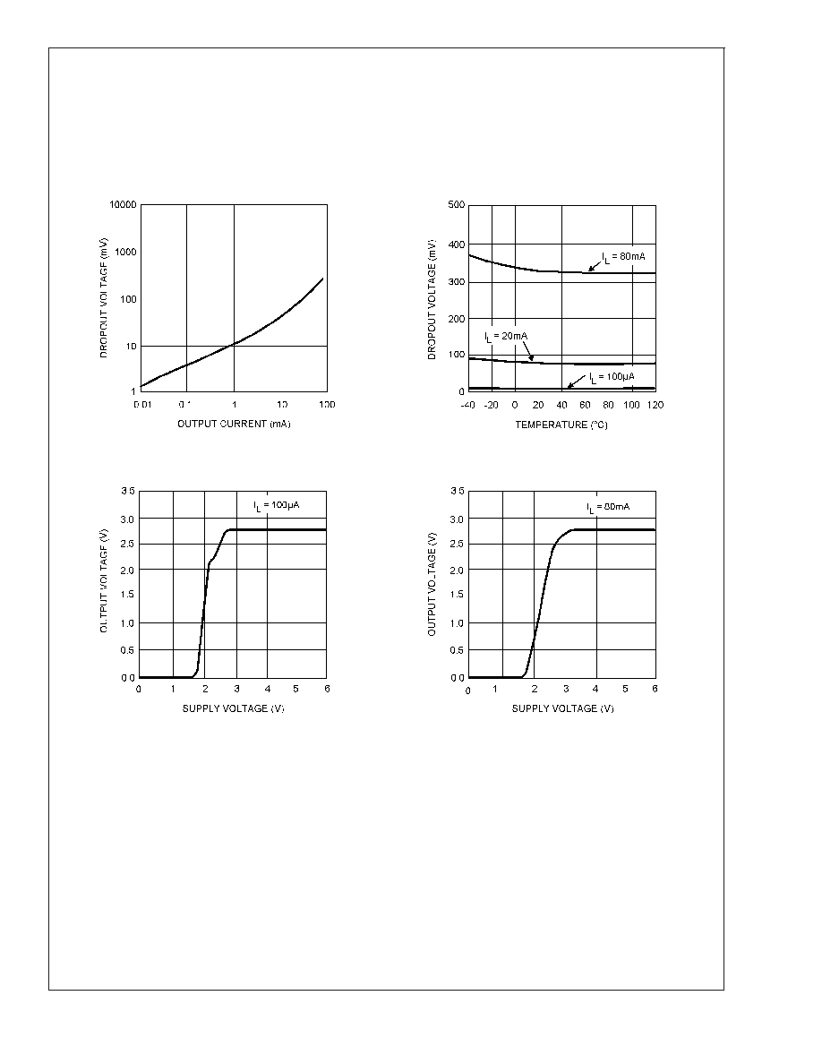
Dropout Voltage vs. Output Current
Dropout Voltage vs. Temperature
20010912
20010901
Dropout Characteristics
Dropout Characteristics
20010906
20010907
LMS5213
www.national.com
5

