LP2967
Dual Micropower 150 mA Low-Dropout Regulator in
micro SMD Package
General Description
The LP2967 is a 150 mA, dual fixed-output voltage regulator
designed to provide ultra low-dropout and low noise in bat-
tery powered applications.
Using an optimized VIP (Vertically Integrated PNP) process,
the LP2967 delivers unequalled performance in all specifi-
cations critical to battery powered designs:
Dropout Voltage: Typically 240 mV at 150 mA load, and
6 mV at 1 mA load for each output.
Ground Pin Current: Typically 1 mA at 150 mA load, and
200 µA at 1 mA load for each output.
Enhanced Stability: The LP2967 is stable with output ca-
pacitor ESR as low as 5 m
, which allows the use of ceramic
capacitors on the output.
Sleep Mode: Less than 2 µA quiescent current when SD
pins are pulled low.
Smallest Possible Size: micro SMD package uses absolute
minimum board space.
Precision Output: 1.25% tolerance.
Low Noise: By adding a 100 nF bypass capacitor, output
noise can be reduced to 30 µV (typical).
Multiple voltage options, from 1.8V to 5.0V, are available.
Consult factory for custom voltages.
Features
n
Ultra low drop-out voltage
n
Guaranteed 150mA output current, 300 mA peak
n
Smallest possible size (micro SMD package)
n
Requires minimum external components
n
Stable with 2.2 µF tantalum or ceramic capacitor
n
Output voltage accuracy
±
1%
n
<
2 µA quiescent current when shut down
n
Wide supply voltage range (16V max.)
n
Low Z
OUT
: 0.3
typical (10 Hz to 1 MHz)
n
Over temperature/over current protection
n
-40∞C to +125∞C junction temperature range
n
Custom voltages available
Applications
n
Cellular Phone
n
Palmtop/Laptop Computer
n
Personal Digital Assistance (PDA)
n
Camcorder, Personal Stereo and Camera
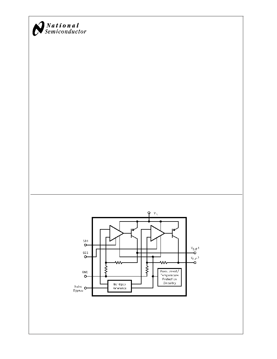
Block Diagram
10114201
April 2003
LP2967
Dual
Micropower
150
mA
Low-Dropout
Regulator
in
micro
SMD
Package
© 2003 National Semiconductor Corporation
DS101142
www.national.com
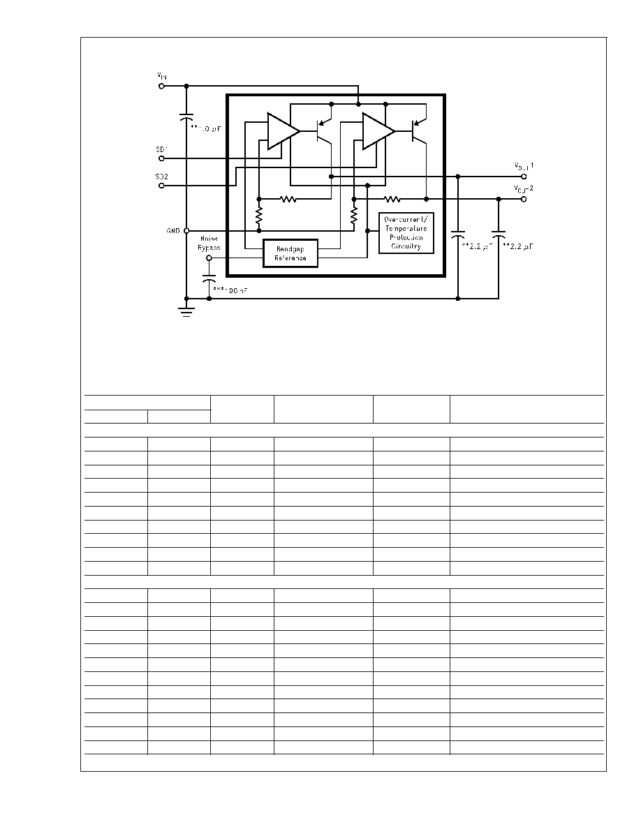
Basic Application Circuit
10114202
*SD1 and SD2 must be actively terminated. Tie them to V
IN
if their functions are not needed.
**Minimum capacitance are shown to ensure stability (may be increased without limit).
*** Reduces output noise (may be omitted if application is not noise critical). Use ceramic or film type with very low leakage current.
Ordering Information
Output Voltage (V)
Grade
Order Information
Package
Marking
Supplied As
V
OUT1
V
OUT2
For MSOP Package
2.5
2.8
STD
LP2967IMM-2528
LCAB
1000 Units Tape and Reel
2.5
2.8
STD
LP2967IMMX-2528
LCAB
3000 Units Tape and Reel
2.5
3.3
STD
LP2967IMM-2533
LCBB
1000 Units Tape and Reel
2.5
3.3
STD
LP2967IMMX-2533
LCBB
3000 Units Tape and Reel
2.6
2.6
STD
LP2967IMM-2626
LCLB
1000 Units Tape and Reel
2.6
2.6
STD
LP2967IMMX-2626
LCLB
3000 Units Tape and Reel
2.8
2.8
STD
LP2967IMM-2828
LAQB
1000 Units Tape and Reel
2.8
2.8
STD
LP2967IMMX-2828
LAQB
3000 Units Tape and Reel
2.8
3.3
STD
LP2967IMM-2833
LCCB
1000 Units Tape and Reel
2.8
3.3
STD
LP2967IMMX-2833
LCCB
3000 Units Tape and Reel
For 8-Bump micro SMD Package (BPA08)
1.8
2.5
STD
LP2967IBP-1825
L0P
1000 Units Tape and Reel
1.8
2.5
STD
LP2967IBPX-1825
L0P
3500 Units Tape and Reel
1.8
3.3
STD
LP2967IBP-1833
L0R
1000 Units Tape and Reel
1.8
3.3
STD
LP2967IBPX-1833
L0R
3500 Units Tape and Reel
2.5
2.8
STD
LP2967IBP-2528
CA
1000 Units Tape and Reel
2.5
2.8
STD
LP2967IBPX-2528
CA
3500 Units Tape and Reel
2.5
3.3
STD
LP2967IBP-2533
CB
1000 Units Tape and Reel
2.5
3.3
STD
LP2967IBPX-2533
CB
3500 Units Tape and Reel
2.6
2.6
STD
LP2967IBP-2626
CL
1000 Units Tape and Reel
2.6
2.6
STD
LP2967IBPX-2626
CL
3500 Units Tape and Reel
2.8
2.8
STD
LP2967IBP-2828
AQ
1000 Units Tape and Reel
2.8
2.8
STD
LP2967IBPX-2828
AQ
3500 Units Tape and Reel
LP2967
www.national.com
2

Package Outline and Connection Diagram
10114203
Top View
micro SMD
8-Bump micro SMD Package
Code: BP
10114204
Top View
Mini SO-8 Package
8-Lead Small Outline Integrated Circuit (SOIC) Package
Code: MM
Pin Description
Name
Pin Number
Function
micro SMD
MSOP
V
OUT
2
A1
7
Output voltage of the second LDO
SD2
B1
6
Shutdown input for the second LDO
BYPASS
C1
5
Bypass capacitor for the bandgap
GND
C2
-
Ground Substrate
GND
C3
4
Common Ground
SD1
B3
3
Shutdown input for the first LDO
V
OUT
1
A3
2
Output voltage of the first LDO
V
IN
A2
1, 8
Common input voltage for both LDOs
LP2967
www.national.com
4

Absolute Maximum Ratings
(Note 1)
If Military/Aerospace specified devices are required,
please contact the National Semiconductor Sales Office/
Distributors for availability and specifications.
Storage Temperature Range
-65∞C to +150∞C
Lead Temp. ( IR reflow, 10 sec.)
245∞C
Pad Temp. (IR reflow, 10 sec.)
245∞C
Operating Junction Temp. Range
-40∞C to +125∞C
Power Dissipation (Note 4)
Internally Limited
ESD Rating (Note 2)
1.5kV
Input Supply Voltage (Survival)
-0.3V to +16V
Input Supply Voltage (Operating)
2.1V to +16V
Shutdown Input Voltage (Survival)
-0.3V to +16V
Output Voltage (Survival) (Note 4)
I
OUT
(Survival)
Short Circuit Protected
Input-Output Voltage (Survival),
(Note 5)
-0.3V to + 16V
Electrical Characteristics
Limits in standard typeface are for T
j
= 25∞C, and limits in boldface type apply over the full operating junction temperature
range. Unless otherwise specified, V
IN
= V
O(NOM)
+ 1V, I
L
= 1mA, C
IN
= 1µF,C
OUT
= 4.7µF, V
ON/OFF
= 1.6V.
Symbol
Parameter
Conditions
Min
Typ
Max
Units
Operating Specifications
V
O
Output Voltage
Tolerance
I
LOAD
= 1mA
1mA
<
I
LOAD
<
150 mA
-1.25
-3.0
1.25
3.0
%
V
O
/
V
IN
Line Regulation
V
O
(NOM) + 1V
<
V
IN
<
16V
0.08
%/V
V
O
/
I
LOAD
Load Regulation
V
IN
= V
O(NOM)
+ 1V (Note 6)
1mA
<
I
LOAD
<
150 mA
-5
mV/V
(V
IN
- V
O
) Min.
Dropout Voltage
(Note 7)
I
LOAD
= 1mA
6
10
15
mV
I
LOAD
= 50mA
100
125
180
I
LOAD
= 150mA
240
290
425
Operating Currents
I
Q
Quiescent Current
Both Regulators ON
I
LOAD
(1 and 2) = 1mA
200
300
µA
I
LOAD
(1 and 2) = 150mA
1700
5000
One Regulator OFF
I
LOAD
(1 and 2) = 1mA
180
250
I
LOAD
(1 and 2) = 150mA
1000
2500
Both Regulators OFF
(Shutdown)
2
I
PEAK
Peak Output
Current
V
O
<
V
OUT
(NOM) - 5%
200
450
mA
Control Inputs (SD1, SD2)
V
IN
(H)
Regulator ON
Control Input
Voltage
1.6
1.4
V
V
IN
(L)
Regulator OFF
Control Input
Voltage
V
O
<
V
OUT
(NOM) - 5%
0.300
0.8
V
I
ON/OFF
Control Input
Current
V
(SD)
= 0V
V
(SD)
= 5V
-2
7
µA
Dynamic Characteristics
e
n
Output Noise
Voltage
C
BYPASS
= 100nF, 300 to
100kHz
30
µV rms
LP2967
www.national.com
5
