 | –≠–ª–µ–∫—Ç—Ä–æ–Ω–Ω—ã–π –∫–æ–º–ø–æ–Ω–µ–Ω—Ç: MAX660M | –°–∫–∞—á–∞—Ç—å:  PDF PDF  ZIP ZIP |
MAX660
Switched Capacitor Voltage Converter
General Description
The MAX660 CMOS charge-pump voltage converter inverts
a positive voltage in the range of 1.5V to 5.5V to the corre-
sponding negative voltage. The MAX660 uses two low cost
capacitors to provide 100 mA of output current without the
cost, size, and EMI related to inductor based converters.
With an operating current of only 120 µA and operating effi-
ciency greater than 90% at most loads, the MAX660 pro-
vides ideal performance for battery powered systems. The
MAX660 may also be used as a positive voltage doubler.
The oscillator frequency can be lowered by adding an exter-
nal capacitor to the OSC pin. Also, the OSC pin may be used
to drive the MAX660 with an external clock. A frequency con-
trol (FC) pin selects the oscillator frequency of 10 kHz or 80
kHz.
Features
n
Inverts or doubles input supply voltage
n
Narrow SO-8 Package
n
6.5
typical output resistance
n
88% typical conversion efficiency at 100 mA
n
Selectable oscillator frequency: 10 kHz/80 kHz
Applications
n
Laptop computers
n
Cellular phones
n
Medical instruments
n
Operational amplifier power supplies
n
Interface power supplies
n
Handheld instruments
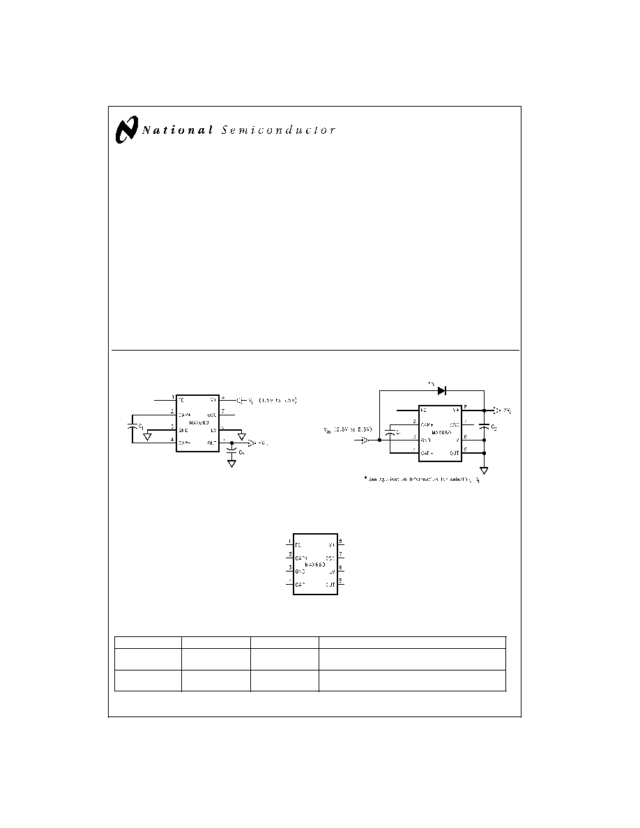
Typical Application Circuits
Connection Diagram
Ordering Information
Order Number
Top Mark
Package
Supplied as
MAX660M
Date Code
MAX660M
M08A
Rail (95 units/rail)
MAX660MX
Date Code
MAX660M
M08A
Tape and Reel (2500 units/rail)
Voltage Inverter
DS100898-1
Positive Voltage Doubler
DS100898-2
8-Lead SO
DS100898-5
Top View
November 1999
MAX660
Switched
Capacitor
V
oltage
Converter
© 1999 National Semiconductor Corporation
DS100898
www.national.com

Absolute Maximum Ratings
(Note 1)
If Military/Aerospace specified devices are required,
please contact the National Semiconductor Sales Office/
Distributors for availability and specifications.
Supply Voltage (V+ to GND, or GND to OUT)
6V
LV
(OUT - 0.3V) to (GND + 3V)
FC, OSC
The least negative of (OUT - 0.3V)
or (V+ - 6V) to (V+ + 0.3V)
V+ and OUT Continuous Output Current
120 mA
Output Short-Circuit Duration to GND (Note 2)
1 sec.
Power Dissipation
(T
A
= 25∞C) (Note 3)
735 mW
T
J
Max (Note 3)
150∞C
JA
(Note 3)
170∞C/W
Operating Junction Temp. Range
-40∞C to +85∞C
Storage Temperature Range
-65∞C to +150∞C
Lead Temperature
300∞C
(Soldering, 10 seconds)
ESD Rating
2 kV
Electrical Characteristics
Limits in standard typeface are for T
J
= 25∞C, and limits in boldface type apply over the full operating temperature range. Un-
less otherwise specified: V+ = 5V, FC = Open, C
1
= C
2
= 150 µF. (Note 4)
Symbol
Parameter
Condition
Min
Typ
Max
Units
V+
Supply Voltage
R
L
= 1k
Inverter, LV = Open
(Note 5)
3.5
5.5
Inverter, LV = GND
1.5
5.5
V
Doubler, LV = OUT
2.5
5.5
I
Q
Supply Current
No Load
FC = Open
0.12
0.5
mA
LV = Open
FC = V+
1
3
I
L
Output Current
T
A
+85∞C, OUT
-4V
100
mA
T
A
>
+85∞C, OUT
-3.8V
100
R
OUT
Output Resistance (Note 6)
I
L
= 100 mA
T
A
+85∞C
6.5
10
T
A
>
+85∞C
12
F
OSC
Oscillator Frequency
OSC = Open
FC = Open
5
10
kHz
FC = V+
40
80
I
OSC
OSC Input Current
FC = Open
±
2
µA
FC = V+
±
16
P
EFF
Power Efficiency
R
L
(1k) between V
+
and OUT
96
98
R
L
(500
) between GND and OUT
92
96
%
I
L
= 100 mA to GND
88
V
OEFF
Voltage Conversion Efficiency
No Load
99
99.96
%
Note 1: Absolute maximum ratings indicate limits beyond which damage to the device may occur. Electrical specifications do not apply when operating the device
beyond its rated operating conditions.
Note 2: OUT may be shorted to GND for one second without damage. However, shorting OUT to V+ may damage the device and should be avoided. Also, for tem-
peratures above 85∞C, OUT must not be shorted to GND or V+, or device may be damaged.
Note 3: The maximum allowable power dissipation is calculated by using P
DMax
= (T
JMax
- T
A
)/
JA
, where T
JMax
is the maximum junction temperature, T
A
is the
ambient temperature, and
JA
is the junction-to-ambient thermal resistance of the specified package.
Note 4: In the test circuit, capacitors C
1
and C
2
are 0.2
maximum ESR capacitors. Capacitors with higher ESR will increase output resistance, reduce output volt-
age and efficiency.
Note 5: The minimum limit for this parameter is different from the limit of 3.0V for the industry-standard "660" product. For inverter operation with supply voltage be-
low 3.5V, connect the LV pin to GND.
Note 6: Specified output resistance includes internal switch resistance and capacitor ESR.
MAX660
www.national.com
2

Test Circuit
Typical Performance Characteristics
(Circuit of
Figure 1)
DS100898-4
FIGURE 1. MAX660 Test Circuit
Supply Current vs
Supply Voltage
DS100898-36
Supply Current vs
Oscillator Frequency
DS100898-37
Output Source Resistance
vs Supply Voltage
DS100898-38
Output Source Resistance
vs Temperature
DS100898-39
Efficiency vs Load
Load Current
DS100898-40
Output Voltage Drop
vs Load Current
DS100898-41
MAX660
www.national.com
3

Typical Performance Characteristics
(Circuit of
Figure 1) (Continued)
Efficiency vs
Oscillator Frequency
DS100898-13
Output Voltage vs
Oscillator Frequency
DS100898-14
Oscillator Frequency
vs External Capacitance
DS100898-15
Oscillator Frequency
Supply Voltage
(FC = V+)
DS100898-16
Oscillator Frequency vs
Supply Voltage
(FC = Open)
DS100898-17
Oscillator Frequency vs
Temperature
(FC = V+)
DS100898-18
Oscillator Frequency
vs Temperature
(FC = Open)
DS100898-19
MAX660
www.national.com
4

Pin Description
Pin
Name
Function
Voltage Inverter
Voltage Doubler
1
FC
Frequency control for internal oscillator:
Same as inverter.
FC = open, f
OSC
= 10 kHz (typ);
FC = V+, f
OSC
= 80 kHz (typ);
FC has no effect when OSC pin is driven externally.
2
CAP+
Connect this pin to the positive terminal of
charge-pump capacitor.
Same as inverter.
3
GND
Power supply ground input.
Power supply positive voltage input.
4
CAP-
Connect this pin to the negative terminal of
charge-pump capacitor.
Same as inverter.
5
OUT
Negative voltage output.
Power supply ground input.
6
LV
Low-voltage operation input. Tie LV to GND when
input voltage is less than 3.5V. Above 3.5V, LV can
be connected to GND or left open. When driving
OSC with an external clock, LV must be connected
to GND.
LV must be tied to OUT.
7
OSC
Oscillator control input. OSC is connected to an
internal 15 pF capacitor. An external capacitor can
be connected to slow the oscillator. Also, an
external clock can be used to drive OSC.
Same as inverter except that OSC cannot be driven
by an external clock.
8
V+
Power supply positive voltage input.
Positive voltage output.
Circuit Description
The MAX660 contains four large CMOS switches which are
switched in a sequence to invert the input supply voltage.
Energy transfer and storage are provided by external capaci-
tors.
Figure 2 illustrates the voltage conversion scheme.
When S
1
and S
3
are closed, C
1
charges to the supply volt-
age V+. During this time interval switches S
2
and S
4
are
open. In the second time interval, S
1
and S
3
are open and S
2
and S
4
are closed, C
1
is charging C
2
. After a number of
cycles, the voltage across C
2
will be pumped to V+. Since
the anode of C
2
is connected to ground, the output at the
cathode of C
2
equals -(V+) assuming no load on C
2
, no loss
in the switches, and no ESR in the capacitors. In reality, the
charge transfer efficiency depends on the switching fre-
quency, the on-resistance of the switches, and the ESR of
the capacitors.
Application Information
SIMPLE NEGATIVE VOLTAGE CONVERTER
The main application of MAX660 is to generate a negative
supply voltage. The voltage inverter circuit uses only two ex-
ternal capacitors as shown in the Typical Application Circuits.
The range of the input supply voltage is 1.5V to 5.5V. For a
supply voltage less than 3.5V, the LV pin must be connected
to ground to bypass the internal regulator circuitry. This gives
the best performance in low voltage applications. If the sup-
ply voltage is greater than 3.5V, LV may be connected to
ground or left open. The choice of leaving LV open simplifies
the direct substitution of the MAX660 for the LMC7660
Switched Capacitor Voltage Converter.
The output characteristics of this circuit can be approximated
by an ideal voltage source in series with a resistor. The volt-
age source equals -(V+). The output resistance R
out
is a
function of the ON resistance of the internal MOS switches,
the oscillator frequency, and the capacitance and ESR of C
1
and C
2
. A good approximation is:
where R
SW
is the sum of the ON resistance of the internal
MOS switches shown in
Figure 2.
High value, low ESR capacitors will reduce the output resis-
tance. Instead of increasing the capacitance, the oscillator
frequency can be increased to reduce the 2/(f
osc
x C
1
) term.
Once this term is trivial compared with R
SW
and ESRs, fur-
ther increasing in oscillator frequency and capacitance will
become ineffective.
The peak-to-peak output voltage ripple is determined by the
oscillator frequency, and the capacitance and ESR of the
output capacitor C
2
:
DS100898-21
FIGURE 2. Voltage Inverting Principle
MAX660
www.national.com
5