TL C 8652
PC16550D
Universal
Asynchronous
ReceiverTransmitter
with
FIFOs
June 1995
PC16550D Universal Asynchronous
Receiver Transmitter with FIFOs
General Description
The PC16550D is an improved version of the original 16450
Universal
Asynchronous
Receiver Transmitter
(UART)
Functionally identical to the 16450 on powerup (CHARAC-
TER mode)
the PC16550D can be put into an alternate
mode (FIFO mode) to relieve the CPU of excessive software
overhead
In this mode internal FIFOs are activated allowing 16 bytes
(plus 3 bits of error data per byte in the RCVR FIFO) to be
stored in both receive and transmit modes All the logic is on
chip to minimize system overhead and maximize system ef-
ficiency Two pin functions have been changed to allow sig-
nalling of DMA transfers
The UART performs serial-to-parallel conversion on data
characters received from a peripheral device or a MODEM
and parallel-to-serial conversion on data characters re-
ceived from the CPU The CPU can read the complete
status of the UART at any time during the functional opera-
tion Status information reported includes the type and con-
dition of the transfer operations being performed by the
UART as well as any error conditions (parity overrun fram-
ing or break interrupt)
The UART includes a programmable baud rate generator
that is capable of dividing the timing reference clock input
by divisors of 1 to (2
16
b
1) and producing a 16
c
clock for
driving the internal transmitter logic Provisions are also in-
cluded to use this 16
c
clock to drive the receiver logic The
UART has complete MODEM-control capability and a proc-
essor-interrupt system Interrupts can be programmed to
the user's requirements minimizing the computing required
to handle the communications link
The UART is fabricated using National Semiconductor's ad-
vanced M
2
CMOS process
Can also be reset to 16450 Mode under software control
Note This part is patented
Features
Y
Capable of running all existing 16450 software
Y
Pin for pin compatible with the existing 16450 except
for CSOUT (24) and NC (29) The former CSOUT and
NC pins are TXRDY and RXRDY respectively
Y
After reset all registers are identical to the 16450 reg-
ister set
Y
In the FIFO mode transmitter and receiver are each
buffered with 16 byte FIFO's to reduce the number of
interrrupts presented to the CPU
Y
Adds or deletes standard asynchronous communication
bits (start stop and parity) to or from the serial data
Y
Holding and shift registers in the 16450 Mode eliminate
the need for precise synchronization between the CPU
and serial data
Y
Independently controlled transmit receive line status
and data set interrupts
Y
Programmable baud generator divides any input clock
by 1 to (2
16
b
1) and generates the 16
c
clock
Y
Independent receiver clock input
Y
MODEM control functions (CTS RTS DSR DTR RI
and DCD)
Y
Fully programmable serial-interface characteristics
5- 6- 7- or 8-bit characters
Even odd or no-parity bit generation and detection
1- 1
- or 2-stop bit generation
Baud generation (DC to 1 5M baud)
Y
False start bit detection
Y
Complete status reporting capabilities
Y
TRI-STATE
TTL drive for the data and control buses
Y
Line break generation and detection
Y
Internal diagnostic capabilities
Loopback controls for communications link fault
isolation
Break parity overrun framing error simulation
Y
Full prioritized interrupt system controls
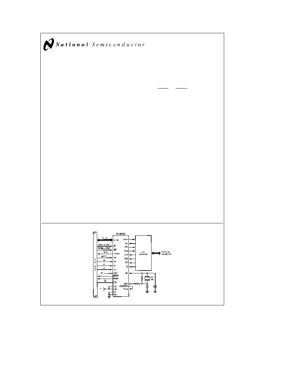
Basic Configuration
TL C 8652 ≠ 1
TRI-STATE
is a registered trademark of National Semiconductor Corp
C1995 National Semiconductor Corporation
RRD-B30M75 Printed in U S A

Table of Contents
1 0 ABSOLUTE MAXIMUM RATINGS
2 0 DC ELECTRICAL CHARACTERISTICS
3 0 AC ELECTRICAL CHARACTERISTICS
4 0 TIMING WAVEFORMS
5 0 BLOCK DIAGRAM
6 0 PIN DESCRIPTIONS
7 0 CONNECTION DIAGRAMS
8 0 REGISTERS
8 1 Line Control Register
8 2 Typical Clock Circuits
8 0 REGISTERS
(Continued)
8 3 Programmable Baud Generator
8 4 Line Status Register
8 5 FIFO Control Register
8 6 Interrupt Identification Register
8 7 Interrupt Enable Register
8 8 Modem Control Register
8 9 Modem Status Register
8 10 Scratchpad Register
8 11 FIFO Interrupt Mode Operation
8 12 FIFO Polled Mode Operation
9 0 TYPICAL APPLICATIONS
2

1 0
Absolute Maximum Ratings
Temperature Under Bias
0 C to
a
70 C
Storage Temperature
b
65 C to
a
150 C
All Input or Output Voltages
with Respect to V
SS
b
0 5V to
a
7 0V
Power Dissipation
1W
Note
Maximum ratings indicate limits beyond which perma-
nent damage may occur Continuous operation at these lim-
its is not intended and should be limited to those conditions
specified under DC electrical characteristics
2 0
DC Electrical Characteristics
T
A
e
0 C to
a
70 C V
DD
e a
5V
g
10% V
SS
e
0V unless otherwise specified
Symbol
Parameter
Conditions
Min
Max
Units
V
ILX
Clock Input Low Voltage
b
0 5
0 8
V
V
IHX
Clock Input High Voltage
2 0
V
DD
V
V
IL
Input Low Voltage
b
0 5
0 8
V
V
IH
Input High Voltage
2 0
V
DD
V
V
OL
Output Low Voltage
I
OL
e
1 6 mA on all (Note 1)
0 4
V
V
OH
Output High Voltage
I
OH
e b
1 0 mA (Note 1)
2 4
V
I
CC
(AV)
Average Power Supply
V
DD
e
5 5V T
A
e
25 C
Current
No Loads on output
SIN DSR DCD
15
mA
CTS RI
e
2 0V
All other inputs
e
0 8V
I
IL
Input Leakage
V
DD
e
5 5V V
SS
e
0V
g
10
m
A
I
CL
Clock Leakage
All other pins floating
g
10
m
A
V
IN
e
0V 5 5V
I
OZ
TRI-STATE Leakage
V
DD
e
5 5V V
SS
e
0V
V
OUT
e
0V 5 25V
1) Chip deselected
g
20
m
A
2) WRITE mode
chip selected
V
ILMR
MR Schmitt V
IL
0 8
V
V
IHMR
MR Schmitt V
IH
2 0
V
Note 1
Does not apply to XOUT
Capacitance
T
A
e
25 C V
DD
e
V
SS
e
0V
Symbol
Parameter
Conditions
Min
Typ
Max
Units
C
XIN
Clock Input Capacitance
7
9
pF
f
c
e
1 MHz
C
XOUT
Clock Output Capacitance
7
9
pF
Unmeasured pins
C
IN
Input Capacitance
5
7
pF
returned to V
SS
C
OUT
Output Capacitance
6
8
pF
C
I O
Input Output Capacitance
10
12
pF
3

3 0
AC Electrical Characteristics
T
A
e
0 C to
a
70 C V
DD
e a
5V
g
10%
Symbol
Parameter
Conditions
Min
Max
Units
t
ADS
Address Strobe Width
60
ns
t
AH
Address Hold Time
0
ns
t
AR
RD RD Delay from Address
(Note 1)
30
ns
t
AS
Address Setup Time
60
ns
t
AW
WR WR Delay from Address
(Note 1)
30
ns
t
CH
Chip Select Hold Time
0
ns
t
CS
Chip Select Setup Time
60
ns
t
CSR
RD RD Delay from Chip Select
(Note 1)
30
ns
t
CSW
WR WR Delay from Select
(Note 1)
30
ns
t
DH
Data Hold Time
30
ns
t
DS
Data Setup Time
30
ns
t
HZ
RD RD to Floating Data Delay
100 pF loading (Note 3)
0
100
ns
t
MR
Master Reset Pulse Width
5000
ns
t
RA
Address Hold Time from RD RD
(Note 1)
20
ns
t
RC
Read Cycle Delay
125
ns
t
RCS
Chip Select Hold Time from RD RD
(Note 1)
20
ns
t
RD
RD RD Strobe Width
125
ns
t
RDD
RD RD to Driver Enable Disable
100 pF loading (Note 3)
60
ns
t
RVD
Delay from RD RD to Data
100 pF loading
60
ns
t
WA
Address Hold Time from WR WR
(Note 1)
20
ns
t
WC
Write Cycle Delay
150
ns
t
WCS
Chip Select Hold Time from WR WR
(Note 1)
20
ns
t
WR
WR WR Strobe Width
100
ns
t
XH
Duration of Clock High Pulse
External Clock (8 Max )
55
ns
t
XL
Duration of Clock Low Pulse
External Clock (8 Max )
55
ns
RC
Read Cycle
e
t
AR
a
t
RD
a
t
RC
280
ns
WC
Write Cycle
e
t
AW
a
t
WR
a
t
WC
280
ns
Baud Generator
N
Baud Divisor
1
2
16
b
1
t
BHD
Baud Output Positive Edge Delay
100 pF Load
175
ns
t
BLD
Baud Output Negative Edge Delay
100 pF Load
175
ns
t
HW
Baud Output Up Time
f
X
e
8
d
2 100 pF Load
75
ns
t
LW
Baud Output Down Time
f
X
e
8
d
2 100 pF Load
100
ns
Receiver
t
RAI
Delay from Active Edge
ns
of RD to Reset Interrupt
t
RINT
Delay from RD RD
100 pF Load
(RD RBR or RD LSR)
1000
ns
to Reset Interrupt
t
RXI
Delay from RD RBR
290
ns
to RXRDY Inactive
t
SCD
Delay from RCLK to Sample Time
2000
ns
t
SINT
Delay from Stop to Set Interrupt
(Note 2)
1
RCLK
Cycles
Note 1
Applicable only when ADS is tied low
Note 2
In the FIFO mode (FCR0
e
1) the trigger level interrupts the receiver data available indication the active RXRDY indication and the overrun error indication
will be delayed 3 RCLKs Status indicators (PE FE BI) will be delayed 3 RCLKs after the first byte has been received For subsequently received bytes these
indicators will be updated immediately after RDRBR goes inactive Timeout interrupt is delayed 8 RCLKs
Note 3
Charge and discharge time is determined by V
OL
V
OH
and the external loading
Note 4
These specifications are preliminary
4
3 0
AC Electrical Characteristics
(Continued)
Symbol
Parameter
Conditions
Min
Max
Units
Transmitter
t
HR
Delay from WR WR (WR THR)
100 pF Load
175
ns
to Reset Interrupt
t
IR
Delay from RD RD (RD IIR) to Reset
100 pF Load
250
ns
Interrupt (THRE)
t
IRS
Delay from Initial INTR Reset to Transmit
8
24
BAUDOUT
Start
Cycles
t
SI
Delay from Initial Write to Interrupt
(Note 1)
16
24
BAUDOUT
Cycles
t
STI
Delay from Stop to Interrupt (THRE)
(Note 1)
8
8
BAUDOUT
Cycles
t
SXA
Delay from Start to TXRDY active
100 pF Load
8
BAUDOUT
Cycles
t
WXI
Delay from Write to TXRDY inactive
100 pF Load
195
ns
Modem Control
t
MDO
Delay from WR WR (WR MCR) to
100 pF Load
200
ns
Output
t
RIM
Delay from RD RD to Reset Interrupt
100 pF Load
250
ns
(RD MSR)
t
SIM
Delay from MODEM Input to Set Interrupt
100 pF Load
250
ns
Note 1
This delay will be lengthened by 1 character time minus the last stop bit time if the transmitter interrupt delay circuit is active (See FIFO Interrupt Mode
Operation)
Note 2
These specifications are preliminary
4 0
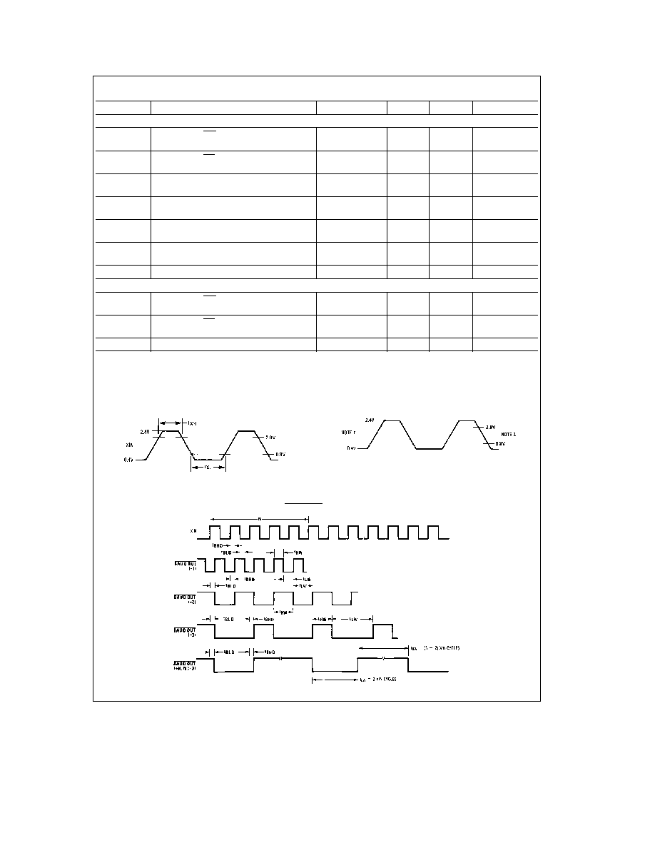
Timing Waveforms
(All timings are referenced to valid 0 and valid 1)
External Clock Input (24 0 MHz Max )
TL C 8652 ≠ 2
AC Test Points
TL C 8652 ≠ 3
Note 1
The 2 4V and 0 4V levels are the voltages that the inputs are driven to during AC testing
Note 2
The 2 0V and 0 8V levels are the voltages at which the timing tests are made
BAUDOUT Timing
TL C 8652 ≠ 4
5