TL F 11928
QR0001
QuickRing
Data
Stream
Controller
PRELIMINARY
October 1994
QR0001
QuickRing
TM
Data Stream Controller
General Description
QuickRing is a point-to-point data transfer architecture de-
signed to facilitate high speed data streams The QuickRing
architecture can be applied both inside the chassis as well
as outside the chassis environments to increase data
throughput Each QR0001 QuickRing Controller node in the
ring is capable of streaming up to 231 MSamples s per sig-
nal line simultaneously including protocol overhead This
device is intended for use in applications that handle high-
bandwidth data streams associated with graphics uncom-
pressed video disk arrays high-speed local area networks
multiprocessor systems and to interconnect peripherals
over a few meters of cable The QR0001 QuickRing Con-
troller can be used to augment the performance of tradition-
al backplane buses in personal computers workstations
and high-end systems The QR0001 is useful for routing
high-bandwidth streams in systems that are larger or topo-
logically more complex than bus-based systems
Features
Y
160-pin PQFP package
Y
16 node single ring capability
Y
Peak theoretical rate over 1 GByte sec for 16 node
ring
Y
Support for Multi-Ring topologies
Y
Error detection detects 1- and 2-bit errors
RING INTERFACE
Y
Precision PLL captures data at 231 MSamples s max
Y
33 MHz maximum ring clock frequency
Y
Low Voltage Differential Signaling (LVDS) ring interface
(IEEE P1596 3)
CLIENT INTERFACE
Y
132 MBytes s data transfer rate at both Tx and Rx
ports
Y
32-bit transmit and receive data ports
Y
Readable internal diagnostic register
Y
TTL signal interface
Block Diagram
TL F 11928 � 1
QuickRing
TM
is a trademark of Apple Computer Incorporated
C1995 National Semiconductor Corporation
RRD-B30M75 Printed in U S A

Table of Contents
1 0
SIGNAL DESCRIPTION
2 0
BASIC STRUCTURE
3 0
CLIENT INTERFACE
3 1
Type and Symbol Fields at the Client Ports
3 2
Client Transmit Port
3 3
Transmit Port Timing Relationships
3 4
Client Receive Port
3 5
Receive Port Timing Relationships
3 5 1 Client Receive Port Interface
Recommendations (PIPE asserted)
3 6
Client Interface Field Definitions
3 7
Client Type Fields
3 8
Transmit Port Head Fields
3 9
Receive Port Head Fields
3 10 Payload Symbols at the Rx and Tx Ports
3 11 Null Symbols at the Rx and Tx Ports
3 12 The HOP fields and the Uniqueness of
Symbol Streams
3 13 Summary of Client Port Field Format
3 14 Readable Registers
3 15 Error Detection
4 0
RING INTERFACE
4 1
Type and Symbol Field at the Ring Ports
4 2
Data and Frames
4 3
Symbol Flux on Ring
4 4
Data on the Ring (Head Payload Tail)
4 5
Access on the Ring
(Voucher Ticket Abort Null)
4 6
Mapping of Type Frame Data and EDC Code
on the Ring
4 7
Ring Interface Field Definitions
4 8
Routing Symbols are Common to All Ports
4 9
Ring Type Fields
4 10 Head Symbol on the Ring
4 11 Payload Symbols on the Ring
4 12 Tail Symbol on the Ring
4 13 Access Symbols on the Ring
4 14 Summary of Ring Port Field Format
5 0 CLOCK SIGNALS
6 0 ABORT SIGNAL
7 0 BRIDGES
8 0 LITTLE BIG ENDIAN ISSUES
9 0 RESET AND INITIALLZATION
9 1 Reset
9 2 Node 0 Selection and Initialization
9 3 Node ID Assignment
9 4 Sequence for Node 0
9 5 Sequence for All Qther Nodes on Ring
10 0 QR0001 OPERATION FLOW
10 1 Ring Traffic Flow Priorities for DnSS port
Transmissions
10 2 Inside the Source Node (Device Transmitting Data)
10 3 Summary of Source Node Actions
10 4 Inside the Target Node
10 5 Summary of Target Node Actions
11 0 BOARD CONSIDERATIONS
11 1 Upstream Port Signal Termination
11 2 QuickRing Physical Layer Details
12 0 POWER AND DECOUPLING ISSUES
12 1 Power Issues
12 2 Decoupling Issues
13 0 DC ELECTRICAL CHARACTERISTICS
14 0 AC TIMING PARAMETERS
15 0 CONNECTION DIAGRAM
16 0 GLOSSARY
17 0 REVISION NOTES
2

1 0 Signal Description
Pin Name
I O
No
Description
RESET
I
1
RESET
When this input is released the initialization sequence begins
ABORT
O
1
ABORT
When asserted it indicates that a failure was detected ABORT is negated by asserting Reset
PIPE
I
1
PIPE
When PIPE is negated (non-pipelined timing) at the Client ports both the symbol and type fields
correspond to each other during the same clock cycle When PIPE is asserted (pipelined timing) the
timing of the Type field leads by one clock at the receive port and trails by one clock at the transmit port
(The type and symbol fields are pipelined )
NODE0
I
1
NODE0
When asserted the controller is configured as having Node ID 0 Node 0 is responsible for
governing the initialization process in the ring
RGCLK
I
1
RING CLOCK
This clock input is the time-base for the ring interface A clock input should be present
when the CKSRC pin is asserted When CKSRC is negated RGCLK should be tied low
CKSRC
I
1
CLOCK SOURCE
Designates the source of the ring clock When asserted RGCLK is the clock source
used for the Ring interface When this pin is negated the clock is derived from the differential UpCLK
CLKOUT
O
1
CLOCK OUT
If CKSRC is asserted then CLKOUT is frequency-locked to the RGCLK If CKSRC is
negated then CLKOUT is frequency-locked to the UpCLK
UpCLK
I
2
UPSTREAM CLOCK
This LVDS input clock comes from the neighbor upstream node and drives the
ring interface when CKSRC is negated
UpSS 5 0
I
12
UPSTREAM SUB-SYMBOL
These 6 LVDS inputs for the Ring interface carry the divided 42-bit symbol
from the downstream port of the previous node
DnCLK
O
2
DOWNSTREAM CLOCK
This LVDS output clock signal is derived from the clock that drives the Ring
interface The transitions on the DnSS are in phase with transitions on the DnCLK signal
DnSS 5 0
O
12
DOWNSTREAM SUB-SYMBOL
These 6 LVDS outputs for the Ring interface carry the divided 42-bit
symbol for the upstream port of the next node
TxCLK
I
1
TRANSMIT CLOCK
On the Client interface all transmit port signals are synchronous to the rising edge
of this clock
TxT 1 0
I
2
TRANSMIT TYPE
On the Client interface this field defines (as head data frame or null) the contents
of TxS
in the previous clock cycle when PIPE is asserted plpelined timing
in the current clock cycle when PIPE is negated non-plpelined timing
TxS 31 01
I
32
TRANSMIT SYMBOL
On the Client interface these signals form the data path of the transmit port
TxOK
O
1
TRANSMIT OKAY
On the Client interface this is the transmit port status signal It tells the client
whether or not another non-null symbol can be accepted Loading of non-null symbols must cease
within 20 symbols of the negation of TxOK Transmission may not resume until TxOK is reasserted
RxCLK
I
1
RECEIVE CLOCK
On the Client interface all receive port signals are synchronous to the rising edge of
this clock Except RxSTALL which is sampled on the following edge of RxCLK
RxT 1 0
O
2
RECEIVE TYPE
On the Client interface this field defines (as head data frame or null) the contents of
RxS
in the next clock cycle for when PIPE is asserted pipelined timing
in the current clock cycle when PIPE is negated non-pipelined timing
RxS 31 0
O
32
RECEIVE SYMBOL
On the Client interface these signals form the data path of the receive port
3

1 0 Signal Description
(Continued)
Pin Name
I O
No
Description
RxSTALL
I
1
RECEIVE STALL
On the Client interface when RxSTALL is asserted
When PIPE is asserted pipelined timing RxS shall remain for the next clock cycle
When PIPE is negated non-pipelined timing RxT will indicate a null for the next clock cycle and RxS
shall remain
RxOE
I
1
RECEIVE OUTPUT ENABLE
On the Client interface when asserted this signal enables outputs
RxS 31-0 When negated the RxS are TRI-STATE
RxET 1 0
O
2
RECEIVE EARLY TYPE
On the Client interface this field identifies in advance whether the information
entering the Rx Port block is a head data frame or null
RxNBL
O
4
RECEIVE NIBBLE
On the Client interface it contains one of the 16 selectable fields of two readable
3 0
internal areas (Diagnostics bits RxS driver)
RxSEL
I
4
RECEIVE SELECT
On the Client interface selects one of the 16 fields appearing on the RxNBL Codes
3 0
from 0 to 7 select 4 bit fields at the current output driver of RxS codes of 8 or above select internal
diagnostics status bits
V
CC
N A
13
POWER PINS
GND
N A
29
GROUND PINS
Note 1
SignalName The indicates that the signal is active low
The following sections assume a 50 MHz ring clock Note that the QR0001 has a maximum ring clock frequency of 33 MHz
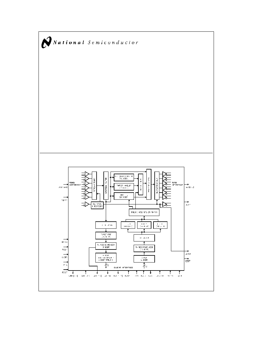
2 0 Basic Structure
The QuickRing Controller has two interfaces the Ring Inter-
face and the Client Interface Each interface has two ports
All ports on the QR0001 are unidirectional so that incoming
and outgoing data can be queued simultaneously
The two Ring interface ports are
1 upstream port for arriving traffic
2 downstream port for departing traffic
The Ring Interface forms the link to other nodes on the
point-to-point QuickRing architecture QuickRing connects
multiple nodes by attaching the upstream port of each node
to the downstream port of another node The ring ports
upstream and downstream are 6 bits wide plus a clock The
ring interface is implemented using LVDS drivers and re-
ceivers The Ring Interface signals are not accessible from
the board except through the controller The on board logic
connects to the QR0001 controller via the Client interface
The two Client Interface ports are
1 the transmit port for locally generated symbol streams
and
2 the receive port for locally-absorbed symbol streams
The transmit and receive ports have a 32-bit data path
which use TTL compatible I Os The Transmit (Tx) and Re-
ceive (Rx) ports each have a separate clock plus control
signals for information flow Also some QR0001 internal
status bits can be read through the receive interface All on
board circuitry interfaces to the Client transmit and receive
ports never to the Ring ports
TL F 11928 � 2
FIGURE 2 1 The QuickRing Controller has four ports
QuickRing transmits data streams between nodes on the
ring The goal of QuickRing is to pipeline data streams and
not just to facilitate memory access Imagine connecting
two cards together via a FIFO chip One card can load data
into its side of the FIFO and the other card can extract data
from the other side of the FIFO QuickRing is logically equiv-
alent to placing a large FIFO between pairs of QuickRing
nodes Cards connected through QuickRing form a ring Re-
fer to
Figure 2 2
4

2 0 Basic Structure
TL F 11928 � 10
FIGURE 2 2 Logical Data flow
(QuickRing Virtual FIFOs)
Figure 2 3 shows that data physically moves in a ring from
card to card data traverses the ring until it arrives at the
final destination Physical data flow is unidirectional and
propagates downstream between nearest neighbors
TL F 11928 � 3
FIGURE 2 3 Physical Data Flow in QuickRing
TL F 11928 � 4
FIGURE 2 4 A Sub-Symbol is Multiplexed Every 2 9 ns
The ring formed by connecting Up and Dn ports of adjacent
QuickRing controllers
carries one 42-bit symbol every
20 ns The 42-bit symbol is composed of
32 bits of data
1 Frame bit
2 control bits and
7 bits of EDC
To transmit 42 bits in 20 ns QuickRing divides the 42-bit
symbol into 7 sub-symbols each sub-symbol is 6 bits wide
The controller then multiplexes the sub-symbols onto the 6
LVDS pairs on the downstream port A 7th LVDS clock sig-
nal at 50 MHz (maximum) accompanies every 42-bit sym-
bol transmission Refer to
Figure 2 4
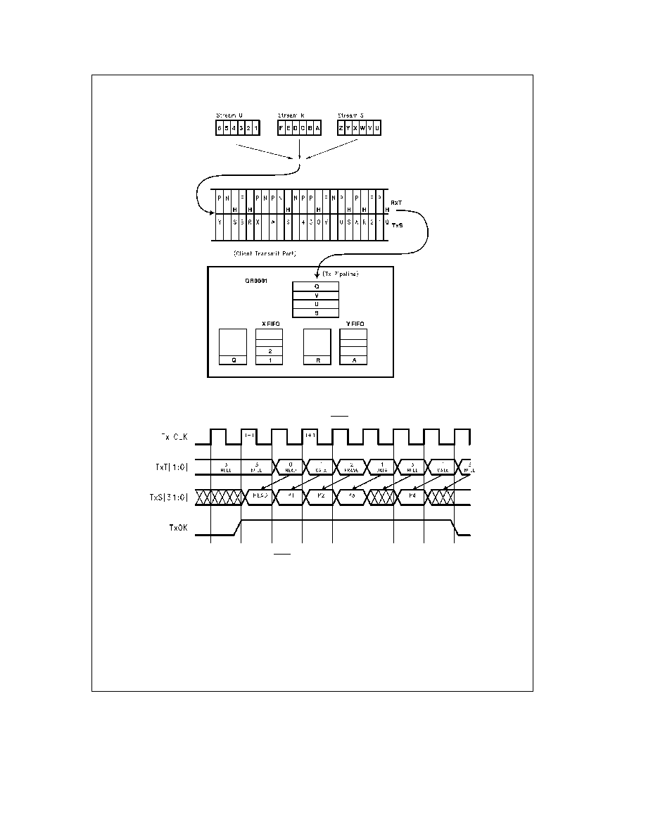
3 0 Client Interface
3 1 Type and Symbol Fields at the Client Ports
The QuickRing client can multiplex multiple independent
data streams onto and from the transmit (Tx) and receive
(Rx) ports of the controller The type fields (TxT 1 01
RxT 1 01 ) distinguishes the contents of the symbol (main
data) fields (TxS 31 0
RxS 31 0 ) The type field identifies
the nature of the symbol field information at the 32-bit ports
as head data frame or null
The transmit port can be thought of as the input to a bank of
fast deep FIFOs connected to other nodes on the ring The
receive port can be treated as the output of the bank of
FIFOs connected to other nodes on the ring
Figure 3 1 il-
lustrates the controller's client interface
TL F 11928 � 5
FIGURE 3 1 Client Ports of a QuickRing Controller
3 2 Client Transmit Port
Figure 3 2 shows the block diagram of the transmit port The
transmit block of QR0001 is formed by Tx Port Tx Resyn-
chronizer Tx Router and 3 independent FIFOs All of these
blocks form the transmit pipeline
1 The Tx Port is the first stage into the transmit pipeline
The Transmit port is a 4 deep pipeline
2 The Tx Resynchronizer is a 32-deep asynchronous FIFO
in the path between the Tx Port and the Tx Router
Note
The Tx Resynchronizer will handle the frequency disconnect between
the Tx Port and ring logic This function will be implemented on the
next QuickRing device
QR1001
3 The Tx Router directs the streams to the appropriate
channel efficiently (described later)
4 FIFOs X and Y are meant for handling one independent
high bandwidth stream each and the LB (Low Band-
width) FIFO is meant for low bandwidth transmissions
The FIFOs contain the data frame part of the client
stream (The Head information is held in a separate hold-
ing latch internally )
The sole purpose of providing two normal (high bandwidth)
FIFOs (X and Y) is so that the client may switch from trans-
mitting one stream to another without slowing down or wast-
ing available ring bandwidth during the context switch
On release of RESET any payload symbols at the transmit
port are ignored until the first head symbol is presented at
the input of the Tx Port QR0001 always checks for consec-
utive heads and ignores all redundant heads The type and
symbol fields are latched internally according to the timing
specified by the state of the PIPE signal
When the client starts a transmission it writes a head fol-
lowed by a stream of payloads QR0001 receives these
symbols through the transmit port and directs them to either
the X Y or LB FlFO Any head symbol with the CONN (see
Section 3 6) field equal to 1 is always routed to the LB FIFO
as is every payload symbol following such a head Any other
head with the CONN field equal to 0 and all payloads follow-
ing such a head are routed to either the X or Y FIFO
5

3 0 Client Interface
(Continued)
QR0001 can handle one Independent data stream
through each of the X and Y FIFOs a total of two
streams at once
Even if the FIFO is not full the FIFO will
store data associated only with a single head Multiple data
streams with various heads will not be held in a single FIFO
The subsequent data streams with different heads will be
held in the Tx pipeline until either FlFO X or Y empties and
the data (with the different head) is allowed to further pro-
ceed in the pipeline
5 The LB FIFO Several streams with different heads can
flow through the LB FIFO at one time When several pay-
loads are loaded following a signal head a head will be
generated for each payload
For all transmissions low bandwidth or normal QR0001 will
keep TxOK asserted for as long as there is space for 20 or
more symbols in the transmit pipeline As soon as the trans-
mit pipeline has space for only 20 more symbols TxOK
negates The initial negation of TxOK indicates to the client
interface that it must stop transmitting non-null symbols
soon TxOK is the only handshake mechanism at the trans-
mit port If TxOK asserts again the count is voided and the
client can write to the TxPort as many symbols as it wants If
TxOK negates again the client must stop writing non-null
symbols within 20 valid transactions
TL F 11928 � 14
FIGURE 3 2 Tx Port Client Interface
The client may pause transmission at any time by present-
ing the null symbol code to the transmit port
When the client interface wishes to begin transmission of a
data stream the client first writes a head (H) to the transmit
port From then on every payload symbol (type
e
data or
frame) sent to the transmit port is assumed to belong to the
stream identified by the head The data stream that the cli-
ent writes at the transmit port is unbounded However if a
new head is written to the transmit port the data stream that
follows is associated with the new head If at any time the
client is not prepared to transmit either a payload or a new
head a null symbol (N) may be introduced into the transmit
data stream
Null symbols do not propagate into the
QR0001
QuickRing
controller
Logically
distinct
data
streams can be multiplexed together and loaded into the
QR0001 transmit port The client is free to switch between
source streams at its convenience as long as it introduces
a new head when the switch occurs
Figure 3 3 shows how three independent streams (high
bandwidth) may be multiplexed from the Client Transmit
Port into the QuickRing controller Stream Q goes first
sending 2 payloads It is followed by 1 payload from stream
R then by 2 payloads from stream S Two more symbols
from stream Q are sent etc
3 3 Transmit Port Timing Relationships
When PIPE is asserted (low voltage level) the type field
TxT accompanying the symbol field TxS is loaded into the
controller one clock cycle after the symbol that it identifies
See
Figure 3 4 When a symbol is presented on TxS at time
t then the corresponding code is presented on TxT at time
t
a
1 The purpose of delivering the TxT field one clock cycle
after the symbol is so that a simple synchronous state ma-
chine has one full clock cycle to compute the TxT code
without using extemal latches on the symbol field
When PIPE is negated (high voltage level) the type field
TxT accompanying the symbol field TxS is loaded into the
controller during the same clock cycle as the symbol it iden-
tifies Refer to
Figure 3 5
The TxOK function and timing remains unchanged regard-
less of the level of the PIPE signal Giving a 20 symbol
warning that transmission of non-null symbols may need to
cease
6
3 0 Client Interface
(Continued)
TL F 11928 � 21
FIGURE 3 3 Logically Distinct Streams of Data can be Multiplexed Into the Tx Port
Transmit Port Timing when PIPE is Asserted
TL F 11928 � 6
FIGURE 3 4 When PIPE is asserted the Type Field Lags the
Symbol Field by One Clock Cycle at the Transmit Port
7

3 0 Client Interface
(Continued)
Transmit Port Timing when PIPE is Negated
TL F 11928 � 22
FIGURE 3 5 When PIPE is negated the Type Field and the
Symbol Field are Loaded during the Same Clock Cycle
TL F 11928 � 15
FIGURE 3 6 Rx Port Client Interface
3 4 Client Receive Port
Figure 3 6 shows the QR0001 receive block and part of the
forwarding path
1 The Upstream Router LB Target Handler Target Han-
dler and the Ring FIFO are part of the forwarding path
The LB Target Handler processes LB vouchers targeted
to this node into tickets These tickets are forwarded to
the source node through the downstream port
The Target Handler processes vouchers targeted to this
node into tickets These tickets are forwarded to the
source node through the downstream port
The Ring FIFO stores incoming data from the upstream
port that is intended to be forwarded to other nodes on
the ring when the downstream pipe is allocated to
launching local data generated by this node
Now the receive block
2 The Head Stripper removes all heads except those iden-
tifying the beginning of a stream
3 The Target FIFO reserves space for 3 normal packets
and 6 LB packets
4 The Rx Resynchronizer is an 8-deep FIFO in the path
between Target FIFO and the Rx Port
Note
The Rx Resynchronizer will handle the discontinuity between the cli-
ent interface and the ring logic of the controller This function will be
implemented on the next QuickRing device
QR1001
5 The Rx Port is the last stage between a data stream and
the client interface
On release of Reset the first two non null symbols that
appear at the RxS 31 0 are the node ID of the controller
and the largest maximum ID number on the ring (See Sec-
tion 9 1 )
RxET alerts the client interface up to 20 symbols prior to
the output stage the type of data entering the receive pipe-
line The RxT when PIPE is asserted leads by one clock
the symbol that it identifies thus giving the client a one
clock cycle advance notice of the symbol about to appear at
the RxS 31 0 The client may choose to stall the symbol at
RxS 31 0 if desired
At the Rx Port a contiguous data stream is unbounded and
data belonging to the same head is marked by a single initial
head appearance At the Rx Port there is no evidence of a
packet A new head will appear only when there is a change
in data stream A long data stream transmitted in multiple
packets from one node to another will appear at the Rx
Port as a single head followed by a long data stream unless
broken by a different stream from a third node
In cases where one target node is the subject of multiple
transmissions from several nodes multiple streams marked
by head symbols will appear multiplexed at the Rx Port The
same will occur if one source node is sending different
streams to the same target A stream is treated as a differ-
ent stream if the 32-bit head symbol varies in at least one
bit
8

3 0 Client Interface
(Continued)
3 5 Receive Port Timing Relationships
When PIPE is asserted (low level) the type field RxT at
time t indicates the type of symbol presented at the output
RxS at time t
a
1 See
Figure 3 7 This is true as long as
RxSTALL is negated
If RxSTALL is asserted when PIPE is asserted (pipeline tim-
ing mode)
1 The RxS 31 0 output will stall at the first non-null
symbol encountered in the pipeline after RxSTALL is
asserted
The symbol on RxS will persist through next
clock cycle unless it corresponds to a null symbol The
RxSTALL input signal is only capable of holding a non-
null symbol at the RxS output
The client may need to examine some symbols within the
symbol stream in order to determine their disposition It is
highly desirable to do so without employing added data path
buffering external to the controller QuickRing allows the cli-
ent to examine the contents of the symbol at the RxS output
through a combination of RxSTALL RxSEL and RxNBL
even while the RxS output drivers may be disabled
To further aid in the receive stream management the sym-
bol type field just entering the Rx Port Block of the receive
pipeline is visible on RxET Thereby the client can preview
the symbol type in the receive pipeline before it appears on
the RxS outputs Thus it is possible to detect the presence
of a head data or frame in the pipeline even if up to 19
more symbols are stored ahead of it
When PIPE is negated (high level) then the value of the
type field RxT TxT at time t corresponds to the value of the
symbol field at the same time t (See
Figure 3 8 ) When two
QuickRing controllers are connected to form a bridge the
TxOK is connected to RxSTALL of the other controller
(Currently an external flip-flop may be needed to satisfy the
setup hold times )
If RxSTALL is asserted when PIPE is negated (high level) at
the next positive edge of clock
1 RxT is forced to Null and
2 The RxS 31 0 persists
To summarize the Client Port Timing
At the Rx Port a non-null symbol remains valid at the RxS
output in the presence of RxSTALL
At the Tx Port when TxOK negates it indicates that the
FIFO is nearly full and the client must stop transmission
within 20 non-null symbols
The PIPE input determines how the type fields RxT and
TxT identify a symbol as it appears at RxS and TxS respec-
tively
At the receive port many different arriving streams may be
multiplexed together Every switch to a new stream context
is marked by a new head symbol The multiplexed stream
that is loaded into a controller at a source node is probably
different than the de-multiplexed stream that arrives at the
target node
The QuickRing protocol does not preserve the order of mul-
tiplexed streams but it does preserve the first-in-first-out
ordering of each individual stream
Figure 3 3 relates to Figure 3 9 It shows that even though
stream Q was loaded first in
Figure 3 3 stream R arrives
first in
Figure 3 9 Notice that at the output the order within
each individual stream is preserved
3 5 1 Client Receive Port Interface Recommendations
(PIPE asserted)
It is recommended when interfacing to the Client Receive
Port to hold RxSTALL negated during normal operation
When the Client interface detects a Non-Null type it may
assert RxSTALL during the next clock cycle to stall that
particular symbol and the next Non-Null type (if available)
See
Figure 3 10
BE AWARE that if RxSTALL is asserted during a clock cycle
of a NON-NULL Type that follows (later in time) a NULL
type the Receive Client interface will stall a NULL type for
the next clock cycle A Null Type will be inserted into the
next clock cycle even if the Receive FIFO contains a NON-
NULL type next This could reduce the performance of the
receive client interface by half See
Figure 3 11
9

3 0 Client Interface
(Continued)
Receive Port Timing when PIPE is Asserted
TL F 11928 � 7
FIGURE 3 7 When PIPE is asserted the Type Field Leads the
Symbol Field by one Clock Cycle at the Receive Port
Receive Port Timing when PIPE is Negated
TL F 11928 � 8
FIGURE 3 8 When PIPE Is negated the Type Field and the
Symbol Field are Loaded during the same Clock Cycle
10

3 0 Client Interface
(Continued)
TL F 11928 � 9
FIGURE 3 9 The Individual Ordering of each Stream is Preserved
TL F 11928 � 23
FIGURE 3 10 Holding Head Symbols for 2 Clocks and
Holding Data and Frame Symbols for 1 Clock each
11

3 0 Client Interface
(Continued)
TL F 11928 � 24
FIGURE 3 11 Null Type is Inserted when RxSTALL is Asserted during
the same Clock Cycle as a Null Symbol (i e in above Figure Null
is Inserted after Head Symbol see also Table 3 0 State
9)
TABLE 3 0 Client Receive Port State Table (Pipeline Timing)
Input
Present State
Next State
Output
RxSTALL
T
RxT
Nullout
Stalled
RxT
Nullout
Stalled
Next
RxS
1
F
Null
Null
Null
T
F
F
Sx
1 2 5 6
2
F
Ty
Null
Ty
T
F
F
Sx
3 4 9
3
F
Null
Ty
Null
F
F
T
Sy
1 2 10 11
4
F
Tz
Ty
Tz
F
F
T
Sy
3 4 8
5
T
Null
Null
T
Null
T
T
F
Sx
1 2 5 6
6
T
Ty
Null
T
Ty
T
T
F
Sx
3 4 9
7
T
Ty
Null
F
T
Null
F
T
F
Sx
1 2 7 11
8
T
Ty
F
Ty
F
T
F
Sx
3 4 8
9
T
T
T
Null
F
T
T
Sy
1 2 7 11
10
T
Ty
F
F
F
Ty
T
T
F
Sx
3 4 9
11
T
Null
F
F
Null
F
T
F
Sx
1 2 7 11
RxSTALL Chip input signal which holds non-null data at RxS
T
(Not externally observable ) The type of symbol which should appear on RxT
during the next clock cycle unless
the symbol marked by RxT
is waiting behind another stalled symbol at RxS
RxT
The type code for the symbol that should appear at RxS
during the next clock cycle unless RxS
is currently
non-null and is being stalled by RxSTALL
Nullout
(Not externally observable ) A state variable that is set to TRUE when the current value of RxS
is volatile
not
stallable and subject to being overwritten by an arriving non-null symbol
Stalled
(Not externally observable ) A state variable that takes on the value of RxSTALL during the previous clock cycle
Next
(Not externally observable ) The state machine output that loads the RxS
output with the next non-null value in the
pipeline
RxS
The 32-bit symbol output bus of the Receive Port
T
TRUE
F
FALSE
Null
The symbol type code representing the absence of a symbol
Ty Tz
Symbol type codes for a non-null symbol
Sx
The value of RxS
unchanged from the previous cycle
Sy
The new value of RxS
whose symbol type code appeared on RxT
during the previous clock cycle
The state table on the previous page describes the behavior
of the QR0001 Receive Port For convenience each table
row has been numbered on the left-hand side and each of
the possible next-case rows is listed on the right-hand side
Following the state table is a description of the input output
and state variables as well as of the entries within the state
table
Row number 9 of the state table shows that the next state
always indicates a null symbol on RxT
regardless of
whether or not a non-null symbol is pending behind symbol
Sy This is an
inefficient but legal behavior as no symbol is
lost Unfortunately until RxSTALL is released the Receive
Port will remain in rows 9 7 and 11 none of which will allow
the arrival of the next non-null symbol to be detected on
RxT
Entry number 10 however represents a condition where a
non-null symbol can arrive at and disappear from RxS
without the possibility of being stalled This represents
ille-
gal behavior of the QR0001 Receive Port Entry into the
condition represented by row 10 must be handled specially
or system data loss will result
12
3 0 Client Interface
(Continued)
Workarounds for No-Stall Bug
There are three alternatives available to work around the
no-stall bug (1) Release RxSTALL for one clock cycle only
when RxT
takes on a non-null value leaving RxSTALL
asserted at all other times (2) build a client system that is
guaranteed not to require that any symbol remain on RxS
for more than two clock cycles or (3) provide an external
latch to save symbols that might have been lost due to entry
to row 10 and stall the next symbol in row 7 or 11 until the
external latch can be read
Alternative
1
Leave RxSTALL normally asserted This is
the easiest method It restricts the Receive port to rows 1
2 5 6 and 9 RxSTALL is released only to enter rows 1 and
2 This is easily accomplished by releasing RxSTALL in re-
sponse to each non-null value but only when that value is
no longer needed at RxS
RxT
will remain non-null for
only one clock cycle and this event will have to be remem-
bered by the client state machine Unfortunately because
the next state result of row 9 does not update RxT
the
fastest that a client may receive data is once every other
clock cycle If there is always another symbol ready in the
pipeline then the Receive Port will toggle between rows 9
and 2 and RxS
will be updated only on the exit from row
9
TL F 11928 � 32
Alternative
2
Design a client system that can always
consume a received symbol within two clocks This may be
impractical but if the client system fits this description then
there is no problem This is because the next state of row
10 is entered in order to stall a symbol that just appeared
upon the exit from row 3 and row 10 preserves the symbol
for exactly one more clock cycle Every next-case row out of
row 10 will advance RxS
to the next symbol so the un-
stallable symbol always appears at RxS
for exactly two
clock cycles
Alternative
3
Provide external storage for the volatile
symbol and stall the next symbol at RxS
until the saved
copy can be used The only entrance to row 10 is from row
3 External logic must monitor the interface for the transition
from row 3 to row 10 or 11 and must both save the unstalla-
ble symbol and hold RxSTALL asserted until the external
copy can be used This solution requires that external logic
emulate the QR0001 Receive Port state machine Although
the T'
input variable and the Nullout and Stalled state
variables are not observable on output pins of the chip it is
possible to compute them externally An external state ma-
chine can deterministically compute the previous state and
the value input T'
that helped cause it Although this infor-
mation is available one cycle late there is time to stall the
next symbol until the no-stall symbol register is being freed
up
The advantage of alternative 1 is its simplicity if it is not
necessary to receive symbols more often than once every
other clock cycle The advantage of alternative 2 is that if it
happens to describe your system (if it's free) then you will
not encounter the no-stall bug The advantage of alternative
3 is that the client can keep up with high-bandwidth received
streams that deliver symbols on every clock cycle
3 6 Client Interface Field Definitions
Table 3 1 shows the symbol field definitions for the Tx and
Rx ports Refer to Section 3 13 for details
TABLE 3 1 Tx and Rx Port Symbol Field Definitions
Field
Descriptions
Type 1 0
At the client ports distinguishes head
data frame and null
CONN 1 0
The connection code (CON 1 0 ) provides
two types of transmission normal and low
bandwidth Low-bandwidth streams are
transmitted with higher priority
TRGT 3 0
The target field contains the node ID of the
target of the associated payload
SRCE 3 0
The source field contains the node ID of
the source of the associated payload
HOP1 3 0
They distinguish between unique streams
HOP2 3 0
whose source-to-target routes are
HOP3 3 0
identical In a multiple-ring topology they
HOP4 3 0
supplement source and target ID fields to
HOP5 3 0
route streams as they hop from ring to ring
(See section on Ring of Rings)
At the client ports ACCess field should be 00
The ACC
field is valid only in the ring ports Refer to Sections 4 7 and
4 13 for more details
Table 3 2 shows the values of the connection field
(CONN 1 0 ) If a LB connection is requested QuickRing
parcels the data or frame symbols presented at the Tx Port
and transmits every payload in 2 symbol ring packets 1
head and 1 payload
TABLE 3 2 Connection Field Definitions
CONN 1 0
Name
Description
0
Normal
Queue and accumulate
symbols from the same
stream at will to maximize
system efficiency and
minimize system load
1
Low Band-
Do not concatenate with
other data symbols from the
width (LB)
same stream Results in two
symbol packets head and
payload
2
N A
Reserved
3
N A
Reserved
3 7 Client Type Fields
The TxT 1 0 and RxT 1 0 fields are the type fields at the
transmit and receive ports respectively They are encoded
as shown in Table 3 3 Each 32-bit symbol written or read
from the client ports is associated with one type field
13

3 0 Client Interface
(Continued)
TABLE 3 3 Client Type (TxT RxT) Field Definitions
T 1
T 0
Name
Description
0
0
Head
Associated symbol is a head
symbol
0
1
Data
Associated payload symbol is a
data symbol
1
0
Frame
Associated payload symbol is a
frame symbol
1
1
Null
No associated symbol
3 8 Transmit Port Head Fields
A head symbol must be loaded into the transmit port when-
ever the client wants to start a transmission or when the
context of the loaded symbols is switched to another
stream Redundant heads are acceptable to the controller
transmit port If multiple heads are loaded without interven-
ing data or frame symbols then all but the last head are
ignored The transmit port evaluates the connection target
and all hop fields The controller adds its own ID to the
source field internally based on the local node ID value that
was set during initialization The ACCess field is ignored and
should be set to zero by the client Table 3 4 shows the
format of a head symbol that the local client must load into
the Tx Port to establish a connection
TABLE 3 4 Transmit Port Head Fields
TxT 1 0
TxS 31 0
1 0
31 30 29 28 27 24 23 20 19 16 15 12 11 8
7 4
3 0
Type
Acc
Conn Srce
Trgt
HOP
0
XX
Conn XXXX Trgt Hop1 Hop2 Hop3 Hop4 Hop5
3 9 Receive Port Head Fields
The receive port head symbol format contains the same
fields as are found in heads at the transmit port but are
shifted from their original positions when they exit the re-
ceive port The purpose is to support routing of streams in
multiple-ring topologies Head symbols only appear at the
receive port when there is an actual change of head Re-
dundant head symbols are always deleted Head symbols at
the receive port hold valid information in the connection
source target and all hop fields The ACCess field is unde-
fined and should be ignored by the client
Table 3 5 shows the format of the head field at the receive
port of the controller
TABLE 3 5 Receive Port Head Fields
RxT 1 0
RxS 31 0
1 0
31 30 29 28 27 24 23 20 19 16 15 12 11 8
7 4
3 0
Type
Acc
Conn Trgt
HOP
Srce
0
XX
Conn Trgt Hop1 Hop2 Hop3 Hop4 Hop5 Srce
3 10 Payload Symbols at the Rx and Tx Ports
Payload symbols at the transmit or receive ports follow the
head symbol that identifies them A payload consists of a
sequence of data and or frame symbols that are distin-
guished by a 1 or 2 in the accompanying type field refer to
Table 3 6 The identification of a frame or data symbol is
encoded in the Type field at the Tx and Rx port If the type
field has a value of 1 it is a data symbol and if the value is
2 then it is a frame symbol The type field at the receive
port leads the symbol field that it identifies by one clock
cycle and at the transmit port it lags the symbol field by one
clock when PIPE is asserted However if the controller is in
non-pipelined timing PIPE is negated the type field corre-
sponds to the symbol at the same clock
TABLE 3 6 Payload Symbols at Tx Rx Ports
Type 1 0
Tx Rx S 31 0
1
DATA User Defined Information
2
FRAME User Denfined Information
3 11 Null Symbols at the Rx and Tx Ports
The lack of a head symbol or payload symbol is indicated at
the Rx port by null symbols whose type field is 3 and
whose other bits are undefined outputs or don't care inputs
At the Tx port if a head or payload is not ready to be trans-
mitted a null symbol code should be presented at the TxT
The value of the type fields at the client ports is as indicated
in Table 3 7
TABLE 3 7 Null Symbol Format
Type 1 0
Tx Rx S 1 0
3
NULL Don't Care
3 12 The HOP fields and the Uniqueness of Symbol
Streams
The identity of a symbol stream is fixed by the combination
of the connection source target and hop fields If the
heads of symbol streams differ in any of these fields then
they represent different symbol streams
The symbols of a unique stream will always arrive in order
Multiple streams targeted at the same node may arrive in-
terleaved The interleaving will always be indicated by an
appropriate head symbol identifying the switch in stream
context
The Hop Fields were created to route packets through
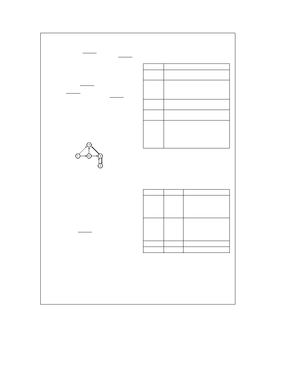
bridges in multiple ring topologies In single ring topologies
they have the function of identifying different streams The
hop fields can be used to distinguish between 2
20
different
data streams in a single ring However in multiple ring topol-
ogies every time a bridge is crossed one hop field is used
Therefore it is lost for identifying unique data streams Ta-
ble 3 8 shows the hop field locations at the transmit port
and Table 3 9 shows the hop fields at the receive port
If the particular node is a bridge to another ring the PIPE
signal should be negated high voltage level The HOP fields
rotate the same regardless of the state of the PIPE input
The actual rotation of the Source Target and HOP fields
occurs at the client receive port see Tables 3 8 3 9 The
HOP fields rotate between the Transmit Client and the Re-
ceive Client as follows (from Receive Client perspective)
Source bits (27 24) shift to bit field (3 0)
All other HOP fields (including Target field) move up one
HOP field to the next more significant 4-bit positions (Ex
HOP 5 moves from (3 0)
x
7 4))
Given this information the system interface should be able
to determine how the Source Target and HOP fields rotate
up to a Ring of Rings architecture including 5 HOPs
14

3 0 Client Interface
(Continued)
When the Client Port Receives a data stream the head con-
tains the path taken by the stream to reach this particular
target To look at the Head and determine where the source
is and how many HOPs the stream encountered requires
knowledge of the ring topology It is assumed that during the
initialization process each node will build up a table of ad-
dresses of all the NODEs in the system When a Head is
received it can be compared to the addresses in the table
to determine the source of the data stream All un-used
HOP fields may be used as Stream ID
TABLE 3 8 HOP Fields at the Tx Port
27 24
23 20
19 16
15 12
11 8
7 4
3 0
Srce
Trgt
Hop 1
Hop 2
Hop 3
Hop 4
Hop 5
TABLE 3 9 HOP Fields at the Rx Port
27 24
23 20
19 16
15 12
11 8
7 4
3 0
Trgt
Hop 1
Hop 2
Hop 3
Hop 4
Hop 5
Srce
15

3 0 Client Interface
(Continued)
3 13 Summary of Client Port Field Formats
TABLE 3 10 Client Port FIeld Formats
Tx Port Head Field
Type
Acc
Conn
Srce
Trgt
HOP
TxT 1 0
TxS 31 30
TxS 29 28
TxS 27 24
TxS 23 20
TxS 19 16
TxS 15 12
TxS 11 8
TxS 7 4
TxS 3 0
0
XX
Conn
XXXX
Trgt
HOP 1
HOP 2
HOP 3
HOP 4
HOP 5
Rx Port Head Field
Type
Acc
Conn
Trgt
HOP
Srce
RxT 1 0
RxS 31 30
RxS 29 28
RxS 27 24
RxS 23 20
RxS 19 16
RxS 15 12
RxS 11 8
RxS 7 4
RxS 3 0
0
XX
Conn
Trgt
HOP1
HOP2
HOP3
HOP4
HOP5
Srce
Tx and Rx Ports Payload Symbols
T 1 0
Tx Rx S 31 0
1
DATA User Defined Information
2
FRAME User Defined Information
Tx and Rx Port Null Symbols
T 1 0
Tx Rx S 31 0
3
Null Don't Care
Node ID Format
RxT 1 0
RxS 31 28
RxS 27 0
non-null
Node ID
1 1 1 1 1 1
1
Max ID Format
RxT 1 0
RxS 31 28
RxS 27 0
non-null
Max ID
1 1 1 1 1 1
1
3 14 Readable Registers
The client can read the two internal registers Diagnostics
Register and Receive Symbol Register at any time through
inputs RxSEL 0 3 and outputs RxNBL 0 3 The RxS regis-
ter can also be read while RxSTALL is asserted RxSEL 0 3
selects a 4-bit field within the 32-bit internal registers and
shows that field on the RxNBL 0 3 outputs Diagnostic er-
ror status bits 18 8 will remain latched until the Quick Ring
is reset
TABLE 3 11 Diagnostics Register (Read Only)
31 19
18 12
11 8
7 4
3 0
Reserved
Syndrome
Error
MaxID
Node ID
Word
Status
S 6 0
Node ID
Address of the Node
MaxID
Largest ID on the ring
Error Status
Individual bits are set depending on the origin
of the error
Bit 8
is set due to an EDC detection
Bit 9
is set due to an Abort symbol received at the up-
stream port
Bit 10
is set due to an error in the packets sequence i e
two consecutive heads (Detected on the upstream port of
the ring )
Bit 11
is set due to an invalid address detected (on the
ring)
Syndrome Word
Points to the bit in error detected through
EDC All zeros if no error(s)
Reserved
Reserved for future expansion
16

3 0 Client Interface
(Continued)
TABLE 3 12 Receive Symbol Register (Read Only)
31 0
The most recent 32 Bits of the RxS received
Table 3 13 gives the decode for reading the various register
bits
TABLE 3 13 Register Access Decode
RxSEL 3 0
RxNBL 3 0
Description
0
RxS 3 0
1
RxS 7 4
2
RxS 11 8
3
RxS 15 12
4
RxS 19 16
5
RxS 23 20
6
RxS 27 24
7
RxS 31 28
8
Diagnostics 3 0
Node ID
9
Diagnostics 7 4
No of Nodes
10
Diagnostics 11 8
Error Status
11
Diagnostics 15 12
Syndrome Word
12
Diagnostics 19 16
Syndrome Word
13
Diagnostics 23 20
Reserved
14
Diagnostics 27 24
Reserved
15
Diagnostics 31 28
Reserved
Note
Bit 19 is reserved
3 15 Error Detection (see also Section 3 16)
The error detection code (EDC) field CB 6 0 provides re-
dundant parity checking to verify symbol integrity The
QR0001 implements a modified Hamming code algorithm
that provides Double Error Detection (DED)
To reduce latency effects this version of the QR0001 pro-
vides the syndrome word that can be read from the Diag-
nostics register to show bit(s) detected in error
The syndrome word S 6 0
consists of the Ex-OR of
the Incoming check bits that were sent within the pack-
et CB 6 0
and new generated check bits for the pack-
et (new generated NGCB 6 0 )
A correct EDC field is transmitted with each symbol emitted
from the downstream port Every symbol that is received at
the upstream port is passed through an EDC checking cir-
cuit Any inconsistency causes the ABORT signal to assert
and an abort symbol to be transmitted at the downstream
port EDC fields are propagated through the chip core as
required to support the above described functionality The
EDC field is not visible at the client ports
The ABORT signal will also be asserted if an illegal address
or illegal sequence of symbols is detected The symbol
which triggers ABORT assertion will contiue to move along
the ring until reaching its target node This requires that the
ring be reset every time an abort is detected The initial
occurrence of an abort is captured in the diagnostic register
No subsequent abort will be logged (until the ring is reset)
Table 3 14 shows the matrix of data bits An ``X'' indicates
the bits that are ``Exclusive-ORed'' to generate each partic-
ular check bit Check bit 6 is generated by ``Exclusive
ORing'' all data and all check bits CB 6 0 form the syn-
drome word
Given a Single or Double bit error the code has the follow-
ing properties
1 If the syndrome word S 6 0 is zero (0) then there is No
Error
2 If any of the syndrome bits S 5 0
is not zero (0) and
S6 is zero
then there is a Double Error The particular
bits in error can not be determined
3 If any of the syndrome bits S 5 0 are not zero (0) and
S6 is one
then there is a Single Error in either the data
or the check bits
If a single bit in S 5 0 is one and S6 is one then the corre-
sponding CB is in error and the data is correct
If more than 1 bit in S 5 0 is set to one and S6 is one then
the syndrome bits point to the data bit in error See columns
of Table 3 14 S 5 0 pinpoints to the position number in the
mapping diagram at which bit is in error
If all remaining bits S 5 0 are zero and S6 is one then CB6
is in error
3 16 QR0001 EDC Errors and Client ``Abort'' Pin Func-
tionality
A bug has been identified in the abort operation The
QR0001 ABORT signal does not match the intended opera-
tion as mentioned above The intended operation is that the
following events will cause the ABORT pin to be asserted
and generate an abort symbol that will propagate around
TABLE 3 14 Error Detection Matrix
35-Bit Data Word
CHECK 35 34 33 32 31 30 29 28 27 26 25 24 23 22 21 20 19 18 17 16 15 14 13 12 11 10 9 8 7 6 5 4 3 2 1
BITS
CB0
X
X
X
X
X
X
X
X
X
X
X
X
X
X
X
X
X X
X X
CB1
X
X
X
X
X
X
X
X
X
X
X
X
X
X
X X
X X
X
CB2
X
X
X
X
X
X
X
X
X
X
X
X
X
X X X
X X X
CB3
X
X
X
X
X
X
X
X
X
X
X
X X X X X X
CB4
X
X
X
X
X
X
X
X
X
X
X
X
X
X
X
CB5
X
X
X
X
X
X
X
X
X
CB6
Exclusive ``OR'' All Data Bits (1 � 35) and All Check Bits (0 � 5)
C6 Aids in DED Double Error Detection
17

3 0 Client Interface
(Continued)
the ring EDC error illegal sequence error and node id out of
maximum range Once an error is detected at any node and
the abort symbol has circulated the ring all diagnostic regis-
ters will log the abort symbol except for the node which
generated it That node will log the original cause of the
error
In QR0001 an EDC error does NOT cause an abort symbol
to be generated on the ring and propagate to all nodes All
other abort conditions do generate the abort symbol at the
downstream port An EDC error is displayed in the diagnos-
tic register and causes the local ABORT pin to be asserted
on all nodes which detect the EDC error The symbol in
error continues to the target Multiple nodes could log an
EDC error but unless the node detects the EDC error it will
not know other nodes have seen an error
In QR1001 (the next device in the QuickRing family of prod-
ucts) when an EDC error is detected the node will assert
ABORT pin The symbol in error will continue to its target
The abort symbol will then be sent downstream Down-
stream nodes may see the symbol that causes EDC errors
and log it They they will see the abort symbol and also log
that in the diagnostic register Since the ABORT pin has
already been asserted by the EDC error condition the abord
symbol will have no affect on the ABORT pin
4 0 Ring Interface
4 1 Type and Symbol Field at the Ring Ports
On the ring path upstream and downstream ports type and
symbol fields organize data transmissions Data on the ring
flows in bounded streams called packets Before data flows
in the ring packets are formed by each controller internally
Packets have one head and one or more payload symbols
Since multiple independent packets can be found inside
one controller and multiplexed at the downstream port a
type field accompanies each symbol Inside a controller
packets can be found that may originate from any other
node on the system The type field marks each symbol as a
head payload tail or access
Figure 4 1 shows a typical
symbol on the ring
4 2 Data and Frames
In QuickRing there are two types of payload symbols data
symbols and frame symbols but their distinction is only of
interest to the clients The QuickRing controller does not
discriminate between them except to preserve their identi-
ty The payload on the ring is 33 bits wide 32 bits of normal
data plus a user client defined Frame bit as the 33rd bit
The frame bit is encoded at the client port type fields and it
is transformed into an actual bit inside QuickRing before
transmission at the down stream port
The Frame bit can be used to identify a special kind of data
of interest to the clients It also can be used to designate
the beginning or end of a stream or to distinguish between
data streams at the client interface
4 3 Symbol Flux on Ring
At the transmit and receive ports the length of a data
stream that is uninterrupted by a head is unbounded On the
ring upstream and downstream ports data is bounded
there is an upper bound that gives the concept of a packet
There are two types of packets normal and low bandwidth
(LB) There is a ring protocol defining the symbol sequence
For normal packets the maximum number of payload sym-
bols associated with one head is fixed at 20 symbols The
largest packet is 21 symbols in all
however packets may
be less than 21 symbols The LB packet consists of a Head
and one payload Tail
4 4 Data on the Ring (Head Payload Tail)
QuickRing transports streams of payload symbols from
source nodes to target nodes through the ring interconnect
QuickRing internally assembles packets from the data that
the client writes into the transmit port This data is eventual-
ly transmitted in packets of 1 to 20 payload symbols A head
symbol precedes the packet and the last payload symbol of
a packet is specially marked as the tail of that packet The
head holds the source and the destination node IDs plus
other information that uniquely identifies the stream to
which the payload symbols belong
Payload symbols consists of 32 bits of user defined informa-
tion plus one 33rd user controllable Frame identifier A pay-
load symbol whose frame bit is set to 1 may be called a
Frame symbol Otherwise it may be referred to as a Data
symbol The Frame identifier the logical 33rd user defined
bit is mapped in SS 3 in sub-symbol t see
Figures 4 2 and
4 3
4 5 Access on the Ring (Voucher Ticket Abort Null)
Before a source node can send a packet permission to
transmit must first be granted by the target node To get
permission to transmit the source node sends a voucher to
the target node To grant permission to transmit the target
node sends a ticket back to the source node This is done
only in response to a voucher When the source node sends
a voucher the target node may (1) absorb the voucher and
return a ticket or (2) return the voucher If the source re-
ceives the ticket then it may send one packet to the target
that returned the ticket If the source received its own re-
turned voucher then it will sink it and retransmit the voucher
after 100 clocks for a new request to transmit The number
of retries for the voucher is unlimited until the target returns
a ticket Under normal circumstances the target should re-
turn a ticket in response to a voucher even if it must save
accumulated vouchers in a queue and issue corresponding
tickets with significant delays The retum of a voucher to its
source should occur only if resources for queuing vouchers
in the target node are exhausted
TL F 11928 � 11
FIGURE 4 1 Many streams from many nodes may be multlplexed onto the ring
Access symbols may appear Interspersed anywhere within a data packet
18

4 0 Ring Interface
(Continued)
An abort symbol identifies the occurrence of a failure such
as (1) an illegal symbol sequence (2) a corrupted symbol or
(3) a node ID for which no node is present The node that
creates the abort symbol deletes it once the abort symbol
has circulated the ring
For every tick of the ring clock every node in the ring re-
ceives one symbol at its upstream port and transmits one
symbol at its downstream port In the absence of any other
symbol a null symbol is transmitted
4 6 Mapping of Type Frame Data and EDC
Code on the Ring
On the ring path a 42-bit symbol is transferred on every tick
of the 50 MHz clock The 42-bit symbol is divided into 7 sub-
symbols 6 bits wide Each sub-symbol is transferred se-
quentially at a rate of 1 sub-symbol every 2 9 ns In all 42
bits are transferred every 20 ns Refer to
Figure 4 2
The type field frame bit and the 3 MSB of the data are
mapped to sub-symbol t Data 28 to 0 are mapped onto
sub-symbols u to y The EDC field CB 6 0 is mapped onto
the last two sub-symbols of y and z See
Figure 4 4
Later in this data sheet reference is made only to the fields
that are muItiplexed onto the SS 5 0 field as they appear
on UpSS and DnSS
Figure 4 2 and 4 3 show when each bit
of any symbol is transmitted or received and in what posi-
tion of the sub-symbol it appears For example F (Frame)
appears on SS 3 during ``sub-symbol t'' Data 0 (D0) ap-
pears on SS 1 during ``y'' the sixth sub-symbol
Note
Figure 4 3 shows that the rising edge of DnCLK is aligned with the
beginning of the next to last sub-symbol of the previous symbol that
gets sent out on DnSS 5 0
TL F 11928 � 25
FIGURE 4 2 Seven Sub-Symbols in one Clock Cycle
TL F 11928 � 12
FIGURE 4 3 Seven Sub-Symbols are Serially Transmitted Every 2 9 ns
TL F 11928 � 13
FIGURE 4 4 Sub-Symbols are Serially Transmitted onto 6 Differential Pairs
19

4 0 Ring Interface
(Continued)
4 7 Ring Interface Field Definitions
QuickRing organizes data with a combination of access
symbols and packet symbols
Access
symbols are vouchers tickets nulls and aborts
Packet
symbols are those that form packets such as heads
and payloads
These symbols can also be grouped into routing symbols
and payload symbols
Routing
symbols hold source and target addresses such as
voucher and ticket for access symbols and heads for pack-
et symbols
Payload
symbols are data or frame they hold the informa-
tion the clients are trying to transmit At the client ports a
type field 01 represents a data symbol a type field of 10
a frame symbol A data or frame symbol at the ring ports are
distinguished by an additional frame bit The payload sym-
bol frame or data at the end of a packet is called a tail and
it is encoded as such in the type field
TABLE 4 1 Dn and Up Stream Port
Symbol Field Definitions
Field
Descriptions
Type 1 0
At the ring ports distinguishes access
head payload and tail
F
The Frame bit appears explicitly only at the
upstream and downstream ports (At the
Tx and Rx ports the frame bit is encoded in
the type fields )
ACC 1 0
The access code (ACC 1 0 ) indicates the
type of access symbol on the ring
Voucher ticket null and abort (Doesn't
apply to Tx or Rx ports )
CONN 1 0
The connection code (CON 1 0 ) provides
to types of transmission normal and low-
band-width Low-bandwidth streams are
transmitted with higher priority
TRGT 3 0
The target field contains the node ID of the
target of the associated payload
SRCE 3 0
The source field contains the node ID of
the source of the associated payload
HOP1 3 0
They distinguish between unique streams
whose source-to-target routes are
HOP2 3 0
identical In a multiple-ring topology they
HOP3 3 0
supplement source and target ID fields to
HOP4 3 0
route streams as they hop from ring to ring
HOP5 3 0
(See section on Ring of Rings)
Table 4 2 shows the possible values that the access field
(ACC 1 0 ) can take The ACC field is valid only in the ring
ports
upstream and downstream
At the client ports
ACCess field should be 00
TABLE 4 2 Access Field Definitions
ACC 1 0
Name
Description
0
Abort
Abort This symbol is forwarded
by all nodes that receive it Upon
receipt of an abort symbol each
node asserts an abort signal
which the client uses to detect
that an error has been detected
somewhere on the ring The
system designer may elect that
all nodes be re-initialized
1
Voucher
Request to reserve target buffer
space
2
Ticket
Ackowledgment of reserved
target buffer space
3
Null
Ignore this symbol
Table 4 3 shows the values of the connection field
(CONN 1 0 ) If a LB connection is requested QuickRing
parcels the data or frame symbols presented at the Tx Port
and transmits every payload in 2 symbol packets 1 head
and 1 payload LB connections carry higher priority than
normal connections
TABLE 4 3 Connection Field Definitions
CONN 1 0
Name
Description
0
Normal
Queue and accumulate
symbols from the same
stream at will to maximize
system efficiency and
minimize system load
1
Low Band-
Do not concatenate with
width (LB)
other data symbols from the
same stream Results in two
symbol packets head and
payload
2
N A
Reserved
3
N A
Reserved
4 8 Routing Symbols are Common to All Ports
At all ports of the controller vouchers tickets and heads
manage the flow of associated payload symbols Nulls and
aborts are special symbols to fill idle time or to indicate an
anomalous situation respectively All symbols on the ring
share a common field format of control and status bits
4 9 Ring Type Fields
The Type fields at the upstream and downstream ports are
mapped onto UpSS DnSS during sub-symbol time t
20
4 0 Ring Interface
(Continued)
TABLE 4 4 Ring Port Type Field
T 1
T 0
Name
Description
0
0
Head
A head symbol appears on Up
or on the Dn Ports
0
1
Payload
A data or frame symbol
appears on the Up or on the Dn
Ports
1
0
Tail
The last payload symbol of a
packet appears on the Up or Dn
Ports
1
1
Access
A Voucher Ticket Abort or Null
symbol is present on the Up or
the Dn Ports
4 10 Head Symbol on the Ring
The Controller regenerates head symbols to mark the start
of packets that it introduces to the ring The head symbol is
regenerated from the head written by the client at the trans-
mit port The number of heads that appear on the ring has
no guaranteed relationship to the number of heads loaded
at the transmit port Head symbols on the ring carry informa-
tion in the connection source target and hop fields Table
4 5 shows the field format for the head symbols on the ring
ports
TABLE 4 5 Packet Head Format at the Ring Ports
Type F 31 30 29 28 27 24 23 20 19 16 15 12 11 8
7 4
3 0
0
0
0
Conn Srce
Trgt Hop 1 Hop 2 Hop 3 Hop 4 Hop 5
4 11 Payload Symbols on the Ring
A type field of 1 identifies the symbol field as a payload
symbol A payload is 33 bits wide The frame bit distin-
guishes frame from data symbols Tables 4 6 and 4 7 show
the field format for payload symbols on the ring
TABLE 4 6 Data Payload Format at the Ring Ports
T(1 0)
F
31 0
1
0
Data Symbol
TABLE 4 7 Frame Payload Format at the Ring Ports
T(1 0)
F
31 0
1
1
Frame Symbol
4 12 Tall Symbol on the Ring
A type field of 2 identifies the symbol field as a tail symbol
which is nothing else but the last payload symbol of a pack-
et A tail may carry frame or data as determined by the
state of the frame bit These format of these symbol are
shown in Tables 4 8 and 4 9
TABLE 4 8 Tall-Data Format at the Ring Ports
T(1 0)
F
31 0
2
0
Data Symbol Acting as a Packet Trail
TABLE 4 9 Tail-Frame Format at the Ring Ports
T(1 0)
F
31 0
2
1
Frame Symbol Acting as a Packet Trail
4 13 Access Symbols on the Ring
The fourth kind of symbols depicted by a type field of 3 are
access symbols There are four kinds of access symbols on
the ring vouchers tickets nulls and aborts These are
identified in Table 4 10 through 4 13
Voucher
Vouchers are sent by source nodes to obtain per-
mission to launch packets of client generated payload sym-
bols QuickRing will send a voucher as soon as there is a
head and a data are loaded at the transmit port Table 4 10
shows the format for a voucher A Type field value of 3
indicating an access symbol and the ACCess field value of 1
indicates that the symbol is a voucher
TABLE 4 10 Ring Port Voucher Field Format
Type F 31 30 29 28 27 24 23 20 19 16 15 12 11 8
7 4
3 0
3
0
0 1
Conn Srce
Trgt Hop 1 Hop 2 Hop 3 Hop 4 Hop 5
Ticket
Tickets are returned by target nodes in response to
vouchers They indicate that the target has reserved FIFO
space for one packet QuickRing will send one packet upon
receipt of one ticket The format for a ticket is shown in
Table 4 11 As in all access symbols the type filed has a
value of 3 In tickets a value of 2 in the ACCess indicates
that the symbol is in fact a ticket
TABLE 4 11 Ring Port Ticket Field Format
Type F 31 30 29 28 27 24 23 20 19 16 15 12 11 8
7 4
3 0
3
0
1 0
Conn Srce
Trgt Hop 1 Hop 2 Hop 3 Hop 4 Hop 5
Null
Null symbols are sent to consume idle time on the ring
The symbol format is shown in Table 4 12 When ever a
controller does not have any payload or other access sym-
bol to send it will send a null symbol at its downstream port
TABLE 4 12 Ring Port Null Field Format
T(1 0)
F
31 30
29 0
3
1
3
XXX
Abort
An abort symbol is sent by any node that detects a
failure of addressing protocol or data integrity during nor-
mal operation the QuickRing ring The symbol format is
shown in Table 4 13
TABLE 4 13 Ring Port Abort Field Format
T(1 0)
F
31 30
29 18
3
0
0
XXX
21

4 0 Ring Interface
(Continued)
4 14 Summary of Ring Port Field Format
TABLE 4 14 Ring Port Field Format
Packet Head Format
Type (1 0)
Frame
31 30
29 28
27 24
23 20
19 16
15 12
11 8
7 4
3 0
Type
F
Acc
Conn
Srce
Trgt
HOP
0
0
0
Conn
Srce
Trgt
HOP 1
HOP 2
HOP 3
HOP 4
HOP 5
Data Payload Format
1
0
Data Symbol
Frame Payload Format
1
1
Frame Symbol
Tail-Data Format
2
0
Data Symbol Acting as a Packet Tail
Tail-Frame Format
2
1
Frame Symbol Acting as a Packet Tail
Voucher Field Format
Type
F
Acc
Conn
Srce
Trgt
HOP
3
0
1
Conn
Srce
Trgt
HOP 1
HOP 2
HOP 3
HOP 4
HOP 5
Ticket Field Format
Type
F
Acc
Conn
Srce
Trgt
HOP
3
0
2
Conn
Srce
Trgt
HOP 1
HOP 2
HOP 3
HOP 4
HOP 5
Null Field Format
Type
F
Acc
29 0
3
1
3
XXXXXXXXXXXXXXXXXXXXXXXXXXXXXX
Abort Field Format
Type
F
Acc
29 0
3
0
0
XXXXXXXXXXXXXXXXXXXXXXXXXXXXXX
22
5 0 Clock Signals
There are four clock domains in QuickRing one for each
port The transmit and receive ports are clocked by TxCLK
and RxCLK respectively The QR0001 core logic is clocked
either from RGCLK when CKSRC is asserted or from
UpCLK when CKSRC is negated The upstream port is al-
ways clocked by UpCLK Each controller derives the DnCLK
from the clock that drives the downstream port
TABLE 5 1 Clock Signal
QR0001 Interface
CKSRC
Clock Source
DnCLK
H
RGCLK
CLKOUT
L
UpCLK
The client ports are asynchronous from each other The
Upstream and Downstream ports are synchronous with
each other when CKSRC is negated and frequency locked
not phase locked when CKSRC is asserted
For all clocks the minimum period is 20 ns having maximum
frequency of 50 MHz
TIMING SYNCHRONIZATION
On QR0001 the RGCLK TxCLK and RxCLK must be syn-
chronized Two methods for synchronization are shown be-
low
TL F 11928 � 30
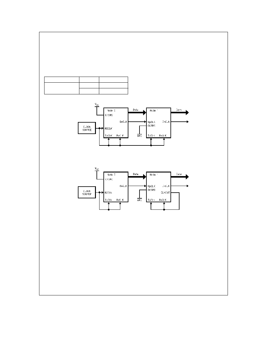
FIGURE 5 1 Recommended for Card-to-Card Connections Over QuickRing
RGCLK on the CKSRC node is driven by the local host clock that drives RxCLK and TxCLK
TL F 11928 � 31
FIGURE 5 2 Recommended for Box-to-Box or Card-to-Card Connectors Over QuickRing
CLKOUT is used on all other nodes to drive RxCLK TxCLK and therefore the HOST SYSTEM CLOCK
Note that CLKOUT is not intended to drive large loads and can only sink a few mA If the application requires the ability to
drive other system clocks then add a buffer
QR0001 Resynchronizer Issue
The core of QR0001 operates in the timing domain of the
ring in which it is connected The intent of the QR0001 de-
sign is to allow the timing domain of the client interface to
be independent of the ring clock domain Unfortunately
there is a bug in the first release of QR0001 that affects
both the transmit and receive resynchronizers whose task is
to decouple the clock domains from each other These cir-
cuits fail in such a way that data may be erroneously repli-
cated or deleted as it crosses between the ring clock do-
main and the client clock domains The failure occurs be-
cause of metastable states in the logic that controls these
resynchronizer blocks
The transmit resynchronizer is susceptible to metastability
whenever the delay between CKOUT and TxCLK falls within
a range which we can call the window of metastability or the
danger window
Likewise the receive resynchronizer may experience me-
tastability and data stream corruption if the delay of RxCLK
from CKOUT falls within its window of metastability
The following two inequalities identify the window of metast-
ability within which metastability and data stream corruption
is possible
23

5 0 Clock Signals
(Continued)
T
COtoTxCmin
k
T
TxMETA
k
T
COtoTxCmax
TL F 11928 � 33
T
COtoRxCmin
k
T
RxMETA
k
T
COtoRxCmax
TL F 11928 � 34
In general the only way to guarantee that TxCLK and
RxCLK never violate the metastability window is to (1) de-
rive TxCLK and RxCLK from CKOUT or from the same
source from which CKOUT is derived and (2) fix the delay
of TxCLK and RxCLK safely outside the window
TL F 11928 � 35
Design your circuit so as to avoid the danger window The
size and position of this window is as specified in the follow-
ing table
T
META
(ns)
Min
Max
Width
T
COtoTxC
b
11
b
7
4
T
COtoRxC
b
1
3
4
Why Falling Edges Blocks within the QR0001 device oper-
ate using two-phase logic In general half of the internal
latches are transparent during the clock-high time and the
other half are transparent during clock-low time It just so
happens that all of the latches involved in this bug are trans-
parent during clock-high time The bug represents a failure
to decisively resolve a logic value to be true or false as
those latches close
on the falling edges of their respective
clocks
What about frequency and duty cycle
The window of me-
tastability is fixed by chip-internal combinatorial delay paths
whose values are independent of the clock frequency and
duty cycle
What are the symptoms It would be extremely rare for any
single symbol to be corrupted However the symbol
stream
will be corrupted as individual symbols or groups of sym-
bols may be randomly dropped or duplicated
What circuits do I need
If you are deriving RxCLK and
TxCLK from a buffered version of CKOUT you are probably
already safe Just analyze your own circuit to make sure that
TxCLK and RxCLK fall
outside the danger window
Multiple Clock Sources to Reduce Ring Jitter on
QR0001
Testing shows rings with more than 4 nodes accumulate
excessive jitter on the ring clock which inhibits maximum
frequency operation One method to stop jitter accumula-
tion and improve frequency performance on large rings is
to provide multiple clocks sources Using several nodes on
all nodes as clock sources reduces accumulated ring jitter
Using multiple clock sources however does increase ring
latency the next QuickRing device (QR1001) is being de-
signed so that only one clock source will be required
A 10 node ring was tested using 3 clock sources It allowed
the ring to operate at full speed (33 MHz) To make a node a
clock source the ``CKSRC'' input pin should be asserted
and the clock should be connected to the ``RGCLK'' pin
Note that all ``RGCLK'' pins in the Ring (Clock Source
Nodes) MUST be exactly the same frequency however
phase relationship is not an issue This necessitates one
master clock source distributed to each QuickRing Clock
Source node figure below ``CKSRC'' asserted activates the
elasticity buffer at the Upstream port This buffer adds 3
clock cycles delay to every symbol that arrives at the port
including vouchers and tickets
Multiple Clock Source Nodes
TL F 11928 � 36
6 0 ABORT Signal
The ABORT signal is an output of the QR0001 Any one of
the following events can cause the ABORT signal to be
asserted
EDC error Although ABORT signal pin is asserted ring
abort
symbol
may
not
propagate
around
entire
QuickRing
Illegal sequence detected on the QuickRing (Refer to
following ring interface sections ) Ring abort symbol
propagates around QuickRing
Node ID detected greater than maximum number of
nodes in the ring Ring abort symbol propagates around
QuickRing
Received an Abort symbol from the upstream port
24

7 0 Bridges
In a single QuickRing ring the maximum number of nodes is
sixteen Within a ring the PIPE signal will most probably be
asserted for ease of interfacing to the QR0001 In a multiple
QuickRing topology the individual rings may be connected
together through bridges The system may implement a very
basic bridge or an intelligent bridge
For a basic bridge implementation two QR0001 controllers
can be directiy connected through their client ports provid-
ing a bridge between two rings The PIPE signal should be
negated in bridge operation so that the Rx and Tx port tim-
ing will be identical Also the TxOK signal is connected to
the RxSTALL signal QR0001 timing characteristics will sup-
port bridging However an external flip-flop may be used to
achieve additional setup and hold time margins For more
sophisticated bridges external logic can implement a added
layer of protocol
The HOP fields are used with respect to bridges when im-
plementing multi-ring topologies The HOP fields may be
used as desired in a single ring topology (i e To distinguish
various data streams ) Refer to Client Interface Field Defini-
tions sections for more information
8 0 Little Big Endian Issues
This QR0001 datasheet uses strict little-endian labeling
conventions to indicate bit positions The device itself is nei-
ther big-endian nor little-endian No assumption is made in
QR0001 about the relative significance of bytes within any
payload symbol
For reference
Big Endian MSB(yte) of the information (data address) is
stored at the least significant address location
Little Endian LSB(yte) of the information (data address) is
stored at the least significant address location
Table 8 0 contains Big Little Endian formats
TABLE 8 0 Big Little Endian
Big Endian
MSB(it)
LSB(it)
Bit 0
Bit 31
0 7
8 15
16 23
24 31
MSB(yte)
LSB(yte)
Byte 0
Byte 1
Byte 2
Byte 3
Address
Address
Address
Address
(n)
(n
a
1)
(n
a
2)
(n
a
3)
Little Endian
MSB(it)
LSB(it)
Bit 31
Bit 0
31 24
23 16
15 8
7 0
MSB(yte)
LSB(yte)
Byte 3
Byte 2
Byte 1
Byte 0
Address
Address
Address
Address
(n
a
3)
(n
a
2)
(n
a
1)
(n)
9 0 Reset and Initialization
9 1 Reset
The controller must be reset after power up RESET can be
released from each node in any order but only after all
nodes are simultaneously in the reset state (for the time
period of the reset pulse width tRSPW timing parameter
82) External logic should assert RESET to all nodes on
the ring during system power up or when ABORT is assert-
ed The release of RESET to node 0 will begin the initializa-
tion process The ring initialization proceeds to completition
only after RESET has been released to all nodes
The first 2 non-null symbols that appear at the receive port
are the node ID number and the largest ID on the ring The
type associated with this information will indicate a non-null
type also These values will be present for one clock cycle
The information can be later retrieved by reading the Diag-
nostics Register through the RxNBL and RxSEL at any time
later
TABLE 9 1 RxS 31 0
31
28
27
0
Node ID
1 1 1 1
1
Max ID
1 1 1 1
1
9 2 Node 0 Selection and Initialization
Only one QuickRing controller in a ring can be designated
as Node 0 (NODE0 asserted) For all other controllers on
the ring NODE0 must be negated Once the QuickRing has
completed the initialization process the ring is ready for nor-
mal operation During normal operation there are no differ-
ences between node 0 and all other nodes
9 3 Node ID Assignment
As RESET is released to each QuickRing controller each
node receives the node ID of its upstream neighbor on
RxS 31 28
assumes that its own address is node ID
a
1
and passes its new node ID to its downstream neighbor
After initialization the first two non-null symbols that appear
at the receive port indicate to the client interface the node
ID number of the controller and the largest ID number on
the ring This information can be used to configure the client
interface
The node ID (Node ID) and largest node ID in the system
(MaxID) can be read later from the internal diagnostics reg-
ister in the controller
9 4 Sequence for Node 0
1 On release of RESET by all nodes the controller with
the NODE0 signal asserted assigns itself to be node 0
2 Node 0 then begins to transmit a stream of identical
symbols at the down stream port whose high order four
bits are 0 0 0 0
whose frame bit is 1 and whose type
field is 0 1
3 The first downstream node to receive this symbol incre-
ments the value to 0 0 0 1
becomes node 1
4 then the node forwards the symbol containing a value
of 1 The type field and frame bit are not changed
5 Each node in turn increments the value and takes on its
own unique node ID
6 When the node 0 receives the symbol at its up stream
port the value of the symbol is the largest ID number in
the ring
7 Node 0 stores this value and forwards it around the
ring but with the type field changed to 1 0
This noti-
fies all other nodes the total number of nodes in the
ring
8 All nodes forward this symbol stream unmodified
25

9 0 Reset and Initialization
(Continued)
9 Once this symbol stream completes its route around
the ring node 0 begins to transmit null symbols whose
frame bits are reset to 0
10 As soon as each node including node 0 detects an up
stream symbol with the frame bit equal to zero its ini-
tialization sequence is completed and it may begin to
transmit vouchers tickets and packets
11 During this sequence the controller forwards the node
ID and eventually the MaxID on the ring to the receive
port
9 5 Sequence for All Other Nodes on the Ring
1 While RESET remains asserted all other nodes (other
then node 0) transmit all ones at the down stream port
2 Release of RESET from a node causes that node to be-
gin monitoring its up stream port While the up stream
type field is 1 1
the node transmits all 1's at the down
stream port
3 When the upstream type field changes to 0 1
the ac-
companying symbol field is interpreted as the node ID of
the upstream neighbor
4 The node increments the symbol field value stores the
new value internally and then forwards the incremental
value including the new
0 1
type code at its down
stream port The stored value becomes the local node
ID This node ID number is propagated to the node's
receive port so the client interface can learn its ID num-
ber
5 Some time later a new stream of symbols arrives at the
up stream port accompanied by the type code 1 0 The
value of this symbol is stored internally and represents
the numerically greatest node ID residing on the ring
The node forwards this symbol stream to its down
stream port This value is also forwarded to the receive
port so the client can learn the number of nodes on the
ring
6 Throughout this sequence the node transmits symbols
with the frame bit set to 1 Eventually a stream of null
symbols is received at the up stream port with the frame
bit reset to 0 As soon as this symbol is forwarded to the
down stream port the node may commence normal ring
operation If at any point there is a node ID detected
whose value is greater than the greatest ID residing on
the ring an abort symbol is sent and it is considered as a
failure For the client interface the first 2 non-null sym-
bols that appear at the receive port are the node ID num-
ber and the largest ID on the ring
10 0 QR0001 Operation Flow
10 1 Ring Traffic Flow Priorities for
DnSS Port Transmission
After the initialization process is complete all nodes on the
QuickRing are ready to transfer packets on the ring Data
streams can be queued de-queued into from the QR0001
through the Client Interface on all nodes As traffic builds on
the ring the QR0001 prioritizes the information flow through
the node that goes onto the ring Following is the list in
descending order of the paths inside the QR0001 that pro-
cess information to be sent out onto the ring through the
downstream (DnSS) port Refer to the QR0001 block dia-
gram
1 The highest priority is given to tickets vouchers to from
other nodes This QR0001 is simply forwarding the ac-
cess symbols on the ring that are destined for other
nodes
2 LB Target Handler Sends out low bandwidth tickets gen-
erated by this node (Includes voucher rejects when ex-
ceeding storage capacity )
3 Target Handler Sends out normal tickets generated by
this node (Includes voucher rejects when exceeding
storage capacity )
4 Local sourced vouchers launched by this node
LB FIFO Generates a voucher when the LBW symbol gets
to the head of the FIFO
X or Y FIFO Generates a voucher as soon as the first sym-
bol is loaded into the FIFO Also generates another vouch-
er as soon as the 21st symbol (associated with the same
head) is loaded into the FIFO Further continues to gener-
ate a voucher for each packet (maximum bundle of 20 sym-
bols)
5 Ring FIFO This QR0001 is forwarding data destined to
other nodes
6 Sends out locally generated packets from this node's X
Y or LB FIFO At the beginning of each packet the traf-
fic flow priorities are checked (The source (X Y or LB)
FIFO can transmit when the Ring FIFO has at least 28
empty positions Locally sourced packets will be held un-
til the Ring FIRO has no more than 12 data symbols )
10 2 Inside the Source Node (Device Transmitting Data)
At the source node as soon as QR0001 latches a head and
a payload symbol in the X or Y FIFO it sends a voucher to
the target node The source node waits until the target node
sends a ticket back before transmitting a packet During this
time the client interface can write payloads into the control-
ler
When QR0001 detects that a single packet will not be
enough to transmit all data in FIFO X or Y another voucher
is sent to the target node Additional vouchers are sent as
soon as the controller deems it necessary to complete the
transmission This action is intended to hide the latency be-
tween the transmission of vouchers and the receipt of tick-
ets A maximum of 7 (3X 3Y and 1 LB) vouchers can be
outstanding from the source node Vouchers have higher
priority than payloads and they can be launched interleaved
in current outgoing packets
At the source node only when a ticket is received is a pack-
et sent A packet is formed by 1 head and anywhere from 1
to 20 payload symbols The largest packet is 21 symbols 1
head symbol and 20 payload symbols The last payload
symbol of a packet is always identified as a tail This is
encoded in the type field
The QuickRing controller does not wait for any specific
number of data symbols to send a packet If the client inter-
face is slow in writing data at the transmit port QR0001
could send packets with less than 21 symbols The same
will occur in transmissions where the total number of pay-
loads is not a multiple of 20 The QuickRing controller is
designed to transmit the data in the transmit pipeline as
soon as possible
10 3 Summary of Source Node Actions
QR0001 sends a voucher from the source node to the tar-
get node as soon as it has at least one payload to transmit
(In the X or Y FIFOs )
26
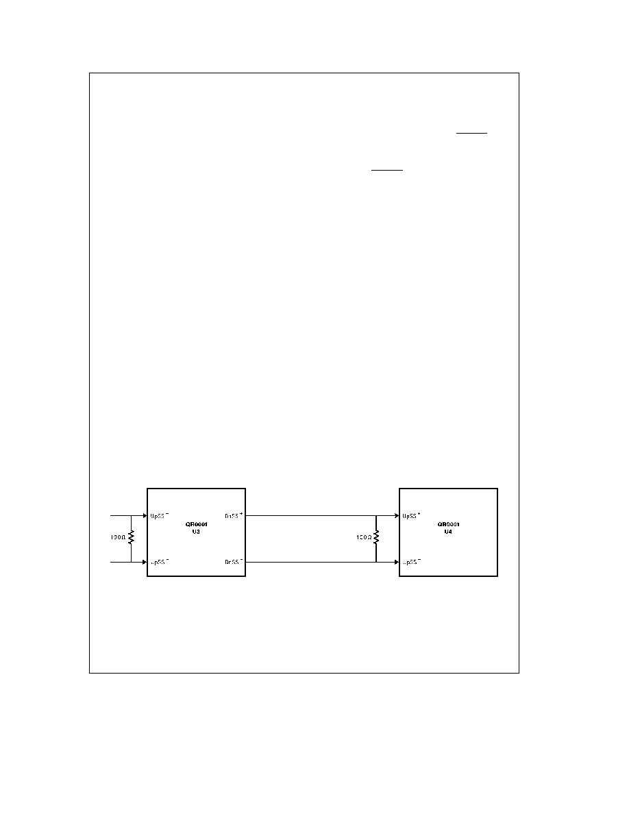
10 0 QR0001 Operation Flow
(Continued)
QR0001 sends an additional voucher as soon as it identifies
that one packet is not going to be enough to transmit all the
data in the transmit pipeline
No packet is sent until a ticket is received This includes low
bandwidth packets
QR0001 does not wait for data therefore packets could
vary in size
The largest and most efficient packet is one formed by 1
head symbol and 20 payload symbols 21 symbols in all
Low Bandwidth packets are 1 head and 1 payload symbol
The client interface must stop writing data at the transmit
port within 20 non-null symbols after TxOK negates The
count is reset if TxOK asserts again
10 4 Inside the Target Node
At the
target node if the receiving controller has space for
one packet in the Target FIFO it will send a ticket immedi-
ately to the source node in response to a voucher A
QR0001 Target FIFO has space for 3 normal packets and 6
low bandwidth packets therefore the controller can have
only 3 outstanding normal tickets and 6 outstanding low
bandwidth tickets If all tickets have been given the receiv-
ing QR0001 will queue incoming vouchers in one of two
special buffers called Target Handler and LB Target Han-
dler The Target Handler can store 30 vouchers and the LB
Target Handler can store 10 vouchers for low bandwidth
transmission
At the
target node a new ticket is released as soon as a
packet has exited the Target FIFO to the Rx Resynchroniz-
er This is determined internally by matching the tickets giv-
en and the tails exiting the target FIFO
If the target node cannot return a ticket or store the voucher
to be handled later it will return a voucher rejected to the
source node (The Source will sink the voucher and the
node will then re-send the voucher after 100 clock cycles )
10 5 Summary of Target Node Actions
The target FIFO can handle 3 normal packets and 6 low
bandwidth packets Therefore only 3 normal tickets and 6
LB tickets can be outstanding at one time
QR0001 can store 30 normal vouchers and 10 LB vouchers
before returning a voucher
reject to the source node
The Head Stripper will remove the head of all packets be-
fore entering the Target FIFO unless there is a change in
stream (new head)
Data may arrive at the Rx Port on every tick of the clock
unless the client stops the flow through the RxSTALL input
RxET can be used to monitor the kind of data entering the
receive pipeline up to 20 symbols before it appears at the
receive port When the Rx pipeline is free flowing in the
unblocked pipe (RxSTALL is negated) RxET will indicate
the Type
1 Three clock cycles early the symbols (RxS) in the pipe-
lined timing and
2 Two clock cycles early the symbols (RxS) in the non-
pipelined timing
11 0 Board Considerations
11 1 Upstream Port Signal Termination
The ring interface upstream port signals UpSS 5 0
and
UpCLK need external termination The termination should
be a 100X resistor between the differential signal pair The
resistor should be placed as close to the upstream port pins
as possible Minimum parasitic inductance and capacitance
is desirable Surface mount chip resistors with
g
1% toler-
ance are recommended See
Figure 11 1
11 2 QuickRing Physical Layer Details
The QuickRing 180 MHz data signals dictate special care
for the physical layer design and layout The use of LVDS
(Low Voltage Differential Signals) enables the very high fre-
quency operation The LVDS also eases design because
the differential signals are forgiving to certain impedance
discontinuities in the signal path If the discontinuities are at
the same electrical distance and have the same magnitude
they will not distort the differential signal Each single ended
signal may appear to have reflections but if the differential
pair has the same minor reflections then the differential
signal will not be affected The skew between the pairs and
inside the pairs is a critical design criteria These are the
basic guidelines for transporting the ring signals
The skew between pairs and between single ended signals
inside a pair is critical First the skew between signal pairs
The 350 MBaud signals only provide a bit width of about
TL F 11928 � 26
FIGURE 11 1 Termination between the Differential Signal pair
27

11 0 Board Considerations
(Continued)
2 86 ns The QuickRing UpPort needs 2 36 ns of this bit
width (including transitions) to successfully sample the val-
ue for each sub-symbol This allows for a total skew budget
of 0 5 ns The interconnect between DnPort and UpPort
should be limited to 350 ps This provides 150 ps skew mar-
gin The 350 ps can be divided between PCB traces con-
nectors headers cables and all other media used in the
signal path
The skew within a pair needs to be controlled because of
the EMI considerations The simultaneous and opposite
transitions on paths within a pair create equal and opposing
electromagnetic fields These EMF the source of EMI
serve to cancel each other thereby reducing EMI The skew
within a pair should be controlled so that the single ended
EMF remain temporally and spatially relevant for the cancel-
ing affect
The length of node interconnects is not critical to the opera-
tion of QuickRing until it degrades signal integrity Nodes in
a ring can have different length interconnects The maxi-
mum length of the interconnect depends on two qualities of
the interconnect transition time degradation and amplitude
antenuation Any extension in transition time due to the high
frequency filter affect of the interconnect takes away from
the skew budget The trade offs between the skew and tran-
sition time degradation must be balanced to allow for the
correct amount of sample time for the UpPort
The signal attenuation affects the differential signal ampli-
tude at the receiver input The receiver requires a differen-
tial voltage of at least 100 mV to guarantee a state The
receiver actually is more sensitive than that under typical
operating conditions but due to power supply and tempera-
ture variations and test limitations this is the data sheet
specification As long as the differential voltage is guaran-
teed to be at least 150 mV and all the skew budget specifi-
cations are met the receiver will operate correctly with ade-
quate noise margin
12 0 Power and Decoupling Issues
12 1 Power Issues
The QR0001 device internally has Four distinct Power re-
gions These regions are labeled (Refer to
Figure 12 3 )
1 Logic Power Pins
(V
CC
4 5 12 13 GND 3 15 18 19 28 29)
2 Client Receive Port Output Power Pins
(V
CC
6 7 8 9 10 11 GND 20 21 22 23 24 25 26 27)
3 LVDS Power Pins
(V
CC
1 3 GND 1 2 4 5 6 7 8 10 11 12 13 14 16 17)
4 PLL and Delay Element Power Pins
(V
CC
2 GND 9)
It is currently recommended that the PC Board have sepa-
rate GND and V
CC
planes Also Power Region 2 should
have some additional isolation from the power plane Com-
plete isolation is not required The isolation aids in limiting
the Receive Port current spikes to the remaining plane Re-
fer to
Figure 12 1
12 2 Decoupling Issues
lt is currently recommended that capacitors be placed local-
ly on all four corners of the device to provide an even filter-
ing Capacitors should also be placed close to power region
2 to provide additional noise filtering Refer to
Figure 12 1
Two capacitors should be placed in parallel to get high and
low frequency filtering along each side However each ca-
pacitor should have a via directiy to the V
CC
and Ground
planes
For power region 4 (PLL and Delay Element Power Pin) two
decoupling capacitors should be placed as close to the pins
as possible (between V
CC2
and GND9) A trace from the pin
directly to the capacitors is recommended and separate
vias to ground plane for each capacitor Refer to
Figure
12 1
TL F 11928 � 28
FIGURE 12 1 QR0001 Power Region Isolation
28

12 0 Power and Decoupling Issues
(Continued)
Following is a List of PCB Recommendations
1 Use one ground plane and at least one V
CC
plane
2 Use a range of decoupling capacitors values These de-
coupling caps should be high Q factor chip capacitors
(chip caps have little parasitic inductance) The differing
QR port frequencies require decoupling over a range of
frequencies The decoupling caps should not share vias
to the ground plane as this would defeat the noise sup-
pression across the desired frequency range
3 Decoupling caps should be placed as close to the device
power pins as possible Extreme care should be taken
placing the Power Region 4 de-couple caps directly on
the power pins These decoupling caps are recommend-
ed as 0 001 mF and 0 01 mF The caps at the RxPort
(region 2) are recommended to be 2 2 mF 1-1 0 mF 1-
0 1 mF 2-0 01 mF These caps should be used as noise
barriers between this region and the high frequency ring
port region Power region (3 and 1 combined) should
have 2-0 1 mF 2-0 01 mF and 680 pF close to the power
pins
4 Care should be taken for ensuring RGCLK TxCLK and
RxCLK have clean transitions and no reflections or ring-
ing Transmission line design techniques must be used
As a rule of thumb if the signal path electrical length
(propagation delay time) is greater than 0 125 times the
clock transition time the line should be terminated
29
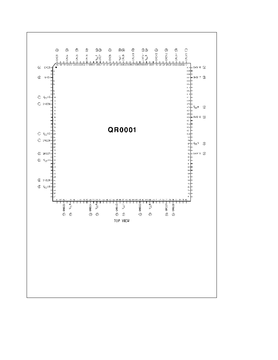
12 0 Power and Decoupling Issues
(Continued)
TL F 11928 � 29
FIGURE 12 3 Power and Ground Regions
30

13 0 DC Electrical Characteristics
PARAMETRICS DISCLAIMER
The current AC and DC specifications contained in this
document are a combination of target design specifica-
tions limited sampled electrical data and some charac-
terization data Currently this information does not rep-
resent all actual guaranteed test timing parameters
Guaranteed specifications will be provided after full de-
vice characterization For more specific information re-
gards DC and AC parameters contact National Semi-
conductor
Absolute Maximum Ratings
DC Supply Voltage (V
CC
)
b
0 5V to
a
7 0V
DC Input Voltage (V
IN
)
b
0 5V to V
CC
a
0 5V
Storage Temperature Range (T
STG
)
b
55 C to
a
l50 C
Power Dissipation (PD)
2 2W
ESD Rating
2000V
Recommended Operating
Conditions
Supply Voltage V
CC
4 5V to 5 5V
Operating Free Air Temperature
0 C to 70 C
DC TTL Specifications Client Ports
T
A
e
0 C to
a
70 C V
CC
e
5V
a
10% unless otherwise specified
Symbol
Parameter
Conditions
Min
Max
Units
V
IH
Minimum High Level Input Voltage
(Note A)
2 0
V
V
IL
Maximum Low Level Input Voltage
(Note A)
0 8
V
V
OH
Minimum High Level Output Voltage
I
OH
e b
400 uA (Note A)
2 4
V
V
OL
Maximum Low Level Output
I
OL
e
1 6 mA (Note A)
0 4
V
Voltage
I
OL
e
8 mA (Note B)
0 4
I
I
Input Leakage Current
V
IN
e
V
CC
(Note A)
b
1 0
1 0
mA
I
IN
Input High Current
V
IN
e
2 0V (Note A)
1 0
mA
I
IL
Input Low Current
V
IN
e
0 8V (Note A)
b
1 0
mA
I
DD
Supply Current
(Note A)
450
mA
I
CC
Average Operating Supply Current
RESET RxSTALL RxOE
e
3 5V
Other CLIENT INPUTS
e
0 4V
200
mA
(Note A)
I
OZ
Maximum TRI-STATE Output
RxOE
e
2V (Note A)
b
10
10
mA
Leakage Current
DC Electrical Characteristics Ring Ports
DC Differential Generator Specifications
T
A
e
0 C to
a
70 C V
CC
e
5V
g
10% unless otherwise specified
Symbol
Parameter
Conditions
Min
Typ
Max
Units
V
OH
Output Voltage High V
OA
and V
OB
R
LOAD
e
100 X (Note B)
V
OL
a
0 3
1 4
1 5
V
V
OL
Output Voltage Low V
OA
and V
OB
(Note B)
0 9
1 0
V
OH
b
0 3
V
V
OD
Differential Output Voltage
(Note B)
g
300
g
400
g
500
mV
D
V
OD
Differential Voltage Change between
(Note B)
0
50
mV
Complimentary Output Stages
D
V
OS
Output Offset Voltage Change between
(Note B)
0
50
mV
Complimentary Output States
DC Receiver Specifications
T
A
e
0 C to
a
70 C V
CC
e
5V
g
10% unless otherwise specified
Symbol
Parameter
Conditions
Min
Typ
Max
Units
V
I
Input Voltage V
IA'
and V
IB'
V
gpd
e
g
900 mV (Note B)
0
3
V
V
TH
Differential High Input Threshold
(Note B)
a
100
mV
V
TL
Differential Low Input Threshold
(Note B)
b
100
mV
Note 1
V
gpd
e
ground potential difference voltage between the generator and receiver
Note A
Limit guaranteed by test program
Note B
Limit based on simulation results
Note C
Limit based on bench characterization
31

13 0 DC Electrical Characteristics
(Continued)
AC Receiver Specifications
T
A
e
0 C to
a
70 C V
CC
e
5V
g
10% unless otherwise specified
Symbol
Parameter
Conditions
Min
Typ
Max
Units
t
pSKEW
Receiver Propagation Delay Skew
Any Two Channels on IC
0
250
ps
(Notes 2 3 B)
t
pwd
Pulse Width Distortion (t
plh
� t
phl
)
One channel at receiver
b
250
a
250
ps
output (Notes 2 3 B)
t
SKEWIN
Single ended skew that can be tolerat-
Measured at 50%
500
ps
ed at receiver inputs
of transition (Notes 2 3 B)
Note 2
These specifications are not tested but verified by design
Note 3
A 300 mV differential signal is used to stimulate the receiver input circuitry
Note B
Limit based on simulation results
AC Differential Generator Specifications
T
A
e
0 C to
a
70 C V
CC
e
5V 10% unless otherwise specified
Symbol
Parameter
Conditions
Min
Typ
Max
Units
t
r
V
OA
and V
OB
Rise Time 20% � 80%
Z
LOAD
e
100 X
150
300
450
ps
t
f
V
OA
and V
OB
Fall Time 80% � 20%
(Note B)
150
300
450
ps
t
SKEW
t Generator Propagation Delay
Any Two Channels on IC (Note B)
200
ps
t
pwd
Pulse Width Distortion (t
plh
� t
phl
)
One Channel Difference
b
200
a
200
ps
between Differential Prop Delays (Note B)
Note A
Limit guaranteed by test program
Note B
Limit based on simulation results
Note C
Limit based on bench characterization
32

14 0 AC Timing Parameters
Parametrlcs Disclaimer
The current AC and DC specifications contained in this doc-
ument are a combination of target design specifications lim-
ited sampled empirical data and some characterization
data Currently this information does not represent all actu-
al guaranteed tested timing parameters Guaranteed specifi-
cations wlll be provided after full device characterization
For more specific information regards DC and AC parame-
ters contact National Semiconductor
AC TTL PARAMETERS
Tx Port Timing
TL F 11928 � 16
Symbol
Description
Min
TYP
Max
Units
1
t
TCKP
Transmit Clock Period
1 f
ns
(Note 1)
(1 f
e
T
50 MHz T
e
20 ns
33 MHz T
e
30 ns (Note C)
2
t
TCKPW
Transmit Clock Pulse Width (fmax
e
50 MHz) (Note C)
1 2f � 20%
1 2f
1 2f
a
ns
(Note 1)
20%
3
t
TDS
Symbol and Type Set up to Clock High
(Note A)
5
3 6
ns
(Note B)
4
4
t
TDH
Symbol and Type Hold Time (Note C)
3
0 7
ns
5
t
TOK
Clock High to TxOK Valid (Note A)
8 7
12
ns
Note 1
This parameter is dependent on clock frequency
Note A
Limit guaranteed by test program
Note B
Limit based on simulation results
Note C
Limit based on bench characterization
33

14 0 AC Timing Parameters
(Continued)
Rx Port Timing
TL F 11928 � 17
Symbol
Description
Min
Typ
Max
Units
50
tRCKP
Receive Clock Period (Note C)
1 f
ns
(Note 1)
51
tTRCKPW
Receive Clock Pulse Width (Note C)
1 2f � 20%
1 2f
1 2f
a
ns
(Note 1)
20%
53
tRSACC
Clock High to Symbol Access Time (Note A)
13
16
ns
54
tRSVAL
Symbol Valid after Clock High (Note C)
3
9 4
ns
55
tRTACC
Clock High to Type Access Time (Note A)
14 2
15
ns
56
tRTVAL
Type Valid after Clock High (Note A)
3
8 8
ns
57
tRSTLS
RxSTALL Set up to Clock Low (Note C)
b
2
b
4
ns
58
tRSTLH
RxSTALL Hold from Clock Low (Note C)
5
2 9
ns
59
tRSHZ
RxOE Negated to Symbol TRI-STATE (Note C)
4 5
8
ns
60
tRSLZ
RxOE Asserted to Symbol Low Z (Note C)
5
9
ns
61
tRNBACC
Clock High to NIBBLE Access Time (Note A)
8 6
19
ns
62
tRNBVAL
NIBBLE Valid after Clock High (Note A)
4
3
ns
63
tRSELNB
SELECT to NIBBLE Valid Access Time (Note A)
14 6
18
ns
64
tRABT
Clock High to ABORT Valid (Note C)
12 5
15
ns
Note A
Limit guaranteed by test program
Note B
Limit based on simulation results
Note C
Limit based on bench characterization
34
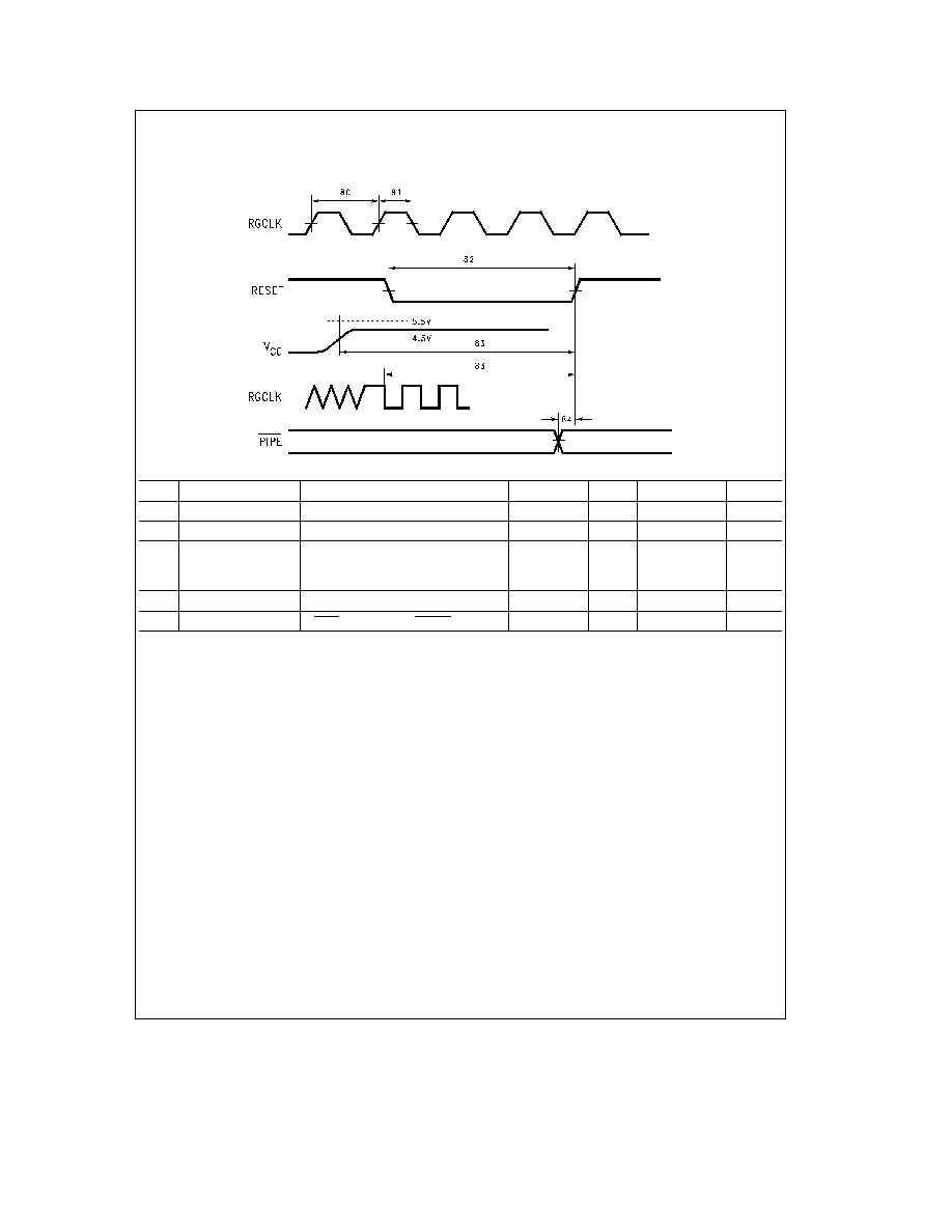
14 0 AC Timing Parameters
(Continued)
Reset and Other Miscellaneous Timing 1
TL F 11928 � 18
Symbol
Description
Min
Typ
Max
Units
80
tRGCKP (Note 1)
RGCLK Clock Period (Note C)
1 f
ns
81
tRGCKPW (Note 1)
RGCLK Clock pulse Width (Note C)
1 2f � 20%
1 2f
1 2f
a
20%
ns
82
tRSPW (Note 1)
RESET Pulse Width (Note C)
50 MHz
230
100
ns
33 MHz
320
150
ns
83
tPLLS
Phase Lock Loop Set (Note B)
3
ms
84
tPIPES
PIPE Set Up Time to RESET (Note C)
0
ns
Note 1
This parameter is dependent on clock frequency
At 50 MHz i e tRCKP
e
tRGCKP
e
tTCKP
e
20 ns Otherwise tRSPW
e
tRCKP
a
7(tRGCKP)
a
tTCKP
a
50 ns
At one node otherwise tPLLS
e
1 5 (node number
a
1) ms
Note A
Limit guaranteed by test program
Note B
Limit based on simulation results
Note C
Limit based on bench characterization
35
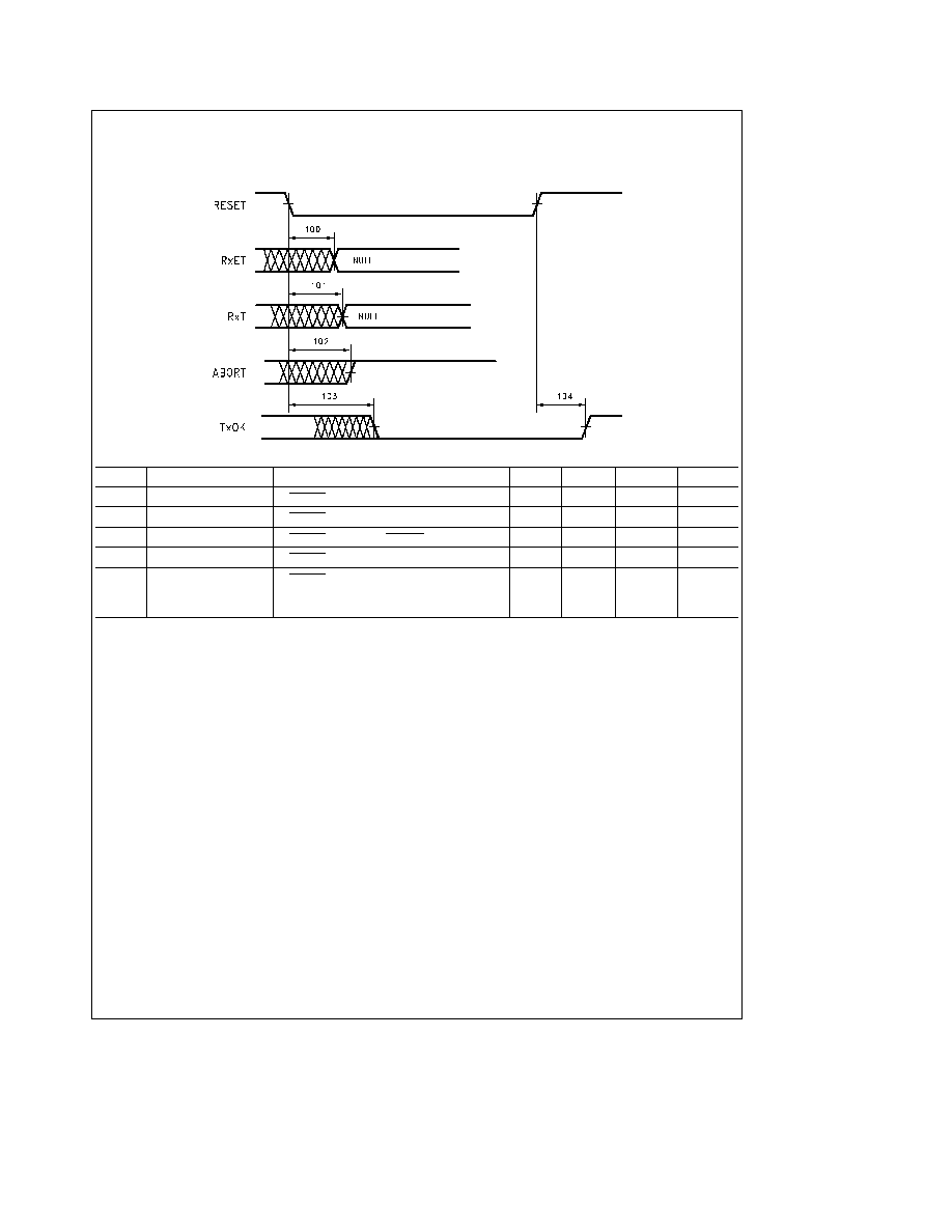
14 0 AC Timing Parameters
(Continued)
Reset and Other Miscellaneous Timing 2
TL F 11928 � 19
Symbol
Description
Min
Typ
Max
Units
100
tRSET
RESET Asserted to RxETValid (Note C)
25
55
ns
101
tRST
RESET Asserted to RxT Valid (Note C)
22
55
ns
102
tRSABT
RESET Asserted to ABORT Valid (Note C)
10 2
35
ns
103
tRSTXOKN
RESET Asserted to TxOK Low (Note C)
14 6
35
ns
104
tRSTXOK (Note 1)
RESET Negated to TxOK High
50 MHz (Note C)
150
191
ns
33 MHz (Note A)
220
282
ns
Note 1
This parameter is dependent on clock frequency
At tRCKP
e
20 ns Otherwise tRSET
e
tRST
e
2tRCKP
a
15 ns
At 50 MHz i e tRCKP
e
tRGCKP
e
tTCKP
e
20 ns Otherwise tRSTXOKmax
e
tRCKP
a
7tRGCKP
a
tTCKP
a
tTOK
Note A
Limit guaranteed by test program
Note B
Limit based on simulation results
Note C
Limit based on bench characterization
36

15 0 Connection Diagram
TL F 11928 � 20
Order Number QR0001-33VUL
37

16 0 Glossary
bridge
mode
The
ability
to
directly
connect
one
QuickRing client port to another QuickRing client port This
will provide a hop path from one ring structure to another
(PIPE signal is negated )
hop fields
The ring packet header has 5 fields allocated
to address to different rings If the fields are not used to hop
rings they can be used to identify separate data streams
This allows up to 2
20
individually identified data streams
hop path
The means of moving from one QuickRing to
another through a bridge connection Hop fields in the head-
er symbol provide the addressing to achieve the routing
initialization
A user transparent process that begins upon
reset release by all nodes During initialization nodes are
assigned node ID numbers then the total number of nodes
on the ring is distributed to each node The node address
and total number of nodes is made available to the client
Reservation and packet transmissions may begin immedi-
ately following
Node0
Node 0 is determined by the Node0 pin being as-
serted Node 0 governs the initialization process
ring of rings
The result of connecting multiple rings to-
gether Up to 5 QuickRings can be traversed by a packet
because there are 5 hop fields in the header
symbol
The ring transmission basic unit on the ring Each
symbol consists of 42 bits 2 type bits 1 frame bit 32 data
bits and 7 bits of error detection code At the client ports a
symbol is a 32-bit value on RxS 31 0 or TxS 31 0
voucher
On the ring vouchers are sent by source nodes
to obtain permission to launch packets of client generated
payload symbols
ticket
On the ring tickets are returned by target nodes in
response to vouchers They indicate that the target has re-
served FIFO space for one packet
packets
On the ring packets are limited to a size of 21
Each packet at least consists of 1 head symbol and 1 tail
symbol last symbol
Null
Null is the encoding on the Type fields which indi-
cates to ignore the associated symbol
17 0 Revision Notes
Following is a list of some of the changes that have been
made between this version of the datasheet and the
December 1993 version This is not a complete list of the
changes
Change
Section
Maximum Data Transfer Rate
Front page
Client receive port operation
3 5 1
EDC error and client ``abort'' pin functionality
3 16
Resynchronizer issue
5 0
Multiple clock sources and ring with many nodes
5 0
Power and decoupling recommendations
12 0
38

39

QR0001
QuickRing
Data
Stream
Controller
Physical Dimensions
inches (millimeters)
160-Lead (28mm x 28mm) Molded Plastic
Quad Flatpak JEDEC
NS Package Number VUL160A
QuickRing
TM
is a trademark of Apple Computer Incorporated
LIFE SUPPORT POLICY
NATIONAL'S PRODUCTS ARE NOT AUTHORIZED FOR USE AS CRITICAL COMPONENTS IN LIFE SUPPORT
DEVICES OR SYSTEMS WITHOUT THE EXPRESS WRITTEN APPROVAL OF THE PRESIDENT OF NATIONAL
SEMICONDUCTOR CORPORATION As used herein
1 Life support devices or systems are devices or
2 A critical component is any component of a life
systems which (a) are intended for surgical implant
support device or system whose failure to perform can
into the body or (b) support or sustain life and whose
be reasonably expected to cause the failure of the life
failure to perform when properly used in accordance
support device or system or to affect its safety or
with instructions for use provided in the labeling can
effectiveness
be reasonably expected to result in a significant injury
to the user
National Semiconductor
National Semiconductor
National Semiconductor
National Semiconductor
National Semiconductores
National Semiconductor
Corporation
GmbH
Japan Ltd
Hong Kong Ltd
Do Brazil Ltda
(Australia) Pty Ltd
2900 Semiconductor Drive
Livry-Gargan-Str 10
Sumitomo Chemical
13th Floor Straight Block
Rue Deputado Lacorda Franco
Building 16
P O Box 58090
D-82256 F4urstenfeldbruck
Engineering Center
Ocean Centre 5 Canton Rd
120-3A
Business Park Drive
Santa Clara CA 95052-8090
Germany
Bldg 7F
Tsimshatsui Kowloon
Sao Paulo-SP
Monash Business Park
Tel 1(800) 272-9959
Tel (81-41) 35-0
1-7-1 Nakase Mihama-Ku
Hong Kong
Brazil 05418-000
Nottinghill Melbourne
TWX (910) 339-9240
Telex 527649
Chiba-City
Tel (852) 2737-1600
Tel (55-11) 212-5066
Victoria 3168 Australia
Fax (81-41) 35-1
Ciba Prefecture 261
Fax (852) 2736-9960
Telex 391-1131931 NSBR BR
Tel (3) 558-9999
Tel (043) 299-2300
Fax (55-11) 212-1181
Fax (3) 558-9998
Fax (043) 299-2500
National does not assume any responsibility for use of any circuitry described no circuit patent licenses are implied and National reserves the right at any time without notice to change said circuitry and specifications