NTE1979
Integrated Circuit
Negative 3 Terminal Voltage Regulator,
≠8V, 100mA
Description:
The NTE1979 is a 3≠terminal fixed negative output voltage regulatgor in a TO92 type package
designed for use in power circuits with current capacity up to 100mA. Stabilized fixed output voltage
is obtained from unstable DC input voltage without the use of external components.
Features:
D
No External Components
D
Output Current in Excess of 100mA
D
Built≠In Short≠Circuit Current Limiting
D
Built≠In Thermal Overload Protection
Absolute Maximum Ratings: (T
A
= +25
į
C unless otherwise specified)
Input Voltage, V
I
≠35V
. . . . . . . . . . . . . . . . . . . . . . . . . . . . . . . . . . . . . . . . . . . . . . . . . . . . . . . . . . . . . . . . . .
Power Dissipation (Note 1), P
D
650mW
. . . . . . . . . . . . . . . . . . . . . . . . . . . . . . . . . . . . . . . . . . . . . . . . . . . .
Operating Ambient Temperature Range, T
opr
≠20
į
to +80
į
C
. . . . . . . . . . . . . . . . . . . . . . . . . . . . . . . . . .
Storage Temperature Range, T
stg
≠55
į
to +150
į
C
. . . . . . . . . . . . . . . . . . . . . . . . . . . . . . . . . . . . . . . . . .
Note 1. When T
J
exceeds +150
į
C, the internal circuit cuts off the output.
Electrical Characteristics: (T
A
= +25
į
C, V
I
= ≠14V, I
O
= 40mA, C
i
= 2
Ķ
F, C
o
= 1
Ķ
F unless
otherwise specified)
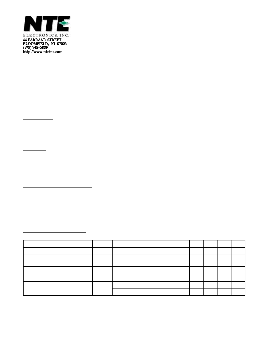
Parameter
Symbol
Test Conditions
Min
Typ
Max
Unit
Output Voltage
V
O
T
J
= +25
į
C
≠7.68
≠8.0
≠8.32
V
Output Voltage Tolerance
V
O
V
I
= ≠11V to ≠23V, I
O
= 1mA to 70mA,
T
J
= 0
į
to +125
į
C
≠7.6
≠
≠8.4
V
Line Regulation
REG
IN
V
I
= ≠10V to ≠24V, T
J
= +25
į
C
≠
≠
160
mV
V
I
= ≠11V to ≠21V, T
J
= +25
į
C
≠
≠
80
mV
Load Regulation
REG
L
I
O
= 1mA to 100mA, T
J
= +25
į
C
≠
15
80
mV
I
O
= 1mA to 40mA, T
J
= +25
į
C
≠
7
40
mA
Note 2. The specified condition T
J
= +25
į
C means that the test should be carried out with the test
time so short (within 10ms) that the drift in characteristic value due to the rise in chip junction
temperature can be ignored.
Electrical Characteristics (Cont'd):
(T
A
= +25
į
C, V
I
= ≠14V, I
O
= 40mA, C
i
= 2
Ķ
F, C
o
= 1
Ķ
F
unless otherwise specified)
Parameter
Symbol
Test Conditions
Min
Typ
Max
Unit
Bias Current
I
BIAS
T
J
= +25
į
C
≠
3
5
mA
Input Bias Current Fluctuation
I
BIAS(IN)
V
I
= ≠11V to ≠23V, T
J
= +25
į
C
≠
≠
0.5
mA
I
BIAS(L)
I
O
= 1mA to 40mA, T
J
= +25
į
C
≠
≠
0.1
mA
Output Noise Voltage
V
no
f = 10Hz to 100kHz, T
A
= +25
į
C
≠
52
≠
Ķ
V
Ripple Rejection Ratio
RR
V
I
= ≠11V to ≠21V, f = 120Hz, T
A
= +25
į
C
54
≠
≠
dB
Minimum I/O Voltage Difference
V
DIF(min)
T
J
= +25
į
C
≠
0.8
≠
V
Output Short Circuit Current
I
O(Short)
V
I
= ≠35V, T
J
= +25
į
C
≠
200
≠
mA
Output Voltage Temperature
Coefficient
V
O
/T
A
I
O
= 5mA, T
J
= 0
į
to +125
į
C
≠
≠0.6
≠
mV/
į
C
Note 2. The specified condition T
J
= +25
į
C means that the test should be carried out with the test
time so short (within 10ms) that the drift in characteristic value due to the rise in chip junction
temperature can be ignored.
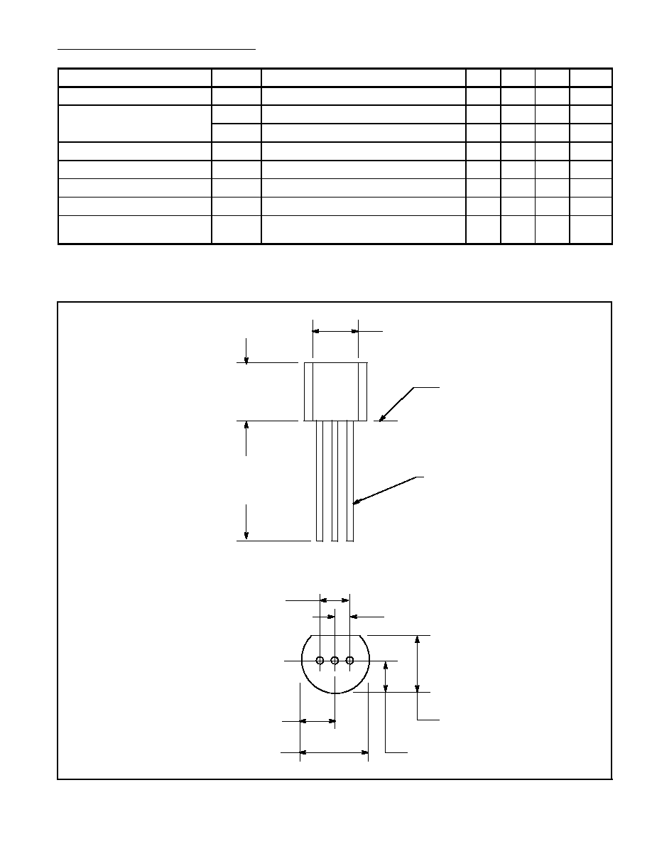
V
OUT
Common
V
IN
.135 (3.45) Min
Seating Plane
.021 (.445) Dia Max
.210
(5.33)
Max
.500
(12.7)
Min
.050 (1.27)
.165 (4.2) Max
.105 (2.67) Max
.100 (2.54)
.105 (2.67) Max
.205 (5.2) Max