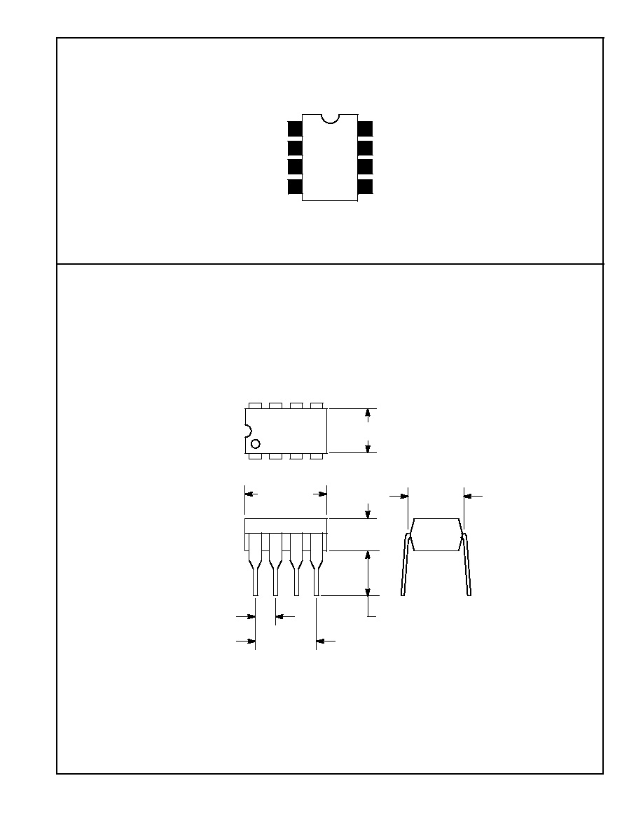
NTE7144
Integrated Circuit
BIMOS Operational Amplifier
w
/MOSFET Input, Bipolar Output
Description:
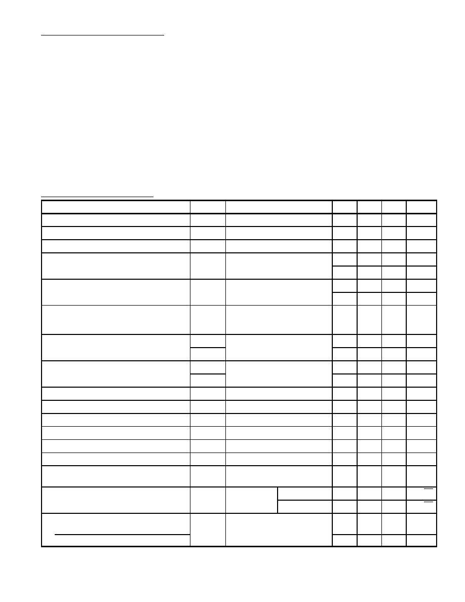
The NTE7144 is an integrated circuit operational amplifier in an 8¡Lead Mini¡DIP type package that
combines the advantages of high¡voltage PMOS transistors with high¡voltage bipolar transistors on
a single monolithic chip. This device features gate¡protected MOSFET (PMOS) transistors in the in-
put circuit to provide very¡high¡input impedance, very¡low¡input current, and high¡speed perfor-
mance. The NTE7144 operates at supply voltages from 4V to 36V (either single or dual supply) and
is internally phase¡compensated to achieve stable operation in unity¡gain follower operation.
The use of PMOS field¡effect transistors in the input stage results in common¡mode input¡voltage
capability down to 0.5V below the negative¡supply terminal, an important attribute for single¡supply
applications. The output stage uses bipolar transistors and includes built¡in protection against dam-
age from load¡terminal short¡circuiting to either supply¡rail or to GND.
Features:
D
MOSFET Input Stage:
Very High Input Impedance
Very Low Input Current
Wide Common¡Mode Input Voltage Range
Output Swing Complements Input Common¡Mode Range
D
Directly Replaces Industry Type 741 in Most Applications
Applications:
D
Ground¡Referenced Single¡Supply Amplifiers in Automobile and Portable Instrumentation
D
Sample and Hold Amplifiers
D
Long¡Duration Timers/Multivibrators (Microseconds ¡ Minutes ¡ Hours)
D
Photocurrent Instrumentation
D
Peak Detectors
D
Active Filters
D
Comparators
D
Interface in 5V TTL Systems and other Low¡Supply Voltage Systems
D
All Standard Operational Amplifier Applications
D
Function Generators
D
Tone Controls
D
Power Supplies
D
Portable Instruments
D
Intrusion Alarm Systems
Absolute Maximum Ratings:
DC Supply Voltage (Between V+ and V¡ Terminals)
36V
. . . . . . . . . . . . . . . . . . . . . . . . . . . . . . . . . . . .
Differential¡Mode Input Voltage
▒
8V
. . . . . . . . . . . . . . . . . . . . . . . . . . . . . . . . . . . . . . . . . . . . . . . . . . . . . .
Common¡Mode DC Input Voltage
(V+ +8V) to (V¡ ¡0.5V)
. . . . . . . . . . . . . . . . . . . . . . . . . . . . . . . . . . .
Input¡Terminal Current
1mA
. . . . . . . . . . . . . . . . . . . . . . . . . . . . . . . . . . . . . . . . . . . . . . . . . . . . . . . . . . . . .
Device Dissipation (Without Heatsink), P
D
630mW
. . . . . . . . . . . . . . . . . . . . . . . . . . . . . . . . . . . . . . . . . .
Derate Linearly Above +55
░
C
6.67mW/
░
C
. . . . . . . . . . . . . . . . . . . . . . . . . . . . . . . . . . . . . . . . . . .
Device Dissipation (With Heatsink), P
D
1W
. . . . . . . . . . . . . . . . . . . . . . . . . . . . . . . . . . . . . . . . . . . . . . . .
Derate Linearly Above +55
░
C
16.7mW/
░
C
. . . . . . . . . . . . . . . . . . . . . . . . . . . . . . . . . . . . . . . . . . .
Operating Temperature Range, T
opr
¡55
░
to +125
░
C
. . . . . . . . . . . . . . . . . . . . . . . . . . . . . . . . . . . . . . . .
Storage Temperature Range, T
stg
¡65
░
to +150
░
C
. . . . . . . . . . . . . . . . . . . . . . . . . . . . . . . . . . . . . . . . . .
Lead Temperature (During Soldering, 1/16" from case, 10sec max), T
L
+265
░
C
. . . . . . . . . . . . . . . . .
Output Short¡Circuit Duration (Note 1)
Unlimited
. . . . . . . . . . . . . . . . . . . . . . . . . . . . . . . . . . . . . . . . . . .
Note 1. Short circuit may be applied to GND or to either supply.
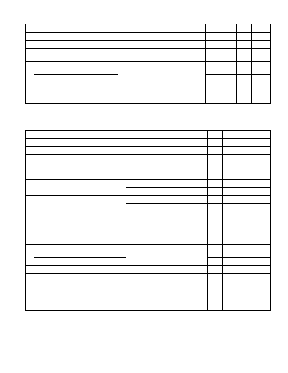
Electrical Characteristics: (T
A
= +25
░
C, V+ = +15V, V¡ = ¡15V unless otherwise specified)
Parameter
Symbol
Test Conditions
Min
Typ
Max
Unit
Input Offset Voltage
|V
IO
|
¡
2
5
mV
Input Offset Current
|I
IO
|
¡
0.5
20
pA
Input Current
I
I
¡
10
40
pA
Large¡Signal Voltage Gain
A
OL
Note 2
20k
100k
¡
V/V
86
100
¡
dB
Common¡Mode Rejection Ratio
CMRR
¡
32
320
╡
V/V
70
90
¡
dB
Common¡Mode Input¡Voltage
Range
V
ICR
¡15
¡15.5
to
+12.5
+12
V
Power Supply Rejection Ratio
V
IO
/
V
¡
100
150
╡
V/V
PSSR
76
80
¡
dB
Maximum Output Voltage
V
OM
+
R
L
= 2k
+12
+13
¡
V
V
OM
¡
¡14
¡14.4
¡
V
Supply Current
I+
¡
4
6
mA
Device Dissipation
P
D
¡
120
180
mW
Input Offset Voltage Temp. Drift
V
IO
/
T
¡
6
¡
╡
A/
░
C
Input Resistance
R
I
¡
1.5
¡
T
Input Capacitance
C
I
¡
4
¡
pF
Output Resistance
R
O
¡
60
¡
Equivalent Wideband Input Noise
Voltage
e
n
BW = 140kHz, R
S
= 1M
¡
48
¡
╡
V
Equivalent Input Noise Voltage
e
n
R
S
= 100
f ¡ 1kHz
¡
40
¡
nV/
Hz
f = 10kHz
¡
12
¡
nV/
Hz
Short¡Circuit Current to Opposite Supply
Source
I
OM
+
¡
40
¡
mA
Sink
I
OM
¡
¡
18
¡
mA
Note 2. V
O
= 26V
P¡P
, +12V, ¡14V and R
L
= 2k
.
Electrical Characteristics (Cont'd): (T
A
= +25
░
C, V+ = +15V, V¡ = ¡15V unless otherwise specified)
Parameter
Symbol
Test Conditions
Min
Typ
Max
Unit
Gain¡Bandwidth Product
f
T
¡
4.5
¡
MHz
Slew Rate
SR
¡
9
¡
V/
╡
s
Sink Current from Pin8 to Pin4 to Swing
Output Low
¡
220
¡
╡
A
Transient Response:
Rise Time
t
r
R
L
= 2k
, C
L
= 100pF
¡
0.08
¡
╡
s
Overshoot
¡
10
¡
%
Setting Time at 10V
P¡P
1mV
t
s
R
L
= 2k
, C
L
= 100pF,
¡
4.5
¡
╡
s
10mV
Voltage Follower
¡
1.4
¡
╡
s
Note 2. V
O
= 26V
P¡P
, +12V, ¡14V and R
L
= 2k
.
Electrical Characteristics: (T
A
= +25
░
C, V+ = +5V, V¡ = ¡5V unless otherwise specified)
Input Offset Voltage
|V
IO
|
¡
2
¡
mV
Input Offset Current
|I
IO
|
¡
0.1
¡
pA
Input Current
I
I
¡
2
¡
pA
Input Resistance
R
I
¡
1
¡
T
Large¡Signal Voltage Gain
A
OL
¡
100k
¡
V/V
¡
100
¡
dB
Common¡Mode Rejection Ratio
CMRR
¡
32
¡
╡
V/V
¡
90
¡
dB
Common¡Mode Input¡Voltage Range
V
ICR
¡
¡0.5
¡
V
¡
+2.6
¡
V
Power Supply Rejection Ratio
V
IO
/
V
¡
100
¡
╡
V/V
PSSR
¡
80
¡
dB
Maximum Output Voltage
V
OM
+
¡
3.0
¡
V
V
OM
¡
¡
0.13
¡
V
Maximum Output Current:
Source
I
OM
+
¡
10
¡
mA
Sink
I
OM
¡
¡
1
¡
mA
Slew Rate
SR
¡
7
¡
V/
╡
s
Gain¡Bandwidth Product
f
T
¡
3.7
¡
MHz
Supply Current
I+
¡
1.6
¡
mA
Device Dissipation
P
D
¡
8
¡
mW
Sink Current from Pin8 to Pin4 to
Swing Output Low
¡
200
¡
╡
A