 | –≠–ª–µ–∫—Ç—Ä–æ–Ω–Ω—ã–π –∫–æ–º–ø–æ–Ω–µ–Ω—Ç: nRF903 | –°–∫–∞—á–∞—Ç—å:  PDF PDF  ZIP ZIP |
PRODUCT SPECIFICATION
Nordic VLSI ASA - Vestre Rosten 81, N-7075 Tiller, Norway - Phone +4772898900 - Fax +4772898989
Revision: 3.1
Qhtr√ √s√"!
December 2002
430MHz-950MHz
Single Chip RF Transceiver
)($785(6
∑
Single chip GFSK multi-channel
transceiver
∑
433MHz, 868MHz and 915MHz
ISM/LPRD-bands compatible
∑
76.8kbit/s data rate
∑
High bandwidth efficiency
∑
Easy 14-bit configuration
∑
Reliable communication due to
superior adjacent channel selectivity
∑
Full output power in all ISM-bands
∑
Few external components required
∑
Standby- and power down-mode
$33/,&$7,216
∑
Alarm and Security Systems
∑
Automotive
∑
Home Automation
∑
Automatic Meter Reading (AMR)
∑
Wireless Handsfree
∑
Remote Control
∑
Surveillance
∑
Wireless Communications
∑
Telemetry
∑
Toys
*(1(5$/ '(6&5,37,21
nRF903 is a true single chip multi-channel UHF transceiver designed to operate in the
unlicensed 433MHz, 868MHz and 915MHz ISM-/LPRD- (Industrial Scientific Medical /
Low Power Radio Device) bands. Multi-channel operation, excellent receiver selectivity and
sensitivity, high bandwidth efficiency and blocking performance make the nRF903 suitable
for wireless links where high reliability is a key requirement.
The device features GFSK (Gaussian Frequency Shift Keying) modulation and demodulation
capability at an effective bit rate of 76.8kbit/s in 153.6kHz channel bandwidths. Transmit
power can be adjusted to a maximum of 10dBm which is available for all frequency bands
and channels. Antenna interface is differential and suited for low cost PCB-antennas. All
necessary configuration data is programmed by a 14-bit configuration word via a Serial
Peripheral Interface (SPI). nRF903 operates from a single +3V DC supply and features power
down- and standby-modes which makes power saving easy and efficient.
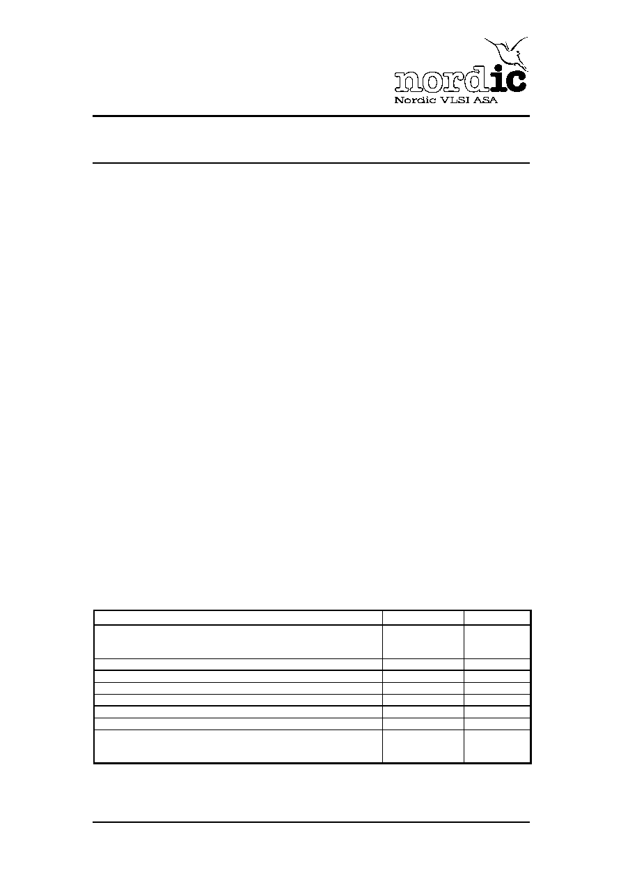
48,&. 5()(5(1&( '$7$
3DUDPHWHU
9DOXH
8QLW
Frequency bands
433.05 - 434.87
868 - 870
902-928
MHz
Datarate
76.8
kbit/s
Sensitivity @ 300
, BR=76.8kbit/s, BER<10
-3
-104
dBm
Modulation
GFSK
Blocking performance (>1 MHz from carrier)
>50
dB
Max. RF output power @ 300
, 3V
10
dBm
Supply voltage
2.7 ≠ 3.3
V
Number of available channels
433.05 - 434.87 MHz
868 - 870 MHz
902-928 MHz
10
7
169
-
Table 1. nRF903 quick reference data.
Q5)
PRODUCT SPECIFICATION
Q5) 6LQJOH &KLS 5) 7UDQVFHLYHU
Nordic VLSI ASA - Vestre Rosten 81, N-7075 Tiller, Norway - Phone +4772898900 - Fax +4772898989
Revision: 3.1
Qhtr√!√s√"!
December 2002
As a primary application, the transceiver is intended for UHF radio equipment in
compliance with the European Telecommunication Standard Institute (ETSI)
specification EN 300 220-1 and the US Federal Communications Commission (FCC)
standard CFR47, part 15.
25'(5,1* ,1)250$7,21
7\SH QXPEHU
'HVFULSWLRQ
9HUVLRQ
nRF903-IC
32 pin TQFP
A
nRF903-EVKIT-433
nRF903-EVKIT-868
nRF903-EVKIT-915
Evaluation kit (2 test PCBs)
Suffix designate frequency band
1.0
1.0
1.0
nRF903-DEMO
Demonstration kit (4 transceiver units)
1.0
Table 2. nRF903 ordering information.
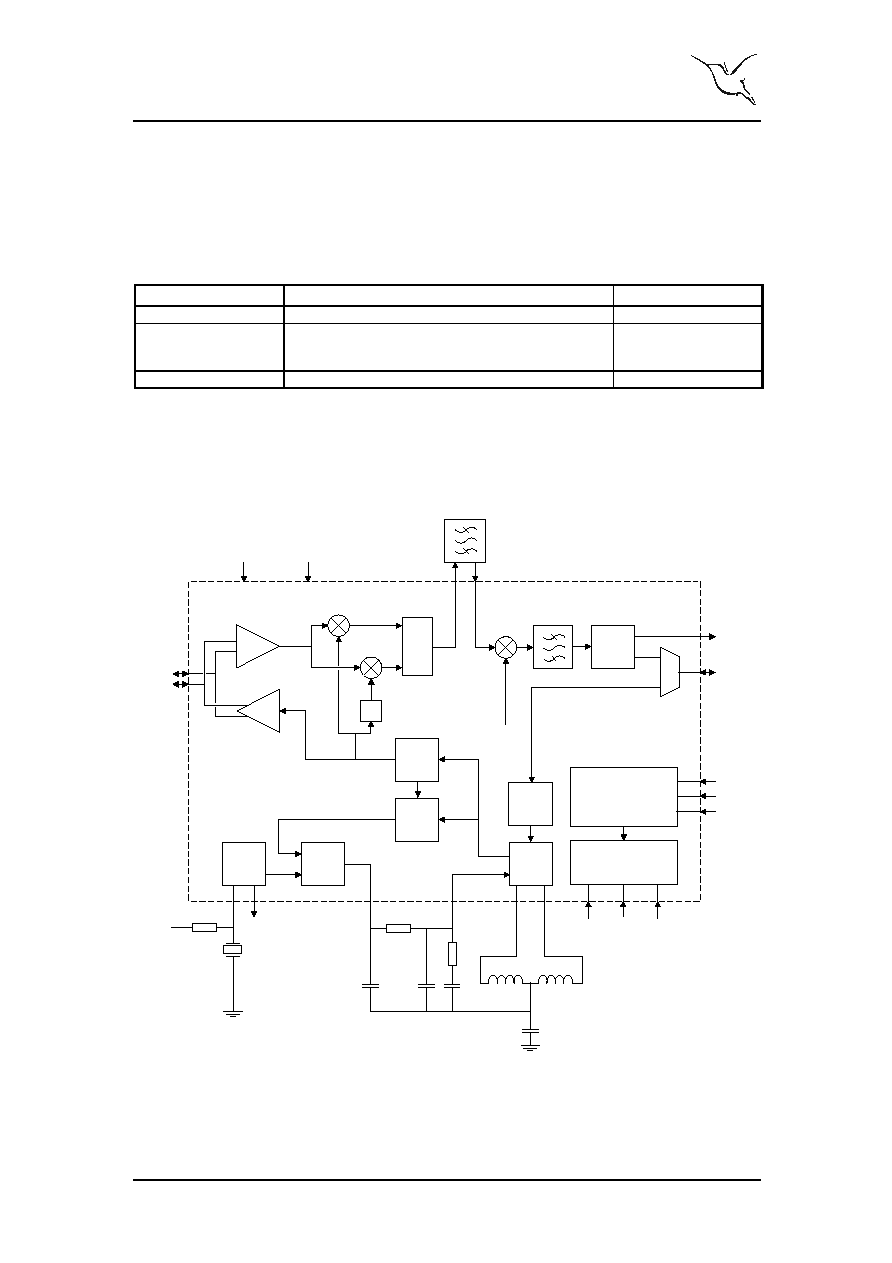
%/2&. ',$*5$0
90
o
po
l
y
p
h
a
s
e
f
ilte
r
LNA
GFSK
demod.
PA
XOSC
VCO
Serial
interface
unit
13
2
4
5
12
10
11
19
28
29
REFERENCE
25
mux
DATA
CS
CFG_CLK
CFG_DATA
PW
R
_
D
W
N
ANT1
ANT2
Dout
Din
IF-filter
C_SENSE
20
T
XEN
26
ST
B
Y
16
CL
K
_
O
U
T
18
f
s
=4*f
IF
FI
L
T
2
FI
L
T
1
22
21
10.7MHz Ceramic filter
LOOP FILTER
C
2
C
1
C
3
R
1
R
2
V
DD
L
2
L
1
C
decoupl
Transceiver control and
configuration register
LF
1
3
LF
2
IN
D
1
IN
D
2
11
.
0
59
2M
H
z
1, 6, 7, 17, 23,
24, 27, 30, 32
VSS
8, 9, 14,
15, 31
VD
D
Q5)
TQFP32
R
3
V
DD
�
GFSK-
modulator
PFD
and
CP
1/M
FREQ
*2
11
.
0
59
2M
H
z
*) The external filter may be replaced with a 10nF capacitor at the expense of receiver performance (see page 18)
Figure 1. nRF903 block diagram with external components.
PRODUCT SPECIFICATION
Q5) 6LQJOH &KLS 5) 7UDQVFHLYHU
Nordic VLSI ASA - Vestre Rosten 81, N-7075 Tiller, Norway - Phone +4772898900 - Fax +4772898989
Revision: 3.1
Qhtr√"√s√"!
December 2002
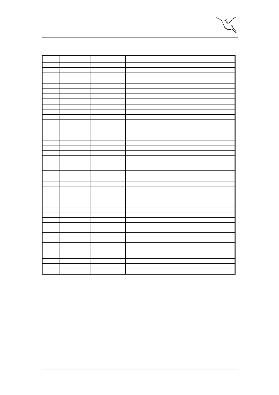
3,1 )81&7,216
3LQ
1DPH
3LQ IXQFWLRQ
'HVFULSWLRQ
1
VSS
Ground
Ground (0V)
2
LF1
Output
Frequency synthesiser PLL loopfilter connection #1
3
LF2
Input
Frequency synthesiser PLL loopfilter connection #2
4
IND1
Input
External inductor for VCO
5
IND2
Input
External inductor for VCO
6
VSS
Ground
Ground (0V)
7
VSS
Ground
Ground (0V)
8
VDD
Power
Power supply (+3.0V DC)
9
VDD
Power
Power supply (+3.0V DC)
10
CFG_CLK
Input
Clock for programming mode
11
CFG_DATA
Input
Serial input for transceiver configuration data
12
CS
Input
Chip select
CS = "0"
transceiver normal operating mode
CS = "1"
transceiver programming mode/test mode
Refer to Table 5. for mode setup
13
XC1
Input
Crystal oscillator input (11.0592MHz)
14
VDD
Power
Power supply (+3.0V DC)
15
VDD
Power
Power supply (+3.0V DC)
16
CLK_OUT
Output
Full swing clock for external microcontroller
Output frequency is set by 2 bits in the configuration word
f
CLK_OUT
=11.0592MHz/
Q, where Q is 1,2,4 or 8
17
VSS
Ground
Ground (0V)
18
C_SENSE
Output
Receiver carrier sense
19
DATA
Bidirectional
Transmitted/received data
20
TXEN
Input
Select transmit/receive mode
TXEN = "0"
Receive mode
TXEN = "1"
Transmit mode
21
FILT2
Input
Input from external 10.7MHz IF filter
22
FILT1
Output
Output to external 10.7MHz IF filter
23
VSS
Ground
Ground (0V)
24
VSS
Ground
Ground (0V)
25
PWR_DWN
Input
Power down mode
Refer to Table 5. for mode setup
26
STBY
Input
Standby mode
Refer to Table 5. for mode setup
27
VSS
Ground
Ground (0V)
28
ANT1
Bidirectional
Antenna terminal
29
ANT2
Bidirectional
Antenna terminal
30
VSS
Ground
Ground (0V)
31
VDD
Power
Power supply (+3.0V DC)
32
VSS
Ground
Ground (0V)
Table 3. nRF903 pin functions.
PRODUCT SPECIFICATION
Q5) 6LQJOH &KLS 5) 7UDQVFHLYHU
Nordic VLSI ASA - Vestre Rosten 81, N-7075 Tiller, Norway - Phone +4772898900 - Fax +4772898989
Revision: 3.1
Qhtr√#√s√"!
December 2002
(/(&75,&$/ 63(&,),&$7,216
Conditions: VDD = +3V DC, VSS
= 0V, T
A
= -40
∞
C to +85
∞
C
6\PERO
3DUDPHWHU FRQGLWLRQ�
0LQ
7\S
0D[ 8QLWV
VDD
Supply voltage
2.7
3
3.3
V
t
Operating temperature range
-40
27
+85
∞
C
I
DD
Total current consumption:
Receive mode : 433MHz
: 868-928MHz
Transmit mode @ -8 dBm RF power : 433MHz
: 868-928MHz
Transmit mode @ 10 dBm RF power : 433MHz
: 868-928MHz
Standby mode
Power-down mode
18.5
22.5
12.5
15.5
24
29.5
600
1
mA
mA
mA
mA
mA
mA
µ
A
µ
A
#CH
Number of available channels with fixed inductor
1)
169
Modulation type
GFSK
f
Frequency deviation
±
19
±
23
±
27
kHz
BR
Bit rate
76.8
kbit/s
P
RF
Max. RF output power @ 300
load
10
dBm
Sensitivity @ 300
, BR=76.8kbit/s, BER < 10
-3
-104
dBm
CH
BW
Channel spacing
153.6
kHz
f
res
Frequency synthesizer resolution
153.6
kHz
ACS
Adjacent channel selectivity
2)
; upper channel (+2):
upper channel (+1):
lower channel (-1):
lower channel (-2):
42
32
21
42
dB
dB
dB
dB
MIA
Mirror image attenuation
15
30
dB
BLCK
Blocking level (f
blocking signal
> 1MHz from carrier)
53
dB
ACP
GMSK
Adjacent channel power (76.8kbit/s)
-37
-35
dBc
DR
Dynamic range
90
dB
P
C_SENSE
Carrier sense input power level; stable '0':
Carrier sense input power level; stable '1':
-105
-92
dBm
f
IF1
1
st
IF frequency
10.7136
MHz
f
IF2
2
nd
IF frequency
345.6
kHz
BW
IF
IF noise bandwidth
130
kHz
f
XTAL
Crystal frequency
11.0592
MHz
Crystal reference frequency stability requirement
@ 433MHz, BR = 76.8kbit/s
@ 868-928MHz, BR = 76.8kbit/s
±
40
±
20
ppm
ppm
f
µ
P_CLK
External microcontroller clock output frequency
3)
1.3824
11.0592
MHz
V
IH
Logic "1" input voltage
0.7
V
DD
V
DD
V
V
IL
Logic "0" input voltage
0
0.3
V
DD
V
V
OH
Logic "1" output voltage (I
OH
= - 1.0mA)
0.7
V
DD
V
DD
V
V
OL
Logic "0" output voltage (I
OL
= 1.0mA)
0
0.3
V
DD
V
I
H
Logic "1" input current (V
I
= VDD)
+20
µ
A
I
L
Logic "0" input current (V
I
= VSS)
-20
µ
A
Z
I
Recommended antenna port differential impedance
300
Spurious emission
4)
Compliant with ETSI EN 300-220-1
And FCC CFR47, part 15
1): Use must be according to ETSI- and FCC frequency regulations. Table 7, page 9, lists the available channels for the three
different frequency bands.
2): Refer to the
6qwhpr√puhry√ryrpvv√68T section on page 24
3): f
µ
P_CLK
may be set to 1.3824MHz, 2.7648MHz, 5.5296MHz or 11.0592MHz depending on configuration word (see Table 6)
4): Antenna and matching network must be according to recommendations
Table 4. nRF0903 electrical specifications.
PRODUCT SPECIFICATION
Q5) 6LQJOH &KLS 5) 7UDQVFHLYHU
Nordic VLSI ASA - Vestre Rosten 81, N-7075 Tiller, Norway - Phone +4772898900 - Fax +4772898989
Revision: 3.1
Qhtr√$√s√"!
December 2002
$%62/87( 0$;,080 5$7,1*6
6XSSO\ YROWDJHV
VDD ................................- 0.3V to +6V
VSS .................................................. 0V
,QSXW YROWDJH
V
I
....................... - 0.3V to VDD + 0.3V
2XWSXW YROWDJH
V
O
...................... - 0.3V to VDD + 0.3V
3RZHU GLVVLSDWLRQ
P
D
(T
A
=25
∞
C) ........................... 300mW
7HPSHUDWXUHV
Operating Temperature.... -40
∞
C to +85
∞
C
Storage Temperature...... -55
∞
C to +125
∞
C
1RWH 6WUHVV H[FHHGLQJ RQH RU PRUH RI WKH OLPLWLQJ YDOXHV PD\ FDXVH SHUPDQHQW
GDPDJH WR WKH GHYLFH
$77(17,21
Electrostatic Sensitive Device
Observe Precaution for handling
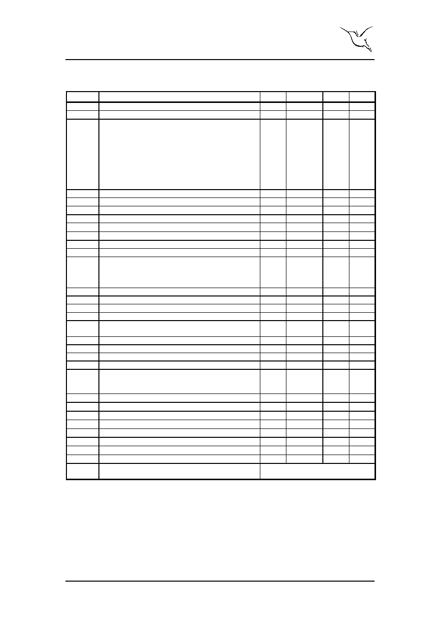
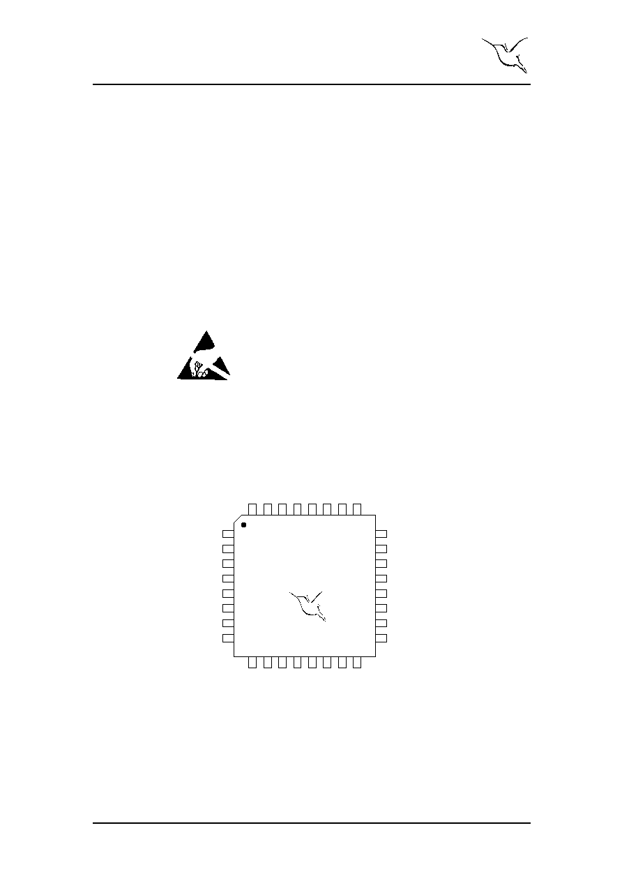
3,1 $66,*10(17
1
2
3
4
5
6
7
8
9
10
11
12
13
14
15
16
24
23
22
21
20
19
18
17
32
31
30
29
28
27
26
25
VSS
LF1
LF2
IND1
IND2
VSS
VSS
VDD
VDD
CF
G_C
L
K
CF
G_D
A
T
A
CS
XC
1
VDD
VDD
CL
K_O
U
T
VSS
VSS
FILT1
FILT2
TXEN
DATA
C_SENSE
VSS
VS
S
VD
D
VS
S
ANT
2
ANT
1
VS
S
STB
Y
PW
R
_
DW
N
Q5)
32 pin TQFP
Figure 2. nRF903 pin assignment.