 | –≠–ª–µ–∫—Ç—Ä–æ–Ω–Ω—ã–π –∫–æ–º–ø–æ–Ω–µ–Ω—Ç: nRF904 | –°–∫–∞—á–∞—Ç—å:  PDF PDF  ZIP ZIP |
PRODUCT SPECIFICATION
Main office: Nordic VLSI ASA - Vestre Rosten 81, N-7075 Tiller, Norway - Phone +4772898900 - Fax +4772898989
Revision: 2.1
Page 1 of 16
√
October 2001
Single chip 915 MHz Transmitter
)($785(6
$33/,&$7,216
∑
True single chip FSK transmitter in a
small 8-pin package
∑
Automatic Meter Reading
∑
Keyless entry
∑
Adjustable output power up to +1dBm
∑
Wireless data communication
∑
FSK data rate up to 50kbits/s
∑
Alarm and security systems
∑
Controllable modulation deviation
∑
Home Automation
∑
Very few external components
∑
Remote control
∑
Improved frequency stability compared to
SAW solutions
∑
Surveillance
∑
Automotive
∑
Wide power supply range: 2.4 to 3.6 V
∑
Telemetry
∑
Low supply current, typical 9mA
@ -10dBm output power
∑
Toys
∑
Power Down and Clock modes makes
power saving easy
∑
Reference Clock output pin for
microcontroller
*(1(5$/ '(6&5,37,21
nRF904 is a single-chip transmitter for the 902-928 MHz band. It is compliant with
the US Federal Communications Commission (FCC) standard CFR47 chapter 15. The
transmitter consists of a fully integrated frequency synthesiser, a power amplifier, a
crystal oscillator and a modulator. Due to the use of the crystal-oscillator stabilised
frequency synthesiser, frequency drift is much lower than in comparable SAW-
resonator based solutions. Output power and frequency deviation is easily
programmable by use of external resistors. Current consumption is very low, only 9
mA at an output power of ≠10dBm. Built-in Clock and Power Down modes makes
power saving easily realisable.
48,&. 5()(5(1&( '$7$
3DUDPHWHU
9DOXH
8QLW
Supply voltage
2.4 ≠ 3.6
V
Maximum output power @ 400
, 3 V
1
dBm
Maximum FSK data rate
50
kbit/s
Supply current FSK transmitter @ -10dBm output power
9
mA
Supply current in Clock mode
200
µ
A
Supply current in Power Down mode
<10
n
Table 1. nRF904 quick reference data.
7\SH 1XPEHU
'HVFULSWLRQ
9HUVLRQ
nRF904 - IC
8 pin SOIC
nRF904 - EVKIT
Evaluation kit with nRF904 IC on board
Table 2. nRF904 ordering information.
Q5)
PRODUCT SPECIFICATION
Q5) 6LQJOH FKLS 0+] 7UDQVPLWWHU
Nordic VLSI ASA - Vestre Rosten 81, N-7075 Tiller, Norway - Phone +4772898900 - Fax +4772898989
Revision: 2.1
Qhtr√!√s√ %
October 2001
%/2&. ',$*5$0
R E X T
C r y s t a l
O s c i l l a t o r
X T A L
D I N
A N T 1
F r e q u e n c y s y n t h e s i z e r
P o w e r
A m p l i f i e r
P h a s e
D e t e c t o r
V C O
L o o p
F i l t e r
P r e s c a l e r
1 / 2 5 6
A N T 2
1 / 2
C l o c k
D i v i d e r
X O 8
1 /4
Figure 1. nRF904 block diagram.
3,1 )81&7,216
3LQ
1DPH
3LQ IXQFWLRQ
'HVFULSWLRQ
1
XTAL
Input
Crystal pin / Power Up
2
REXT
Input
Power adjust / Clock Mode / ASK modulation digital input
3
XO8
Output
Reference Clock Output (Crystal Frequency / 8)
4
VDD
Power
Power Supply (+ 3 V DC)
5
DIN
Input
Digital Data Input
6
ANT2
Output
Antenna terminal
7
ANT1
Output
Antenna terminal
8
VSS
Power
Ground (0V)
Table 3. nRF904 pin functions.
3,1 $66,*10(17
DIN
VSS
7
6
5
8
ANT2
ANT1
XTAL
REXT
XO8
VDD
1
2
3
4
nRF 904
Figure 2. nRF904 pin assignment.
PRODUCT SPECIFICATION
Q5) 6LQJOH FKLS 0+] 7UDQVPLWWHU
Nordic VLSI ASA - Vestre Rosten 81, N-7075 Tiller, Norway - Phone +4772898900 - Fax +4772898989
Revision: 2.1
Qhtr√"√s√ %
October 2001
(/(&75,&$/ 63(&,),&$7,216
Conditions: VDD = +3V, VSS = 0V, T
A
= - 40∫C to + 85∫C
6\PERO 3DUDPHWHU FRQGLWLRQ�
1RWHV
0LQ
7\S
0D[
8QLWV
2SHUDWLQJ FRQGLWLRQV
f
TX
Transmit frequency
1)
902
928
MHz
f
XTAL
Crystal frequency
1)
14.094
14.500
MHz
V
DD
Supply voltage
2.4
3.6
V
Tamb
Operating temperature range
- 40
+ 85
∞
C
P
RF
Maximum Output Power
3)
1
dBm
I
DD
Supply current CLOCK Mode
2)
175
300
µ
A
I
DD
Supply current POWER DOWN Mode
10
100
nA
)6. PRGXODWLRQ
f
Frequency deviation (peak)
6)
10
20
40
kHz
R
FSK
FSK data rate
0
50
kbit/s
I
DD
Supply current @ 1dBm output power
3)
18
27
mA
I
DD
Supply current @ -10dBm output power
3)
9
17
mA
$6. PRGXODWLRQ
R
ASK
ASK data rate
0
10
kbit/s
P
RF1
Transmitted power at data = `1'
1
dBm
P
RF0
Transmitted power at data = `0'
-50
dBm
I
DD
Supply current @ 1dBm output power
3)
18
27
mA
I
DD
Supply current @ -50dBm output power
3)
175
300
uA
',1 LQSXW SLQ
V
IH
HIGH level input voltage
4)
V
DD
- 0.5
V
DD
V
V
IL
LOW level input voltage
4)
Vss
0.3
V
;2 RXWSXW SLQ
V
OH
HIGH level output voltage
5)
V
DD
V
DD
V
V
OL
LOW level output voltage
5)
V
DD
-1.0
V
NOTES:
1)
The crystal frequency may be altered to produce any desired frequency within the 902MHz to 928MHz band.
2)
Measured with no load on XO8 output pin.
3)
Antenna load impedance = 400
.
4)
The levels stated are supplied to a external series resistor in front of the DIN input pin
5)
Output is an open collector.
6)
Controllable with crystal parameters and external data filter.
Table 4. nRF904 electrical specifications.
PRODUCT SPECIFICATION
Q5) 6LQJOH FKLS 0+] 7UDQVPLWWHU
Nordic VLSI ASA - Vestre Rosten 81, N-7075 Tiller, Norway - Phone +4772898900 - Fax +4772898989
Revision: 2.1
Qhtr√#√s√ %
October 2001
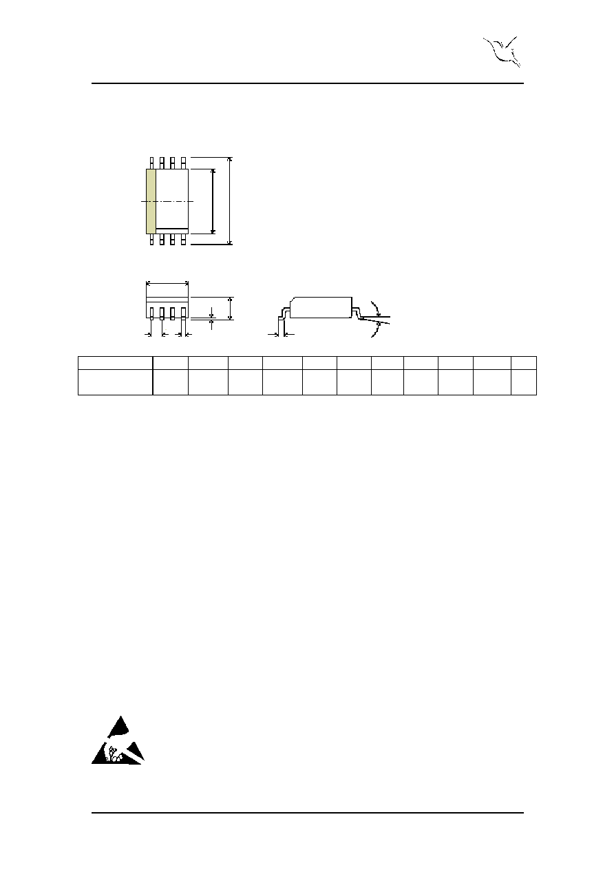
3$&.$*( 287/,1(
nRF904, uses the SOIC 8 package. Dimensions are in mm.
3DFNDJH 7\SH
'
(
+
$
$
H
E
/
&RSO
D
SOIC 8
0LQ
0D[
4.80
4.98
3.81
3.99
5.84
6.20
1.55
1.73
0.127
0.250
1.27
0.35
0.49
0.41
0.89
0.25
0
∞
8
∞
Figure 3. nRF904 package outline.
$EVROXWH 0D[LPXP 5DWLQJV
6XSSO\ YROWDJHV
VDD............................... - 0.3V to + 6V
VSS ...................................................0V
,QSXW YROWDJH
V
I
....................... - 0.3V to VDD + 0.3V
2XWSXW YROWDJH
V
O
...................... - 0.3V to VDD + 0.3V
7RWDO 3RZHU 'LVVLSDWLRQ
P
D
(T
A
=85
∞
C)............................220mW
7HPSHUDWXUHV
Operating Temperature.... - 40
∞
C to + 85
∞
C
Storage Temperature...... - 40
∞
C to + 125
∞
C
1RWH 6WUHVV H[FHHGLQJ RQH RU PRUH RI WKH OLPLWLQJ YDOXHV PD\ FDXVH SHUPDQHQW
GDPDJH WR WKH GHYLFH
$77(17,21
Electrostatic Sensitive Device
Observe Precaution for handling.
A
1
A
L
E H
D
1 2 3 4
8 7 6 5
e b
PRODUCT SPECIFICATION
Q5) 6LQJOH FKLS 0+] 7UDQVPLWWHU
Nordic VLSI ASA - Vestre Rosten 81, N-7075 Tiller, Norway - Phone +4772898900 - Fax +4772898989
Revision: 2.1
Qhtr√$√s√ %
October 2001
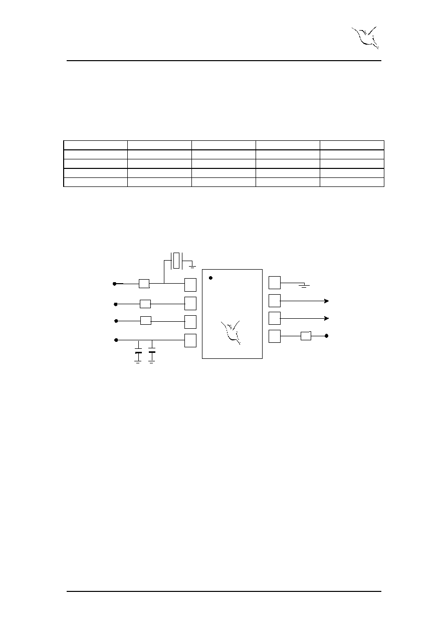
02'(6 2) 23(5$7,21
2YHUYLHZ RI 2SHUDWLRQDO 0RGHV
Table 5 provides an overview of the different modes that the nRF904 may be set to.
V
R1
to V
R4
are the control nodes for resistors 1 to 4 (R1 to R4 see Figure 4) and
represent the voltage state needed to set a particular mode.
Mode
V
R1
V
R2
V
R3
V
R4
Power Down
GND
-
-
-
Clock
VDD
GND
VDD
-
ASK
VDD
ASK DATA
VDD or GND
VDD
FSK
VDD
VDD
VDD or GND
FSK DATA
Table 5 Overview of Operational Modes for nRF904.
X1
14.2992MHz
REXT
XTAL
XO8
VDD
1
2
3
4
VDD
C
1
C
2
R2
R1
DIN
8
ANT1
ANT2
V
R1
nRF904
7
6
5
R4
R3
V
R2
V
R3
V
R4
Antenna
GND
Figure 4. nRF904 with External Components.
)6. 0RGH
FSK modulation is realised by feeding the modulating data to the digital DIN input
pin (see Figure 4). This is the normal operating mode for nRF904.
In applications where high data rate and low spectrum bandwidth is required; a low
pass filter should replace R4 as in Figure 5 to shape the input FSK bit stream. Figure 5
shows both a 1
st
order (a), and a 2
nd
order (b) low pass filter.