1/7
KGF1283
° electronic components
This version: Jul. 1998
Previous version: Jan. 1998
°
electronic components
KGF1283
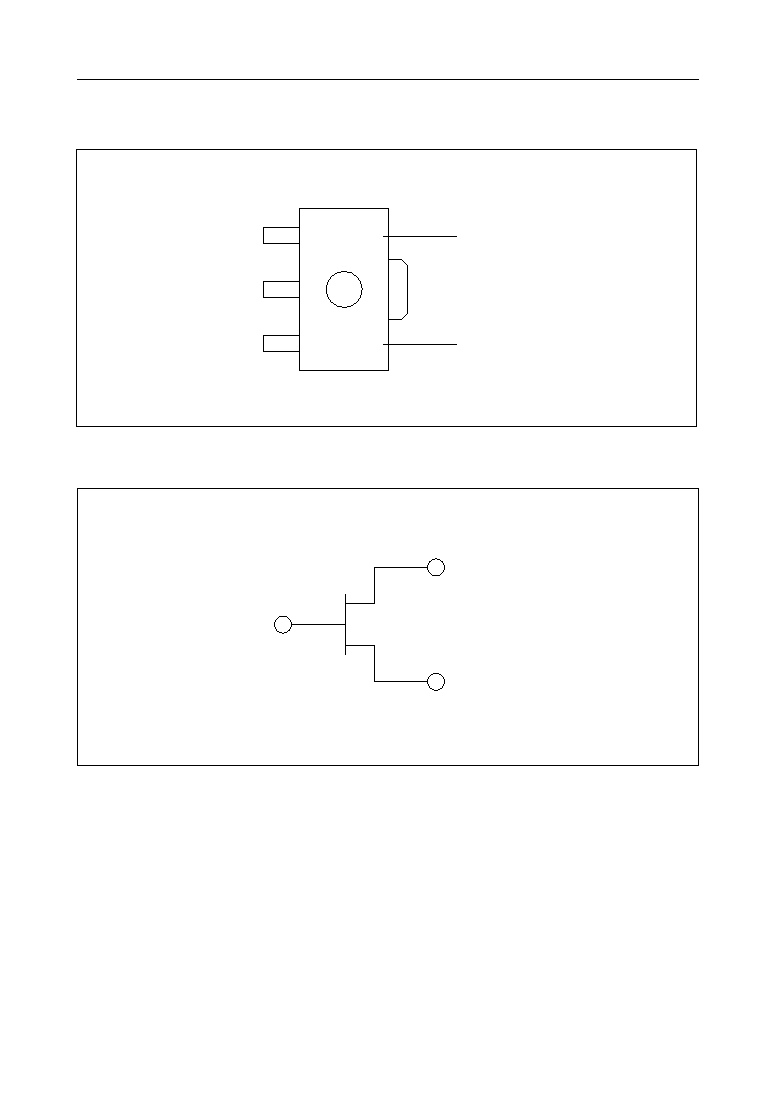
Power FET (Plastic Package Type)
GENERAL DESCRIPTION
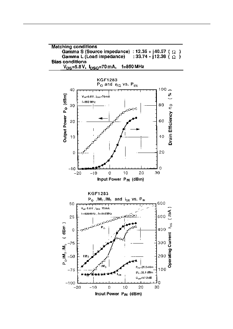
The KGF1283, housed in a SOT-89 type plastic-mold package, is a discrete UHF-band power FET
that features high efficiency, high output power, and high gain. The KGF1283 specifications are
guaranteed to a fixed matching circuit for 5.8 V and 850 MHz; external impedance-matching
circuits are also required. Because of its high efficiency, high output power (more than 26.5 dBm),
high gain, and plastic package, the KGF1283 is ideal as a transmitter-driver amplifier for personal
handy phones.
FEATURES
∑ High output power: 26.5 dBm (min.)
∑ High efficiency: 60% (typ.)
∑ High linear gain: 17 dB (typ.)
∑ Package: 3PMMP (SOT-89 type)
PACKAGE DIMENSIONS
E2Q0026-38-72
1.5
±
0.1
0.39
±
0.05
(Unit: mm)
4.5
±
0.1
4
±
0.2
2.5
±
0.1
1
±
0.2
+0.08
≠0.05
0.4
+0.08
≠0.05
0.4
+0.08
≠0.05
0.48
1.5
±
0.1 1.5
±
0.1
3
±
0.1
Package material
Pin treatment
Solder plate thickness
Lead frame material
Epoxy resin
Solder plating
5 mm or more
Cu
1.6
+0.15
≠0.10

3/7
KGF1283
° electronic components
ABSOLUTE MAXIMUM RATINGS
ELECTRICAL CHARACTERISTICS
*1 Condition: f
= 850 MHz, V
DS
= 5.8 V, I
DSQ
= 70 mA
Item
V
DS
Symbol
Condition
Max.
Unit
Drain-source voltage
Gate-source voltage
Total power dissipation
Channel temperature
V
GS
P
tot
T
ch
Ta = 25∞C
--
10
0.4
2.5
150
V
V
W
∞C
Storage temperature
T
stg
--
125
∞C
Min.
--
≠6.0
--
--
≠45
Ta = Tc = 25∞C
Ta = 25∞C
Drain current
I
DS
Ta = 25∞C
0.8
A
--
Item
P
O
Symbol
Condition
Max.
Unit
Output power
--
dBm
--
Min.
26.5
50
(*1), P
IN
= 15 dBm
Typ.
27.5
60
Drain efficiency
h
D
(*1), P
IN
= 15 dBm
%
Linear gain
G
LIN
dB
(Ta = 25∞C)
--
--
17.0
(*1), P
IN
= ≠5 dBm
Thermal resistance
R
th
∞C/W
--
--
35
Channel to case
V
GS(off)
Gate-source cut-off voltage
≠2.0
V
≠3.0
V
DS
= 3 V, I
DS
= 1.4 mA
--
I
DSS
Drain current
--
mA
450
V
DS
= 1.5 V, V
GS
= 0 V
--
I
DS(off)
Drain-source leakage current
500
mA
--
V
DS
= 10 V, V
GS
= ≠6 V
--
I
GDO
Gate-drain leakage current
150
mA
--
V
GD
= ≠16 V
--
I
GSS
Gate-source leakage current
50
mA
--
V
GS
= ≠6 V
--