1/29
° Semiconductor
MSM80C85AHRS/GS/JS
GENRAL DESCRIPTION
The MSM80C85AH is a complete 8-bit parallel; central processor implemented in silicon gate
C-MOS technology and compatible with MSM80C85A.
It is designed with higher processing speed (max.5 MHz) and lower power consumption
compared with MSM80C85A and power down mode is provided, thereby offering a high level
of system integration.
The MSM80C85AH uses a multiplexed address/data bus. The address is split between the 8-
bit address bus and the 8-bit data bus. The on-chip address latch : of a MSM81C55-5 memory
product allows a direct interface with the MSM80C85AH.
FEATURES
∑ Power down mode (HALT-HOLD)
∑ Low Power Dissipation: 50mW(Typ)
∑ Single + 3 to + 6 V Power Supply
∑ ≠40 to + 85
∞
C, Operating Temperature
∑ Compatible with MSM80C85A
∑ 0.8 ms instruction Cycle (V
CC
= 5V)
∑ On-Chip Clock Generator (with External Crystal)
∑ On-Chip System Controller; Advanced Cycle Status Information Available for Large System
Control
∑ Bug operation in MSM80C85AH is fixed
∑ Four Vectored interrupt (One is non-maskable) Plus the 8080A-compatible interrupt.
∑ Serial, In/Serial Out Port
∑ Decimal, Binary and Double Precision Arithmetic
∑ Addressing Capability to 64K Bytes of Memory
∑ TTL Compatible
∑ 40-pin Plastic DIP(DIP40-P-600-2.54): (Product name: MSM80C85AHRS)
∑ 44-pin Plastic QFJ(QFJ44-P-S650-1.27): (Product name: MSM80C85AHJS)
∑ 44-pin Plastic QFP(QFP44-P-910-0.80-2K): (Product name: MSM80C85AHGS-2K)
° Semiconductor
MSM80C85AHRS/GS/JS
8-Bit CMOS MICROPROCESSOR
E2O0009-27-X2
This version: Jan. 1998
Previous version: Aug. 1996

4/29
° Semiconductor
MSM80C85AHRS/GS/JS
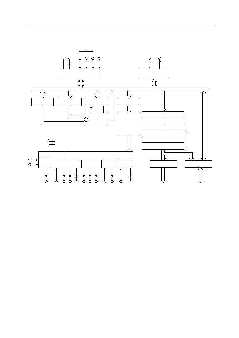
MSM80C85AH FUNCTIONAL PIN DEFINITION
The following describes the function of each pin:
A
0
- A
7
(Input/Output)
3-state
A
8
- A
15
(Output, 3-state)
Multiplexed Address/Data Bus: Lower 8-bits of the memory address (or I/O address) appear on
the bus during the first clock cycle (T state) of a machine cycle. It then becomes the data bus during
the second and third clock cycles.
Address Bus: The most significant 8-bits of the memory address or the 8-bits of the I/O address,
3-stated during Hold and Halt modes and during RESET.
Symbol
Function
ALE
(Output)
Address Latch Enable: It occurs during the first clock state of a machine cycle and enables address to
get latched into the on-chip latch peripherals. The falling edge of ALE is set to guarantee setup and
hold times for the address information. The falling edge ALE can also be used to strobe the status
information ALE is never 3-state.
S
0
, S
1
, IO/M
(Output)
Machine cycle status:
IO/M S
1
S
0
States
S
1
can be used as an advanced R/W status. IO/M, S
0
and S
1
become valid at the beginning of
a machine cycle and remain stable throughout the cycle. The falling edge of ALE may be used to latch
the state of these lines.
RD
(Output, 3-state)
READ control: A low level on RD indicates the selected memory or I/O device is to be read that
the Data Bus is available for the data transfer, 3-stated during Hold and Halt modes and during RESET.
WR
(Output, 3-state)
WRITE control: A low level on WR indicates the data on the Data Bus is to be written into the selected
memory or I/O location. Data is set up at the trailing edge of WR, 3-stated during Hold and Halt
modes and during RESET.
READY
(Input)
If READY is high during a read or write cycle, it indicates that the memory or peripheral is ready to
send or receive data. If READY is low, the cpu will wait an integral number of clock cycles for READY
to go high before completing the read or write cycle READY must conform to specified setup and
hold times.
HOLD
(Input)
HLDA
(Output)
HOLD ACKNOWLEDGE: Indicates that the cpu has received the HOLD request and that it will
relinquish the bus in the next clock cycle. HLDA goes low after the Hold request is removed.
The cpu takes the bus one half clock cycle after HLDA goes low.
HOLD indicates that another master is requesting the use of the address and data buses.
The cpu, upon receiving the hold request, will relinquish the use of the bus as soon as the completion
of the current bus transfer. Internal processing can continue. The processor can regain the bus only
after the HOLD is removed. When the HOLD is acknowledged, the Address, Data, RD, WR, and IO/M
lines are 3-stated. And status of power down is controlled by HOLD.
INTR
(Output)
INTERRUPT REQUEST: Is used as a general purpose interrupt. It is sampled on during the next to
the last clock cycle of an instruction and during Hold and Halt states. If it is active, the Program
Counter (PC) will be inhibited from incrementing and an INTA will be issued. During this cycle
a RESTART or CALL instruction can be inserted to jump to the interrupt service routine.
The INTR is enabled and disabled by software. It is disabled by Reset and immediately after
an interrupt is accepted. Power down mode is reset by INTR.
INTA
(Output)
INTERRUPT ACKNOWLEDGE: Is used instead of (and has the same timing as) RD during
the instruction cycle after an INTR is accepted.
RST 5.5
RST 6.5
RST 7.5
(Input)
RESTART INTERRUPTS: These three inputs have the same timing as INTR except they cause
an internal RESTART to be automatically inserted.
The priority of these interrupts is ordered as shown in Table 1. These interrupts have a higher priority
than INTR. In addition, they may be individually masked out using the SIM instruction.
Power down mode is reset by these interrupts.
TRAP
(Input)
Trap interrupt is a nonmaskable RESTART interrupt. It is recognized at the same timing as INTR or
RST 5.5 - 7.5. It is unaffected by any mask or Interrupt Disable. It has the highest priority of any
interrupt. (See Table 1.) Power down mode is reset by input of TRAP.
0
0
1
1
0
0
1
0
1
1
1
0
1
0
1
Memory write
Memory read
I/O write
I/O read
Opcode fetch
IO/M S
1
S
0
States
1
.
.
.
1
0
•
•
1
0
•
•
Interrupt Acknowledge
Halt = 3-state
Hold (high impedance)
Reset • = unspecified

5/29
° Semiconductor
MSM80C85AHRS/GS/JS
Name
Address Branched To (1)
When Interrupt Occurs
Type Trigger
RST 7.5
3CH
34H
Rising edge (latched).
High level unitl sampled.
RST 6.5
RST 5.5
2CH
(2)
High level until sampled.
High level until sampled.
INTR
TRAP
Priority
2
3
4
5
1
24H
Rising edge and high level unit sampled.
Table 1 Interrupt Priority, Restart Address, and Sensitivity
Notes: (1) The processor pushes the PC on the stack before branching to the indicated
address.
(2) The address branched to depends on the instruction provided to the cpu
when the interrupt is acknowledged.
RESET IN
(Input)
Sets the Program Counter to zero and resets the Interrupt Enable and HLDA flip-flops and release
power down mode. The data and address buses and the control lines are 3-stated during RESET and
because of the asynchronous nature of RESET IN, the processor's internal registers and flags may be
altered by RESET with unpredictable results. RESET IN is a Schmitt-triggered input, allowing
connection to an R-C network for power-on RESET delay. The cpu is held in the reset condition as
long as RESET IN is applied.
Symbol
Function
RESET OUT
(Output)
Indicated cpu is being reset. Can be used as a system reset. The signal is synchronized to
the processor clock and lasts an integral number of clock periods.
X
1
, X
2
(Input)
X
1
and X
2
are connected to a crystal to drive the internal clock generator. X
1
can also be an external
clock input from a logic gate. The input frequency is divided by 2 to give the processor's internal
operating frequency.
SID
(Input)
Serial input data line. The data on this line is loaded into accumulator bit 7 whenever a RIM instruction
is executed.
SOD
(Output)
Serial output data line. The output SOD is set or reset as specified by the SIM instruction.
V
CC
+ 5 Volt supply
GND
Ground Reference.
CLK
(Output)
Clock Output for use as a system clock. The period of CLK is twice the X
1
, X
2
input period.