
1/23
° Semiconductor
MSM82C54-2RS/GS/JS
GENERAL DESCRIPTION
The MSM82C54-2RS/GS/JS is a programmable universal timer designed for use in
microcomputer systems. Based on silicon gate CMOS technology, it requires a standby current
of only 10 mA (max.) when the chip is in the non-selected state. And during timer operation, the
power consumption is still very low with only 10mA (max.) of current required.
It consists of three independent counters, and can count up to a maximum of 10 MHz. The timer
features six different counter modes, and binary count/BCD count functions. Count values can
be set in byte or word units, and all functions are freely programmable.
FEATURES
∑ Maximum operating frequency of 10 MHz (V
CC
=5 V)
∑ High speed and low power consumption achieved by silicon gate CMOS technology
∑ Completely static operation
∑ Three independent 16-bit down-counters
∑ Status Read Back Command
∑ Six counter modes available for each counter
∑ Binary and decimal counting possible
∑ 24-pin Plastic DIP (DIP24-P-600-2.54): (Product name: MSM82C54-2RS)
∑ 28-pin Plastic QFJ (QFJ28-P-S450-1.27): (Product name: MSM82C54-2JS)
∑ 32-pin Plastic SSOP (SSOP32-P-430-1.00-K): (Product name: MSM82C54-2GS-K)
° Semiconductor
MSM82C54-2RS/GS/JS
CMOS PROGRAMMABLE INTERVAL TIMER
E2O0019-27-X2
This version: Jan. 1998
Previous version: Aug. 1996
5/23
° Semiconductor
MSM82C54-2RS/GS/JS
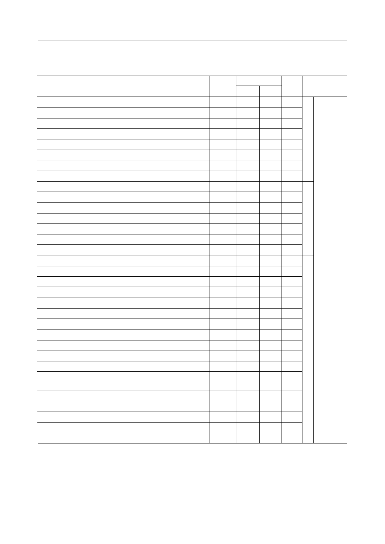
AC CHARACTERISTICS
Min.
Max.
Address Set-up Times to Falling Edge of RD
t
AR
30
--
ns
Chip Select Input Set-up Time to Falling Edge of RD
t
SR
0
--
ns
Parameter
Unit
Symbol
Conditions
Address Hold Time from Rising Edge of RD
t
RA
0
--
ns
RD Pulse Width
t
RR
95
--
ns
Data Access Time after Address Determination
t
AD
--
184
ns
Delay Time from Rising Edge of RD to Data Floting State
t
DF
5
65
ns
RD Recovery Time
t
RV
165
--
ns
Address Set-up Time to Falling Edge of WR
t
AW
0
--
ns
Chip Select Input Set-up Time to Falling Edge of WR
t
SW
0
--
ns
Address Hold Time from Rising Edge of WR
t
WA
0
--
ns
WR Pulse Width
t
WW
95
--
ns
Data Determination Set-up Time to Rising Edge of WR
t
DW
85
--
ns
Data Hold Time after Rising Edge of WR
t
WD
0
--
ns
WR Recovery Time
t
RV
165
--
ns
CLK Cycle Time
t
CLK
100
D.C.
ns
CLK "H" Level Width
t
PWH
30
--
ns
CLK "L" Level Width
t
PWL
50
--
ns
CLK Rise Time
t
r
--
25
ns
CLK Fall Time
t
f
--
25
ns
GATE "H" Level Width
t
GW
50
--
ns
GATE "L" Level Width
t
GL
50
--
ns
GATE Input Set-up Time before Rising Edge of CLK
t
GS
40
--
ns
GATE Input Hold Time before Rising Edge of CLK
t
GH
50
--
ns
Output Delay Time after Falling Edge of CLK
t
OD
--
100
ns
Output Delay Time after Falling Edge of GATE
t
ODG
--
100
ns
CLK Rise Delay Time after Rising Edge of WR for Count Value
Loading
t
WC
0
55
ns
t
WG
≠5
40
ns
GATE sampling delay time after rising edge of WR for count
loading
t
WO
--
240
ns
Output Delay Time after Falling Edge of WR for Mode Set
t
CL
≠40
40
ns
CLK Fall Set-up Time to Falling Edge of WR for Counter Latch
Command
C
L
= 150 pF
(V
CC
= 4.5 V to 5.5 V, Ta = ≠40∞C to +85∞C)
82C54-2
Data Access Time from Falling Edge of RD
t
RD
--
94
Read Timing
Write Timing
Clock Gate Timing
ns
Note:
Timing measured at V
L
= 0.8 V and V
H
= 2.2 V for both inputs and outputs.


