
©
Semiconductor Components Industries, LLC, 2003
July, 2003 - Rev. 0
1
Publication Order Number:
1PMT5920B/D
1PMT5920B Series
3.2 Watt Plastic
Surface Mount
POWERMITE
Æ
Package
This complete new line of 3.2 Watt Zener Diodes are offered in
highly efficient micro miniature, space saving surface mount with its
unique heat sink design. The POWERMITE package has the same
thermal performance as the SMA while being 50% smaller in
footprint area and delivering one of the lowest height profiles (1.1
mm) in the industry. Because of its small size, it is ideal for use in
cellular phones, portable devices, business machines and many other
industrial/consumer applications.
Specification Features:
∑
Zener Breakdown Voltage: 6.2 - 47 Volts
∑
DC Power Dissipation: 3.2 Watts with Tab 1 (Cathode) @ 75
∞
C
∑
Low Leakage < 5
mA
∑
ESD Rating of Class 3 (> 16 kV) per Human Body Model
∑
Low Profile - Maximum Height of 1.1 mm
∑
Integral Heat Sink/Locking Tabs
∑
Full Metallic Bottom Eliminates Flux Entrapment
∑
Small Footprint - Footprint Area of 8.45 mm
2
∑
Supplied in 12 mm Tape and Reel
T1 = 3,000 Units per Reel
T3 = 12,000 Units per Reel
∑
POWERMITE is JEDEC Registered as DO-216AA
∑
Cathode Indicated by Polarity Band
Mechanical Characteristics:
CASE:
Void-free, transfer-molded, thermosetting plastic
FINISH:
All external surfaces are corrosion resistant and leads are
readily solderable
MOUNTING POSITION:
Any
MAXIMUM CASE TEMPERATURE FOR SOLDERING PURPOSES:
260
∞
C for 10 Seconds
PLASTIC SURFACE MOUNT
3.2 WATT ZENER DIODES
6.2 - 47 VOLTS
Device
Package
Shipping
ORDERING INFORMATION
1PMT59xxBT1 POWERMITE 3,000/Tape & Reel
1
2
1: CATHODE
2: ANODE
LEAD ORIENTATION IN TAPE:
Cathode (Short) Lead to Sprocket Holes
xxB
= Specific Device Code
xx
= 20 - 41
=
(See Table Next Page)
D
= Date Code
POWERMITE
CASE 457
PLASTIC
1
2
MARKING DIAGRAM
xxB
D
1
CATHODE
2
ANODE
1PMT59xxBT3 POWERMITE 12,000/Tape & Reel
http://onsemi.com

Zener Voltage Regulator
I
F
V
I
I
R
I
ZT
V
R
V
Z
V
F
1PMT5920B Series
http://onsemi.com
2
MAXIMUM RATINGS
Rating
Symbol
Value
Unit
DC Power Dissipation @ T
A
= 25
∞
C (Note 1)
Derate above 25
∞
C
Thermal Resistance from Junction to Ambient
∞
P
D
∞
R
q
JA
500
4.0
248
∞
mW
mW/
∞
C
∞
C/W
Thermal Resistance from Junction to Lead (Anode)
R
q
Janode
35
∞
C/W
Maximum DC Power Dissipation (Note 2)
Thermal Resistance from Junction to Tab (Cathode)
∞
P
D
∞
R
q
Jcathode
3.2
23
W
∞
C/W
Operating and Storage Temperature Range
T
J
, T
stg
-55 to +150
∞
C
1. Mounted with recommended minimum pad size, PC board FR-4.
2. At Tab (Cathode) temperature, T
tab
= 75
∞
C
ELECTRICAL CHARACTERISTICS
(T
L
= 25
∞
C unless
otherwise noted, V
F
= 1.5 V Max. @ I
F
= 200 mAdc for all types)
Symbol
Parameter
V
Z
Reverse Zener Voltage @ I
ZT
I
ZT
Reverse Current
Z
ZT
Maximum Zener Impedance @ I
ZT
I
ZK
Reverse Current
Z
ZK
Maximum Zener Impedance @ I
ZK
I
R
Reverse Leakage Current @ V
R
V
R
Reverse Voltage
I
F
Forward Current
V
F
Forward Voltage @ I
F
ELECTRICAL CHARACTERISTICS
(T
L
= 30
∞
C unless otherwise noted, V
F
= 1.25 Volts @ 200 mA)
Zener Voltage (Note 3)
Z
ZT
@ I
ZT
Z
ZK
@ I
ZK
Device
V
Z
@ I
ZT
(Volts)
I
ZT
I
R
@ V
R
V
R
Z
ZT
@ I
ZT
(Note 4)
Z
ZK
@ I
ZK
(Note 4)
I
ZK
Device
Device
Marking
Min
Nom
Max
(mA)
(
m
A)
(V)
(
W
)
(
W
)
(mA)
1PMT5920BT1, T3
20B
5.89
6.2
6.51
60.5
5.0
4.0
2.0
200
1.0
1PMT5921BT1, T3
21B
6.46
6.8
7.14
55.1
5.0
5.2
2.5
200
1.0
1PMT5922BT1, T3
22B
7.12
7.5
7.88
50
5.0
6.0
3.0
400
0.5
1PMT5923BT1, T3
23B
7.79
8.2
8.61
45.7
5.0
6.5
3.5
400
0.5
1PMT5924BT1, T3
24B
8.64
9.1
9.56
41.2
5.0
7.0
4.0
500
0.5
1PMT5925BT1, T3
25B
9.5
10
10.5
37.5
5.0
8.0
4.5
500
0.25
1PMT5927BT1, T3
27B
11.4
12
12.6
31.2
1.0
9.1
6.5
550
0.25
1PMT5929BT1, T3
29B
14.25
15
15.75
25
1.0
11.4
9.0
600
0.25
1PMT5930BT1, T3
30B
15.2
16
16.8
23.4
1.0
12.2
10
600
0.25
1PMT5931BT1, T3
31B
17.1
18
18.9
20.8
1.0
13.7
12
650
0.25
1PMT5933BT1, T3
33B
20.9
22
23.1
17
1.0
16.7
17.5
650
0.25
1PMT5934BT1, T3
34B
22.8
24
25.2
15.6
1.0
18.2
19
700
0.25
1PMT5935BT1, T3
35B
25.65
27
28.35
13.9
1.0
20.6
23
700
0.25
1PMT5936BT1, T3
36B
28.5
30
31.5
12.5
1.0
22.8
28
750
0.25
1PMT5939BT1, T3
39B
37.05
39
40.95
9.6
1.0
29.7
45
900
0.25
1PMT5941BT1, T3
41B
44.65
47
49.35
8.0
1.0
35.8
67
1000
0.25
3. Zener voltage is measured with the device junction in thermal equilibrium with an ambient temperature of 25
∞
C.
4. Zener Impedance Derivation Z
ZT
and Z
ZK
are measured by dividing the AC voltage drop across the device by the AC current applied. The
specified limits are for I
Z
(ac) = 0.1 I
Z
(dc) with the ac frequency = 60 Hz.

1PMT5920B Series
http://onsemi.com
3
TYPICAL CHARACTERISTICS
7
5
3
2
Figure 1. Steady State Power Derating
Figure 2. V
Z
to 10 Volts
25
50
75
100
125
175
3.5
2.5
2
1.5
1
0
T, TEMPERATURE (
∞
C)
P
, MAXIMUM POWER DISSIP
A
TION (W)
D
0.1
5
6
9
10
V
Z
, ZENER VOLTAGE (VOLTS)
0.5
T
L
2
4
6
8
10
12
10
8
6
4
2
0
-2
-4
V
Z
, ZENER VOLTAGE (VOLTS)
V
Z
@ I
ZT
200
100
70
50
30
20
10
10
20
30
50
70
100
200
V
Z
, ZENER VOLTAGE (VOLTS)
V
Z
@ I
ZT
150
3
7
8
11
1
10
100
I
Z
, ZENER CURRENT (mA)
Figure 3. V
Z
= 12 thru 47 Volts
0
10
20
30
40
50
60
70
80
90
100
V
Z
, ZENER VOLTAGE (VOLTS)
I , ZENER CURRENT
(mA)
Z
100
50
30
20
10
1
0.5
0.3
0.2
0.1
2
5
3
Figure 4. Zener Voltage - To 12 Volts
Figure 5. Zener Voltage - 14 To 47 Volts
Figure 6. Effect of Zener Voltage
V
Z
, ZENER VOLTAGE (VOLTS)
5
7
10
20
30
50
70
100
200
100
70
50
30
20
10
Z , DYNAMIC IMPEDANCE (OHMS)
Z
I
Z(dc)
= 1mA
20
mA
i
Z(rms)
= 0.1 I
Z(dc)
10
mA
q
VZ
, TEMPERA
TURE COEFFICIENT (mV/
∞
C)
q
VZ
, TEMPERA
TURE COEFFICIENT (mV/
∞
C)
1PMT5920B Series
http://onsemi.com
4
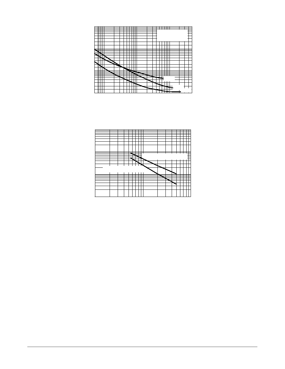
Figure 7. Effect of Zener Current
I
Z
, ZENER TEST CURRENT (mA)
1 k
500
200
100
50
20
10
5
2
1
0.5
1
2
5
10
20
50
100 200
500
Z , DYNAMIC IMPEDANCE (OHMS)
Z
T
J
= 25
∞
C
i
Z(rms)
= 0.1 I
Z(dc)
22
V
12
V
6.8 V
10,000
1000
100
10
1
10
V
Z
, REVERSE ZENER VOLTAGE (VOLTS)
C, CAP
ACIT
ANCE (pF)
MEASURED @ 50% V
R
MEASURED @ 0 V BIAS
Figure 8. Capacitance versus Reverse
Zener Voltage
100

1PMT5920B Series
http://onsemi.com
5
TYPICAL SOLDER HEATING PROFILE
For any given circuit board, there will be a group of
control settings that will give the desired heat pattern. The
operator must set temperatures for several heating zones
and a figure for belt speed. Taken together, these control
settings make up a heating "profile" for that particular
circuit board. On machines controlled by a computer, the
computer remembers these profiles from one operating
session to the next. Figure 9 shows a typical heating profile
for use when soldering a surface mount device to a printed
circuit board. This profile will vary among soldering
systems, but it is a good starting point. Factors that can
affect the profile include the type of soldering system in
use, density and types of components on the board, type of
solder used, and the type of board or substrate material
being used. This profile shows temperature versus time.
The line on the graph shows the actual temperature that
might be experienced on the surface of a test board at or
near a central solder joint. The two profiles are based on a
high density and a low density board. The Vitronics
SMD310 convection/infrared reflow soldering system was
used to generate this profile. The type of solder used was
62/36/2 Tin Lead Silver with a melting point between
177 -189
∞
C. When this type of furnace is used for solder
reflow work, the circuit boards and solder joints tend to
heat first. The components on the board are then heated by
conduction. The circuit board, because it has a large surface
area, absorbs the thermal energy more efficiently, then
distributes this energy to the components. Because of this
effect, the main body of a component may be up to 30
degrees cooler than the adjacent solder joints.
STEP 1
PREHEAT
ZONE 1
RAMP"
STEP 2
VENT
SOAK"
STEP 3
HEATING
ZONES 2 & 5
RAMP"
STEP 4
HEATING
ZONES 3 & 6
SOAK"
STEP 5
HEATING
ZONES 4 & 7
SPIKE"
STEP 6
VENT
STEP 7
COOLING
200
∞
C
150
∞
C
100
∞
C
50
∞
C
TIME (3 TO 7 MINUTES TOTAL)
T
MAX
SOLDER IS LIQUID FOR
40 TO 80 SECONDS
(DEPENDING ON
MASS OF ASSEMBLY)
205
∞
TO 219
∞
C
PEAK AT
SOLDER JOINT
DESIRED CURVE FOR LOW
MASS ASSEMBLIES
100
∞
C
150
∞
C
160
∞
C
170
∞
C
140
∞
C
Figure 9. Typical Solder Heating Profile
DESIRED CURVE FOR HIGH
MASS ASSEMBLIES

1PMT5920B Series
http://onsemi.com
6
INFORMATION FOR USING THE POWERMITE SURFACE MOUNT PACKAGE
MINIMUM RECOMMENDED FOOTPRINT FOR SURFACE MOUNTED APPLICATIONS
Surface mount board layout is a critical portion of the
total design. The footprint for the semiconductor packages
must be the correct size to insure proper solder connection
interface between the board and the package. With the
correct pad geometry, the packages will self align when
subjected to a solder reflow process.
POWERMITE
0.100
2.54
0.025
0.635
0.050
1.27
0.105
2.67
0.030
0.762
inches
mm
POWERMITE POWER DISSIPATION
The power dissipation of the Powermite is a function of
the drain pad size. This can vary from the minimum pad
size for soldering to a pad size given for maximum power
dissipation. Power dissipation for a surface mount device is
determined by T
J(max)
, the maximum rated junction
temperature of the die, R
qJA
, the thermal resistance from
the device junction to ambient, and the operating
temperature, T
A
. Using the values provided on the data
sheet for the Powermite package, P
D
can be calculated as
follows:
P
D
=
T
J(max)
- T
A
R
q
JA
The values for the equation are found in the maximum
ratings table on the data sheet. Substituting these values
into the equation for an ambient temperature T
A
of 25
∞
C,
one can calculate the power dissipation of the device which
in this case is 504 milliwatts.
P
D
= 150
∞
C - 25
∞
C = 504 milliwatts
248
∞
C/W
The 248
∞
C/W for the Powermite package assumes the
use of the recommended footprint on a glass epoxy printed
circuit board to achieve a power dissipation of 504
milliwatts. There are other alternatives to achieving higher
power dissipation from the Powermite package. Another
alternative would be to use a ceramic substrate or an
aluminum core board such as Thermal Clad
TM
. Using a
board material such as Thermal Clad, an aluminum core
board, the power dissipation can be doubled using the same
footprint.
SOLDERING PRECAUTIONS
The melting temperature of solder is higher than the rated
temperature of the device. When the entire device is heated
to a high temperature, failure to complete soldering within
a short time could result in device failure. Therefore, the
following items should always be observed in order to
minimize the thermal stress to which the devices are
subjected.
∑
Always preheat the device.
∑
The delta temperature between the preheat and
soldering should be 100
∞
C or less.*
∑
When preheating and soldering, the temperature of the
leads and the case must not exceed the maximum
temperature ratings as shown on the data sheet. When
using infrared heating with the reflow soldering
method, the difference shall be a maximum of 10
∞
C.
∑
The soldering temperature and time shall not exceed
260
∞
C for more than 10 seconds.
∑
When shifting from preheating to soldering, the
maximum temperature gradient shall be 5
∞
C or less.
∑
After soldering has been completed, the device should
be allowed to cool naturally for at least three minutes.
Gradual cooling should be used as the use of forced
cooling will increase the temperature gradient and
result in latent failure due to mechanical stress.
∑
Mechanical stress or shock should not be applied
during cooling.
* * Soldering a device without preheating can cause
excessive thermal shock and stress which can result in
damage to the device.

1PMT5920B Series
http://onsemi.com
7
OUTLINE DIMENSIONS
1PMT5920BT3 Series - Surface Mounted
DIM
MIN
MAX
MIN
MAX
INCHES
MILLIMETERS
A
1.75
2.05
0.069
0.081
B
1.75
2.18
0.069
0.086
C
0.85
1.15
0.033
0.045
D
0.40
0.69
0.016
0.027
F
0.70
1.00
0.028
0.039
H
-0.05
+0.10 -0.002 +0.004
J
0.10
0.25
0.004
0.010
K
3.60
3.90
0.142
0.154
L
0.50
0.80
0.020
0.031
R
1.20
1.50
0.047
0.059
S
NOTES:
1. DIMENSIONING AND TOLERANCING PER ANSI
Y14.5M, 1982.
2. CONTROLLING DIMENSION: MILLIMETER.
3. DIMENSION A DOES NOT INCLUDE MOLD FLASH,
PROTRUSIONS OR GATE BURRS. MOLD FLASH,
PROTRUSIONS OR GATE BURRS SHALL NOT
EXCEED 0.15 (0.006) PER SIDE.
S
B
M
0.08 (0.003)
C
S
T
-A-
-B-
S
J
K
-T-
H
L
J
C
D
S
B
M
0.08 (0.003)
C
S
T
F
TERM. 1
TERM. 2
R
0.50 REF
0.019 REF
POWERMITE
CASE 457-04
ISSUE D

1PMT5920B Series
http://onsemi.com
8
ON Semiconductor and are registered trademarks of Semiconductor Components Industries, LLC (SCILLC). SCILLC reserves the right to make
changes without further notice to any products herein. SCILLC makes no warranty, representation or guarantee regarding the suitability of its products for any
particular purpose, nor does SCILLC assume any liability arising out of the application or use of any product or circuit, and specifically disclaims any and all
liability, including without limitation special, consequential or incidental damages. "Typical" parameters which may be provided in SCILLC data sheets and/or
specifications can and do vary in different applications and actual performance may vary over time. All operating parameters, including "Typicals" must be
validated for each customer application by customer's technical experts. SCILLC does not convey any license under its patent rights nor the rights of others.
SCILLC products are not designed, intended, or authorized for use as components in systems intended for surgical implant into the body, or other applications
intended to support or sustain life, or for any other application in which the failure of the SCILLC product could create a situation where personal injury or death
may occur. Should Buyer purchase or use SCILLC products for any such unintended or unauthorized application, Buyer shall indemnify and hold SCILLC
and its officers, employees, subsidiaries, affiliates, and distributors harmless against all claims, costs, damages, and expenses, and reasonable attorney fees
arising out of, directly or indirectly, any claim of personal injury or death associated with such unintended or unauthorized use, even if such claim alleges that
SCILLC was negligent regarding the design or manufacture of the part. SCILLC is an Equal Opportunity/Affirmative Action Employer.
PUBLICATION ORDERING INFORMATION
JAPAN: ON Semiconductor, Japan Customer Focus Center
2-9-1 Kamimeguro, Meguro-ku, Tokyo, Japan 153-0051
Phone: 81-3-5773-3850
ON Semiconductor Website: http://onsemi.com
For additional information, please contact your local
Sales Representative.
1PMT5920B/D
POWERMITE is a registered trademark of and used under a license from Microsemi Corporation.
Thermal Clad is a trademark of the Bergquist Corporation.
Literature Fulfillment:
Literature Distribution Center for ON Semiconductor
P.O. Box 5163, Denver, Colorado 80217 USA
Phone: 303-675-2175 or 800-344-3860 Toll Free USA/Canada
Fax: 303-675-2176 or 800-344-3867 Toll Free USA/Canada
Email: orderlit@onsemi.com
N. American Technical Support: 800-282-9855 Toll Free USA/Canada