
©
Semiconductor Components Industries, LLC, 2004
April, 2004 - Rev. 4
1
Publication Order Number:
1SMA5913BT3/D
1SMA5913BT3 Series
1.5 Watt Plastic
Surface Mount
Zener Voltage Regulators
This complete new line of 1.5 Watt Zener Diodes offers the
following advantages.
Specification Features
∑
Standard Zener Breakdown Voltage Range - 3.3 V to 68 V
∑
ESD Rating of Class 3 (>16 kV) per Human Body Model
∑
Flat Handling Surface for Accurate Placement
∑
Package Design for Top Slide or Bottom Circuit Board Mounting
∑
Low Profile Package
∑
Ideal Replacement for MELF Packages
∑
Pb-Free Packages are Available
Mechanical Characteristics:
CASE:
Void-free, transfer-molded plastic
FINISH:
All external surfaces are corrosion resistant with readily
solderable leads
MAXIMUM CASE TEMPERATURE FOR SOLDERING PURPOSES:
260
∞
C for 10 seconds
POLARITY:
Cathode indicated by molded polarity notch or cathode
band
FLAMMABILITY RATING:
UL 94 V-0 @ 0.125 in
MAXIMUM RATINGS
Rating
Symbol
Value
Unit
DC Power Dissipation @ T
L
= 75
∞
C,
Measured Zero Lead Length (Note 1.)
Derate above 75
∞
C
Thermal Resistance -
Junction-to-Lead
P
D
R
q
JL
1.5
20
50
Watts
mW/
∞
C
∞
C/W
DC Power Dissipation @ T
A
= 25
∞
C
(Note 2.) Derate above 25
∞
C
Thermal Resistance -
Junction-to-Ambient
P
D
R
q
JA
0.5
4.0
250
Watts
mW/
∞
C
∞
C/W
Operating and Storage
Temperature Range
T
J
, T
stg
-65 to
+150
∞
C
Maximum ratings are those values beyond which device damage can occur.
Maximum ratings applied to the device are individual stress limit values (not
normal operating conditions) and are not valid simultaneously. If these limits
are exceeded, device functional operation is not implied, damage may occur
and reliability may be affected.
1. 1
square copper pad, FR-4 board
2. FR-4 Board, using ON Semiconductor minimum recommended footprint
SMA
CASE 403D
PLASTIC
8xxB
= Specific Device Code
=
(See Table Next Page)
LL
= Assembly Location
Y
= Year
WW
= Work Week
8xxB
LLYWW
MARKING DIAGRAM
CATHODE
ANODE
Device
*
Package
Shipping
ORDERING INFORMATION
1SMA59xxBT3
SMA
5000/Tape & Reel
*The "T3" suffix refers to a 13 inch reel.
http://onsemi.com
1SMA59xxBT3G
SMA
(Pb-Free)
5000/Tape & Reel
Individual devices are listed on page 2 of this data sheet.
For information on tape and reel specifications,
including part orientation and tape sizes, please
refer to our Tape and Reel Packaging Specifications
Brochure, BRD8011/D.
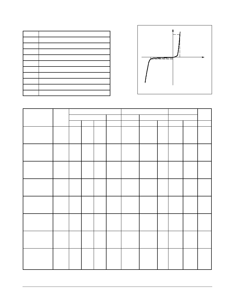
Zener Voltage Regulator
I
F
V
I
I
R
I
ZT
V
R
V
Z
V
F
1SMA5913BT3 Series
http://onsemi.com
2
ELECTRICAL CHARACTERISTICS
(T
A
= 25
∞
C unless
otherwise noted, V
F
= 1.5 V Max. @ I
F
= 200 mA for all types)
Symbol
Parameter
V
Z
Reverse Zener Voltage @ I
ZT
I
ZT
Reverse Current
Z
ZT
Maximum Zener Impedance @ I
ZT
I
ZK
Reverse Current
Z
ZK
Maximum Zener Impedance @ I
ZK
I
R
Reverse Leakage Current @ V
R
V
R
Reverse Voltage
I
F
Forward Current
V
F
Forward Voltage @ I
F
I
ZM
Maximum DC Zener Current
ELECTRICAL CHARACTERISTICS
(T
A
= 25
∞
C unless otherwise noted, V
F
= 1.5 V Max. @ I
F
= 200 mA for all types)
Zener Voltage (Note 2)
Zener Impedance
Leakage Current
Device
V
Z
(Volts)
@ I
ZT
Z
ZT
@ I
ZT
Z
ZK
@ I
ZK
I
R
@ V
R
I
ZM
Device (Note 1)
Device
Marking
Min
Nom
Max
mA
W
W
mA
m
A
Volts
mA(dc)
1SMA5913BT3
813B
3.13
3.3
3.47
113.6
10
500
1.0
50
1.0
455
1SMA5914BT3
814B
3.42
3.6
3.78
104.2
9.0
500
1.0
35.5
1.0
417
1SMA5915BT3
815B
3.70
3.9
4.10
96.1
7.5
500
1.0
12.5
1.0
385
1SMA5916BT3
816B
4.08
4.3
4.52
87.2
6.0
500
1.0
2.5
1.0
349
1SMA5917BT3
817B
4.46
4.7
4.94
79.8
5.0
500
1.0
2.5
1.5
319
1SMA5918BT3
818B
4.84
5.1
5.36
73.5
4.0
350
1.0
2.5
2.0
294
1SMA5919BT3
819B
5.32
5.6
5.88
66.9
2.0
250
1.0
2.5
3.0
268
1SMA5920BT3
820B
5.89
6.2
6.51
60.5
2.0
200
1.0
2.5
4.0
242
1SMA5921BT3
821B
6.46
6.8
7.14
55.1
2.5
200
1.0
2.5
5.2
221
1SMA5922BT3
822B
7.12
7.5
7.88
50
3.0
400
0.5
2.5
6.0
200
1SMA5923BT3
823B
7.79
8.2
8.61
45.7
3.5
400
0.5
2.5
6.5
183
1SMA5924BT3, G*
824B
8.64
9.1
9.56
41.2
4.0
500
0.5
2.5
7.0
165
1SMA5925BT3
825B
9.5
10
10.5
37.5
4.5
500
0.25
2.5
8.0
150
1SMA5926BT3
826B
10.45
11
11.55
34.1
5.5
550
0.25
0.5
8.4
136
1SMA5927BT3, G*
827B
11.4
12
12.6
31.2
6.5
550
0.25
0.5
9.1
125
1SMA5928BT3
828B
12.35
13
13.65
28.8
7.0
550
0.25
0.5
9.9
115
1SMA5929BT3, G*
829B
14.25
15
15.75
25
9.0
600
0.25
0.5
11.4
100
1SMA5930BT3
830B
15.2
16
16.8
23.4
10
600
0.25
0.5
12.2
94
1SMA5931BT3
831B
17.1
18
18.9
20.8
12
650
0.25
0.5
13.7
83
1SMA5932BT3
832B
19
20
21
18.7
14
650
0.25
0.5
15.2
75
1SMA5933BT3
833B
20.9
22
23.1
17
17.5
650
0.25
0.5
16.7
68
1SMA5934BT3
834B
22.8
24
25.2
15.6
19
700
0.25
0.5
18.2
63
1SMA5935BT3
835B
25.65
27
28.35
13.9
23
700
0.25
0.5
20.6
56
1SMA5936BT3
836B
28.5
30
31.5
12.5
26
750
0.25
0.5
22.8
50
1SMA5937BT3
837B
31.35
33
34.65
11.4
33
800
0.25
0.5
25.1
45
1SMA5938BT3
838B
34.2
36
37.8
10.4
38
850
0.25
0.5
27.4
42
1SMA5939BT3
839B
37.05
39
40.95
9.6
45
900
0.25
0.5
29.7
38
1SMA5940BT3, G*
840B
40.85
43
45.15
8.7
53
950
0.25
0.5
32.7
35
1SMA5941BT3
841B
44.65
47
49.35
8.0
67
1000
0.25
0.5
35.8
32
1SMA5942BT3
842B
48.45
51
53.55
7.3
70
1100
0.25
0.5
38.8
29
1SMA5943BT3, G*
843B
53.2
56
58.8
6.7
86
1300
0.25
0.5
42.6
27
1SMA5944BT3
844B
58.9
62
65.1
6.0
100
1500
0.25
0.5
47.1
24
1SMA5945BT3
845B
64.6
68
71.4
5.5
120
1700
0.25
0.5
51.7
22
1. Tolerance and Voltage Regulation Designation - The type number listed indicates a tolerance of
±
5%.
2. V
Z
limits are to be guaranteed at thermal equilibrium.
* The "G" suffix indicates Pb-Free package available.

1SMA5913BT3 Series
http://onsemi.com
3
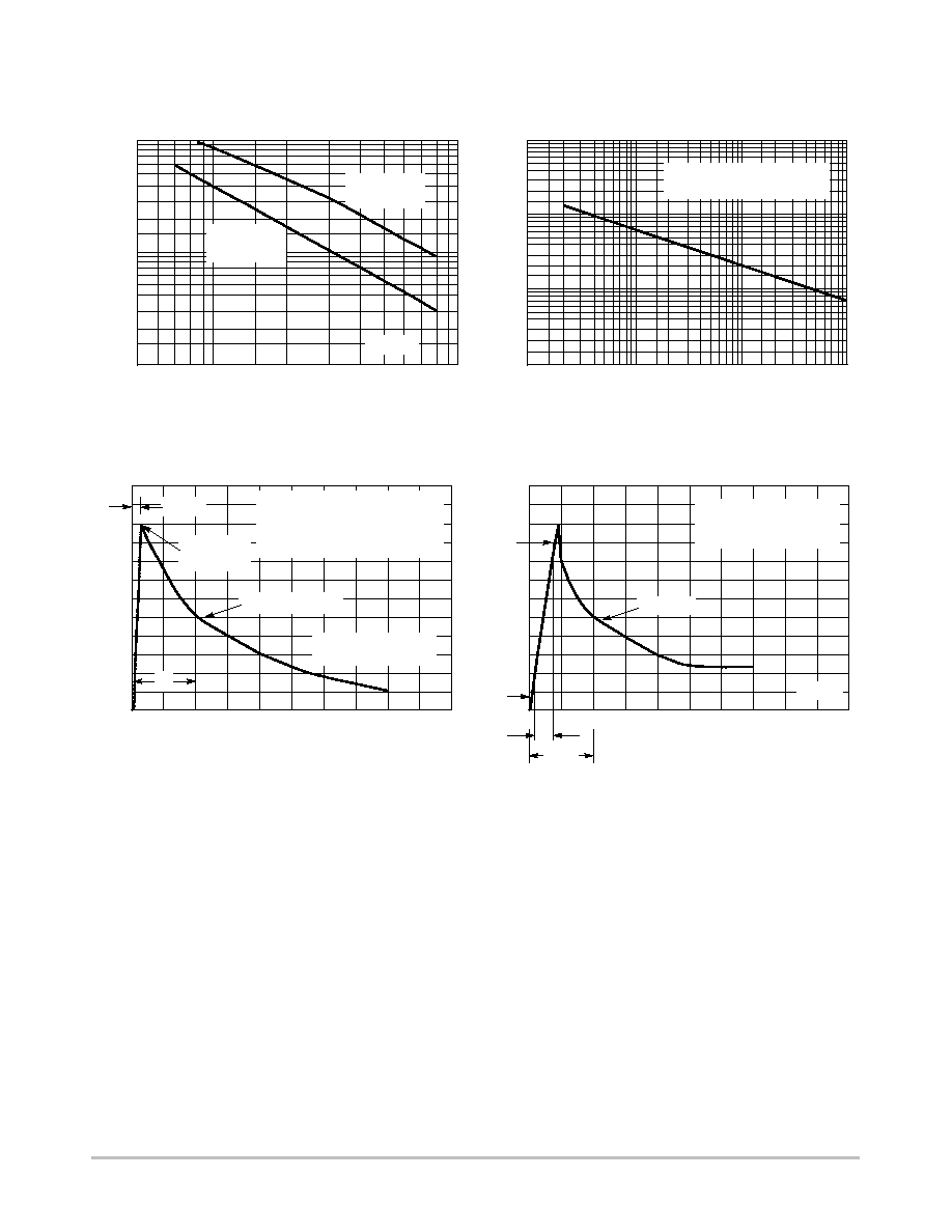
Rating and Typical Characteristic Curves (T
A
= 25
∞
C)
VZ
,
TEMPERA
TURE COEFFICIENT
(mV/
C)
∞
0
4
Figure 1. Steady State Power Derating
Figure 2. V
Z
- 3.3 thru 10 Volts
T, TEMPERATURE (
∞
C)
Figure 3. V
Z
= 12 thru 68 Volts
25
50
75
100
125
150
P
D
, MAXIMUM POWER DISSIP
A
TION (W
A
TTS)
I Z
, ZENER CURRENT
(mA)
Z Z
, DYNAMIC IMPEDANCE (OHMS)
3.2
2.4
1.6
0.8
0
0
100
2
4
6
8
10
10
1
0.1
V
Z
, ZENER VOLTAGE (VOLTS)
100
10
1
0.1
0
10
20
30
40
V
Z
, ZENER VOLTAGE (VOLTS)
100
10
10
100
V
Z
, ZENER VOLTAGE (VOLTS)
T
L
T
A
V
Z
@ I
ZT
10
100
V
Z
, ZENER VOLTAGE (VOLTS)
I
Z(dc)
= 1 mA
100
10
10 mA
20 mA
I
Z(rms)
= 0.1 I
Z(dc)
50
Figure 4. Zener Voltage - 3.3 to 12 Volts
VZ
,
TEMPERA
TURE COEFFICIENT
(mV/
C)
∞
10
8
6
4
2
0
-2
-4
2
4
6
8
10
V
Z
, ZENER VOLTAGE (VOLTS)
V
Z
@ I
ZT
12
Figure 5. Zener Voltage - 14 to 68 Volts
Figure 6. Effect of Zener Voltage
I
Z
, ZENER CURRENT (mA)
60
70
80
1SMA5913BT3 Series
http://onsemi.com
4
Rating and Typical Characteristic Curves (T
A
= 25
∞
C)
T
A
= 25
∞
C
PW (I
D
) IS DEFINED AS THE
POINT WHERE THE PEAK CURRENT
DECAYS TO 50% OF I
pp
.
10 ms
PEAK VALUE
I
ppm
HALF VALUE - I
pp
/2
10/1000 ms WAVEFORM
AS DEFINED BY R.E.A.
t
d
1000
Figure 7. Capacitance Curve
Figure 8. Typical Pulse Rating Curve
BREAKDOWN VOLTAGE (VOLTS)
Figure 9. Pulse Waveform
Figure 10. Pulse Waveform
10
100
100
10
0.01
10
0.1
1
10
1
0.1
0.01
T
P
, PULSE WIDTH (ms)
120
100
80
60
40
0
0
1
2
3
4
t, TIME (ms)
120
0
0.1
t, TIME (ms)
MEASURED @
ZERO BIAS
MEASURED @
V
Z
/2
T
J
= 25
∞
C
C, CAP
ACIT
ANCE (pF)
P pk
I ppm
, PEAK PULSE CURRENT
(%)
NONREPETITIVE, EXPONENTIAL
PULSE WAVEFORM, T
J
= 25
∞
C
20
5
100
80
60
40
20
0.04
0.06
0.08
8/20 ms WAVEFORM
AS DEFINED BY ANSI C62.1
AND IEC 801-5.
0.5 I
PEAK
0.9 I
PEAK
0.1 I
PEAK
T
T = 8 ms
20 ms
0
0.02
I ppm
, PEAK PULSE
CURRENT
(%)
, PEAK POWER (kW)
1SMA5913BT3 Series
http://onsemi.com
5
OUTLINE DIMENSIONS
SMA
CASE 403D-02
ISSUE A
S
A
D
B
K
J
C
H
DIM
MIN
MAX
MIN
MAX
MILLIMETERS
INCHES
A
0.160
0.180
4.06
4.57
B
0.090
0.115
2.29
2.92
C
0.075
0.095
1.91
2.41
D
0.050
0.064
1.27
1.63
H
0.002
0.006
0.05
0.15
J
0.006
0.016
0.15
0.41
K
0.030
0.060
0.76
1.52
S
0.190
0.220
4.83
5.59
POLARITY INDICATOR OPTIONAL
AS NEEDED
NOTES:
1. DIMENSIONING AND TOLERANCING PER ANSI
Y14.5M, 1982.
2. CONTROLLING DIMENSION: INCH.
3. 403D-01 OBSOLETE, NEW STANDARD IS
403D-02.
4.0
0.157
2.0
0.0787
2.0
0.0787
mm
inches
SCALE 8:1
*For additional information on our Pb-Free strategy and soldering
details, please download the ON Semiconductor Soldering and
Mounting Techniques Reference Manual, SOLDERRM/D.
SOLDERING FOOTPRINT*
1SMA5913BT3 Series
http://onsemi.com
6
ON Semiconductor and are registered trademarks of Semiconductor Components Industries, LLC (SCILLC). SCILLC reserves the right to make changes without further notice
to any products herein. SCILLC makes no warranty, representation or guarantee regarding the suitability of its products for any particular purpose, nor does SCILLC assume any liability
arising out of the application or use of any product or circuit, and specifically disclaims any and all liability, including without limitation special, consequential or incidental damages.
"Typical" parameters which may be provided in SCILLC data sheets and/or specifications can and do vary in different applications and actual performance may vary over time. All
operating parameters, including "Typicals" must be validated for each customer application by customer's technical experts. SCILLC does not convey any license under its patent rights
nor the rights of others. SCILLC products are not designed, intended, or authorized for use as components in systems intended for surgical implant into the body, or other applications
intended to support or sustain life, or for any other application in which the failure of the SCILLC product could create a situation where personal injury or death may occur. Should
Buyer purchase or use SCILLC products for any such unintended or unauthorized application, Buyer shall indemnify and hold SCILLC and its officers, employees, subsidiaries, affiliates,
and distributors harmless against all claims, costs, damages, and expenses, and reasonable attorney fees arising out of, directly or indirectly, any claim of personal injury or death
associated with such unintended or unauthorized use, even if such claim alleges that SCILLC was negligent regarding the design or manufacture of the part. SCILLC is an Equal
Opportunity/Affirmative Action Employer. This literature is subject to all applicable copyright laws and is not for resale in any manner.
PUBLICATION ORDERING INFORMATION
N. American Technical Support: 800-282-9855 Toll Free
USA/Canada
Japan: ON Semiconductor, Japan Customer Focus Center
2-9-1 Kamimeguro, Meguro-ku, Tokyo, Japan 153-0051
Phone: 81-3-5773-3850
1SMA5913BT3/D
LITERATURE FULFILLMENT:
Literature Distribution Center for ON Semiconductor
P.O. Box 5163, Denver, Colorado 80217 USA
Phone: 303-675-2175 or 800-344-3860 Toll Free USA/Canada
Fax: 303-675-2176 or 800-344-3867 Toll Free USA/Canada
Email: orderlit@onsemi.com
ON Semiconductor Website: http://onsemi.com
Order Literature: http://www.onsemi.com/litorder
For additional information, please contact your
local Sales Representative.