 | ÐлекÑÑоннÑй компоненÑ: 2N3773 | СкаÑаÑÑ:  PDF PDF  ZIP ZIP |
Äîêóìåíòàöèÿ è îïèñàíèÿ www.docs.chipfind.ru
1
Motorola Bipolar Power Transistor Device Data
Complementary Silicon Power
Transistors
The 2N3773 and 2N6609 are PowerBase power transistors designed for high
power audio, disk head positioners and other linear applications. These devices can
also be used in power switching circuits such as relay or solenoid drivers, dc to dc
converters or inverters.
·
High Safe Operating Area (100% Tested) 150 W @ 100 V
·
Completely Characterized for Linear Operation
·
High DC Current Gain and Low Saturation Voltage
hFE = 15 (Min) @ 8 A, 4 V
VCE(sat) = 1.4 V (Max) @ IC = 8 A, IB = 0.8 A
·
For Low Distortion Complementary Designs
ÎÎÎÎÎÎÎÎÎÎÎÎÎÎÎÎÎÎÎÎÎÎÎÎÎÎÎÎÎÎÎÎÎÎ
ÎÎÎÎÎÎÎÎÎÎÎÎÎÎÎÎÎÎÎÎÎÎÎÎÎÎÎÎÎÎÎÎÎÎ
ÎÎÎÎÎÎÎÎÎÎÎÎÎÎÎÎÎÎÎÎÎÎÎÎÎÎÎÎÎÎÎÎÎÎ
ÎÎÎÎÎÎÎÎÎÎÎÎÎÎÎÎÎÎÎÎÎÎÎÎÎÎÎÎÎÎÎÎÎÎ
*MAXIMUM RATINGS
ÎÎÎÎÎÎÎÎÎÎÎÎÎÎÎÎÎÎ
ÎÎÎÎÎÎÎÎÎÎÎÎÎÎÎÎÎÎ
ÎÎÎÎÎÎÎÎÎÎÎÎÎÎÎÎÎÎ
ÎÎÎÎÎÎÎÎÎÎÎÎÎÎÎÎÎÎ
Rating
ÎÎÎÎÎÎÎ
ÎÎÎÎÎÎÎ
ÎÎÎÎÎÎÎ
ÎÎÎÎÎÎÎ
Symbol
ÎÎÎÎÎÎÎÎ
ÎÎÎÎÎÎÎÎ
ÎÎÎÎÎÎÎÎ
ÎÎÎÎÎÎÎÎ
Value
ÎÎÎÎ
ÎÎÎÎ
ÎÎÎÎ
ÎÎÎÎ
Unit
ÎÎÎÎÎÎÎÎÎÎÎÎÎÎÎÎÎÎ
ÎÎÎÎÎÎÎÎÎÎÎÎÎÎÎÎÎÎ
ÎÎÎÎÎÎÎÎÎÎÎÎÎÎÎÎÎÎ
ÎÎÎÎÎÎÎÎÎÎÎÎÎÎÎÎÎÎ
Collector Emitter Voltage
ÎÎÎÎÎÎÎ
ÎÎÎÎÎÎÎ
ÎÎÎÎÎÎÎ
ÎÎÎÎÎÎÎ
VCEO
ÎÎÎÎÎÎÎÎ
ÎÎÎÎÎÎÎÎ
ÎÎÎÎÎÎÎÎ
ÎÎÎÎÎÎÎÎ
140
ÎÎÎÎ
ÎÎÎÎ
ÎÎÎÎ
ÎÎÎÎ
Vdc
ÎÎÎÎÎÎÎÎÎÎÎÎÎÎÎÎÎÎ
ÎÎÎÎÎÎÎÎÎÎÎÎÎÎÎÎÎÎ
ÎÎÎÎÎÎÎÎÎÎÎÎÎÎÎÎÎÎ
ÎÎÎÎÎÎÎÎÎÎÎÎÎÎÎÎÎÎ
ÎÎÎÎÎÎÎÎÎÎÎÎÎÎÎÎÎÎ
CollectorEmitter Voltage
ÎÎÎÎÎÎÎ
ÎÎÎÎÎÎÎ
ÎÎÎÎÎÎÎ
ÎÎÎÎÎÎÎ
ÎÎÎÎÎÎÎ
VCEX
ÎÎÎÎÎÎÎÎ
ÎÎÎÎÎÎÎÎ
ÎÎÎÎÎÎÎÎ
ÎÎÎÎÎÎÎÎ
ÎÎÎÎÎÎÎÎ
160
ÎÎÎÎ
ÎÎÎÎ
ÎÎÎÎ
ÎÎÎÎ
ÎÎÎÎ
Vdc
ÎÎÎÎÎÎÎÎÎÎÎÎÎÎÎÎÎÎ
ÎÎÎÎÎÎÎÎÎÎÎÎÎÎÎÎÎÎ
ÎÎÎÎÎÎÎÎÎÎÎÎÎÎÎÎÎÎ
ÎÎÎÎÎÎÎÎÎÎÎÎÎÎÎÎÎÎ
CollectorBase Voltage
ÎÎÎÎÎÎÎ
ÎÎÎÎÎÎÎ
ÎÎÎÎÎÎÎ
ÎÎÎÎÎÎÎ
VCBO
ÎÎÎÎÎÎÎÎ
ÎÎÎÎÎÎÎÎ
ÎÎÎÎÎÎÎÎ
ÎÎÎÎÎÎÎÎ
160
ÎÎÎÎ
ÎÎÎÎ
ÎÎÎÎ
ÎÎÎÎ
Vdc
ÎÎÎÎÎÎÎÎÎÎÎÎÎÎÎÎÎÎ
ÎÎÎÎÎÎÎÎÎÎÎÎÎÎÎÎÎÎ
ÎÎÎÎÎÎÎÎÎÎÎÎÎÎÎÎÎÎ
ÎÎÎÎÎÎÎÎÎÎÎÎÎÎÎÎÎÎ
EmitterBase Voltage
ÎÎÎÎÎÎÎ
ÎÎÎÎÎÎÎ
ÎÎÎÎÎÎÎ
ÎÎÎÎÎÎÎ
VEBO
ÎÎÎÎÎÎÎÎ
ÎÎÎÎÎÎÎÎ
ÎÎÎÎÎÎÎÎ
ÎÎÎÎÎÎÎÎ
7
ÎÎÎÎ
ÎÎÎÎ
ÎÎÎÎ
ÎÎÎÎ
Vdc
ÎÎÎÎÎÎÎÎÎÎÎÎÎÎÎÎÎÎ
ÎÎÎÎÎÎÎÎÎÎÎÎÎÎÎÎÎÎ
ÎÎÎÎÎÎÎÎÎÎÎÎÎÎÎÎÎÎ
ÎÎÎÎÎÎÎÎÎÎÎÎÎÎÎÎÎÎ
Collector Current -- Continuous
-- Peak (1)
ÎÎÎÎÎÎÎ
ÎÎÎÎÎÎÎ
ÎÎÎÎÎÎÎ
ÎÎÎÎÎÎÎ
IC
ÎÎÎÎÎÎÎÎ
ÎÎÎÎÎÎÎÎ
ÎÎÎÎÎÎÎÎ
ÎÎÎÎÎÎÎÎ
16
30
ÎÎÎÎ
ÎÎÎÎ
ÎÎÎÎ
ÎÎÎÎ
Adc
ÎÎÎÎÎÎÎÎÎÎÎÎÎÎÎÎÎÎ
ÎÎÎÎÎÎÎÎÎÎÎÎÎÎÎÎÎÎ
ÎÎÎÎÎÎÎÎÎÎÎÎÎÎÎÎÎÎ
ÎÎÎÎÎÎÎÎÎÎÎÎÎÎÎÎÎÎ
ÎÎÎÎÎÎÎÎÎÎÎÎÎÎÎÎÎÎ
Base Current -- Continuous
-- Peak (1)
ÎÎÎÎÎÎÎ
ÎÎÎÎÎÎÎ
ÎÎÎÎÎÎÎ
ÎÎÎÎÎÎÎ
ÎÎÎÎÎÎÎ
IB
ÎÎÎÎÎÎÎÎ
ÎÎÎÎÎÎÎÎ
ÎÎÎÎÎÎÎÎ
ÎÎÎÎÎÎÎÎ
ÎÎÎÎÎÎÎÎ
4
15
ÎÎÎÎ
ÎÎÎÎ
ÎÎÎÎ
ÎÎÎÎ
ÎÎÎÎ
Adc
ÎÎÎÎÎÎÎÎÎÎÎÎÎÎÎÎÎÎ
ÎÎÎÎÎÎÎÎÎÎÎÎÎÎÎÎÎÎ
ÎÎÎÎÎÎÎÎÎÎÎÎÎÎÎÎÎÎ
ÎÎÎÎÎÎÎÎÎÎÎÎÎÎÎÎÎÎ
ÎÎÎÎÎÎÎÎÎÎÎÎÎÎÎÎÎÎ
Total Power Dissipation @ TC = 25
_
C
Derate above 25
_
C
ÎÎÎÎÎÎÎ
ÎÎÎÎÎÎÎ
ÎÎÎÎÎÎÎ
ÎÎÎÎÎÎÎ
ÎÎÎÎÎÎÎ
PD
ÎÎÎÎÎÎÎÎ
ÎÎÎÎÎÎÎÎ
ÎÎÎÎÎÎÎÎ
ÎÎÎÎÎÎÎÎ
ÎÎÎÎÎÎÎÎ
150
0.855
ÎÎÎÎ
ÎÎÎÎ
ÎÎÎÎ
ÎÎÎÎ
ÎÎÎÎ
Watts
W/
_
C
ÎÎÎÎÎÎÎÎÎÎÎÎÎÎÎÎÎÎ
ÎÎÎÎÎÎÎÎÎÎÎÎÎÎÎÎÎÎ
ÎÎÎÎÎÎÎÎÎÎÎÎÎÎÎÎÎÎ
ÎÎÎÎÎÎÎÎÎÎÎÎÎÎÎÎÎÎ
ÎÎÎÎÎÎÎÎÎÎÎÎÎÎÎÎÎÎ
Operating and Storage Junction
Temperature Range
ÎÎÎÎÎÎÎ
ÎÎÎÎÎÎÎ
ÎÎÎÎÎÎÎ
ÎÎÎÎÎÎÎ
ÎÎÎÎÎÎÎ
TJ, Tstg
ÎÎÎÎÎÎÎÎ
ÎÎÎÎÎÎÎÎ
ÎÎÎÎÎÎÎÎ
ÎÎÎÎÎÎÎÎ
ÎÎÎÎÎÎÎÎ
65 to + 200
ÎÎÎÎ
ÎÎÎÎ
ÎÎÎÎ
ÎÎÎÎ
ÎÎÎÎ
_
C
ÎÎÎÎÎÎÎÎÎÎÎÎÎÎÎÎÎÎÎÎÎÎÎÎÎÎÎÎÎÎÎÎÎÎ
ÎÎÎÎÎÎÎÎÎÎÎÎÎÎÎÎÎÎÎÎÎÎÎÎÎÎÎÎÎÎÎÎÎÎ
ÎÎÎÎÎÎÎÎÎÎÎÎÎÎÎÎÎÎÎÎÎÎÎÎÎÎÎÎÎÎÎÎÎÎ
ÎÎÎÎÎÎÎÎÎÎÎÎÎÎÎÎÎÎÎÎÎÎÎÎÎÎÎÎÎÎÎÎÎÎ
THERMAL CHARACTERISTICS
ÎÎÎÎÎÎÎÎÎÎÎÎÎÎÎÎÎÎ
ÎÎÎÎÎÎÎÎÎÎÎÎÎÎÎÎÎÎ
ÎÎÎÎÎÎÎÎÎÎÎÎÎÎÎÎÎÎ
ÎÎÎÎÎÎÎÎÎÎÎÎÎÎÎÎÎÎ
Characteristic
ÎÎÎÎÎÎÎ
ÎÎÎÎÎÎÎ
ÎÎÎÎÎÎÎ
ÎÎÎÎÎÎÎ
Symbol
ÎÎÎÎÎÎÎÎ
ÎÎÎÎÎÎÎÎ
ÎÎÎÎÎÎÎÎ
ÎÎÎÎÎÎÎÎ
Max
ÎÎÎÎ
ÎÎÎÎ
ÎÎÎÎ
ÎÎÎÎ
Unit
ÎÎÎÎÎÎÎÎÎÎÎÎÎÎÎÎÎÎ
ÎÎÎÎÎÎÎÎÎÎÎÎÎÎÎÎÎÎ
ÎÎÎÎÎÎÎÎÎÎÎÎÎÎÎÎÎÎ
ÎÎÎÎÎÎÎÎÎÎÎÎÎÎÎÎÎÎ
Thermal Resistance, Junction to Case
ÎÎÎÎÎÎÎ
ÎÎÎÎÎÎÎ
ÎÎÎÎÎÎÎ
ÎÎÎÎÎÎÎ
R
JC
ÎÎÎÎÎÎÎÎ
ÎÎÎÎÎÎÎÎ
ÎÎÎÎÎÎÎÎ
ÎÎÎÎÎÎÎÎ
1.17
ÎÎÎÎ
ÎÎÎÎ
ÎÎÎÎ
ÎÎÎÎ
_
C/W
* Indicates JEDEC Registered Data.
(1) Pulse Test: Pulse Width = 5 ms, Duty Cycle
v
10%.
Preferred devices are Motorola recommended choices for future use and best overall value.
MOTOROLA
SEMICONDUCTOR TECHNICAL DATA
Order this document
by 2N3773/D
©
Motorola, Inc. 1995
2N3773
2N6609
PNP
NPN
*Motorola Preferred Device
16 AMPERE
COMPLEMENTARY
POWER TRANSISTORS
140 VOLTS
150 WATTS
*
CASE 107
TO204AA
(TO3)
REV 7
2N3773 2N6609
2
Motorola Bipolar Power Transistor Device Data
ÎÎÎÎÎÎÎÎÎÎÎÎÎÎÎÎÎÎÎÎÎÎÎÎÎÎÎÎÎÎÎÎÎÎ
ÎÎÎÎÎÎÎÎÎÎÎÎÎÎÎÎÎÎÎÎÎÎÎÎÎÎÎÎÎÎÎÎÎÎ
ÎÎÎÎÎÎÎÎÎÎÎÎÎÎÎÎÎÎÎÎÎÎÎÎÎÎÎÎÎÎÎÎÎÎ
ÎÎÎÎÎÎÎÎÎÎÎÎÎÎÎÎÎÎÎÎÎÎÎÎÎÎÎÎÎÎÎÎÎÎ
ELECTRICAL CHARACTERISTICS
(TC = 25
_
C unless otherwise noted)
ÎÎÎÎÎÎÎÎÎÎÎÎÎÎÎÎÎÎÎÎÎÎÎ
ÎÎÎÎÎÎÎÎÎÎÎÎÎÎÎÎÎÎÎÎÎÎÎ
ÎÎÎÎÎÎÎÎÎÎÎÎÎÎÎÎÎÎÎÎÎÎÎ
ÎÎÎÎÎÎÎÎÎÎÎÎÎÎÎÎÎÎÎÎÎÎÎ
Characteristic
ÎÎÎÎ
ÎÎÎÎ
ÎÎÎÎ
ÎÎÎÎ
Symbol
ÎÎÎÎ
ÎÎÎÎ
ÎÎÎÎ
ÎÎÎÎ
Min
ÎÎÎÎ
ÎÎÎÎ
ÎÎÎÎ
ÎÎÎÎ
Max
ÎÎÎ
ÎÎÎ
ÎÎÎ
ÎÎÎ
Unit
ÎÎÎÎÎÎÎÎÎÎÎÎÎÎÎÎÎÎÎÎÎÎÎÎÎÎÎÎÎÎÎÎÎÎ
ÎÎÎÎÎÎÎÎÎÎÎÎÎÎÎÎÎÎÎÎÎÎÎÎÎÎÎÎÎÎÎÎÎÎ
ÎÎÎÎÎÎÎÎÎÎÎÎÎÎÎÎÎÎÎÎÎÎÎÎÎÎÎÎÎÎÎÎÎÎ
ÎÎÎÎÎÎÎÎÎÎÎÎÎÎÎÎÎÎÎÎÎÎÎÎÎÎÎÎÎÎÎÎÎÎ
OFF CHARACTERISTICS (1)
ÎÎÎÎÎÎÎÎÎÎÎÎÎÎÎÎÎÎÎÎÎÎÎ
ÎÎÎÎÎÎÎÎÎÎÎÎÎÎÎÎÎÎÎÎÎÎÎ
ÎÎÎÎÎÎÎÎÎÎÎÎÎÎÎÎÎÎÎÎÎÎÎ
ÎÎÎÎÎÎÎÎÎÎÎÎÎÎÎÎÎÎÎÎÎÎÎ
ÎÎÎÎÎÎÎÎÎÎÎÎÎÎÎÎÎÎÎÎÎÎÎ
*CollectorEmitter Breakdown Voltage
(IC = 0.2 Adc, IB = 0)
ÎÎÎÎ
ÎÎÎÎ
ÎÎÎÎ
ÎÎÎÎ
ÎÎÎÎ
VCEO(sus)
ÎÎÎÎ
ÎÎÎÎ
ÎÎÎÎ
ÎÎÎÎ
ÎÎÎÎ
140
ÎÎÎÎ
ÎÎÎÎ
ÎÎÎÎ
ÎÎÎÎ
ÎÎÎÎ
--
ÎÎÎ
ÎÎÎ
ÎÎÎ
ÎÎÎ
ÎÎÎ
Vdc
ÎÎÎÎÎÎÎÎÎÎÎÎÎÎÎÎÎÎÎÎÎÎÎ
ÎÎÎÎÎÎÎÎÎÎÎÎÎÎÎÎÎÎÎÎÎÎÎ
ÎÎÎÎÎÎÎÎÎÎÎÎÎÎÎÎÎÎÎÎÎÎÎ
ÎÎÎÎÎÎÎÎÎÎÎÎÎÎÎÎÎÎÎÎÎÎÎ
ÎÎÎÎÎÎÎÎÎÎÎÎÎÎÎÎÎÎÎÎÎÎÎ
*CollectorEmitter Sustaining Voltage
(IC = 0.1 Adc, VBE(off) = 1.5 Vdc, RBE = 100 Ohms)
ÎÎÎÎ
ÎÎÎÎ
ÎÎÎÎ
ÎÎÎÎ
ÎÎÎÎ
VCEX(sus)
ÎÎÎÎ
ÎÎÎÎ
ÎÎÎÎ
ÎÎÎÎ
ÎÎÎÎ
160
ÎÎÎÎ
ÎÎÎÎ
ÎÎÎÎ
ÎÎÎÎ
ÎÎÎÎ
--
ÎÎÎ
ÎÎÎ
ÎÎÎ
ÎÎÎ
ÎÎÎ
Vdc
ÎÎÎÎÎÎÎÎÎÎÎÎÎÎÎÎÎÎÎÎÎÎÎ
ÎÎÎÎÎÎÎÎÎÎÎÎÎÎÎÎÎÎÎÎÎÎÎ
ÎÎÎÎÎÎÎÎÎÎÎÎÎÎÎÎÎÎÎÎÎÎÎ
ÎÎÎÎÎÎÎÎÎÎÎÎÎÎÎÎÎÎÎÎÎÎÎ
ÎÎÎÎÎÎÎÎÎÎÎÎÎÎÎÎÎÎÎÎÎÎÎ
CollectorEmitter Sustaining Voltage
(IC = 0.2 Adc, RBE = 100 Ohms)
ÎÎÎÎ
ÎÎÎÎ
ÎÎÎÎ
ÎÎÎÎ
ÎÎÎÎ
VCER(sus)
ÎÎÎÎ
ÎÎÎÎ
ÎÎÎÎ
ÎÎÎÎ
ÎÎÎÎ
150
ÎÎÎÎ
ÎÎÎÎ
ÎÎÎÎ
ÎÎÎÎ
ÎÎÎÎ
--
ÎÎÎ
ÎÎÎ
ÎÎÎ
ÎÎÎ
ÎÎÎ
Vdc
ÎÎÎÎÎÎÎÎÎÎÎÎÎÎÎÎÎÎÎÎÎÎÎ
ÎÎÎÎÎÎÎÎÎÎÎÎÎÎÎÎÎÎÎÎÎÎÎ
ÎÎÎÎÎÎÎÎÎÎÎÎÎÎÎÎÎÎÎÎÎÎÎ
ÎÎÎÎÎÎÎÎÎÎÎÎÎÎÎÎÎÎÎÎÎÎÎ
*Collector Cutoff Current
(VCE = 120 Vdc, IB = 0)
ÎÎÎÎ
ÎÎÎÎ
ÎÎÎÎ
ÎÎÎÎ
ICEO
ÎÎÎÎ
ÎÎÎÎ
ÎÎÎÎ
ÎÎÎÎ
--
ÎÎÎÎ
ÎÎÎÎ
ÎÎÎÎ
ÎÎÎÎ
10
ÎÎÎ
ÎÎÎ
ÎÎÎ
ÎÎÎ
mAdc
ÎÎÎÎÎÎÎÎÎÎÎÎÎÎÎÎÎÎÎÎÎÎÎ
ÎÎÎÎÎÎÎÎÎÎÎÎÎÎÎÎÎÎÎÎÎÎÎ
ÎÎÎÎÎÎÎÎÎÎÎÎÎÎÎÎÎÎÎÎÎÎÎ
ÎÎÎÎÎÎÎÎÎÎÎÎÎÎÎÎÎÎÎÎÎÎÎ
ÎÎÎÎÎÎÎÎÎÎÎÎÎÎÎÎÎÎÎÎÎÎÎ
ÎÎÎÎÎÎÎÎÎÎÎÎÎÎÎÎÎÎÎÎÎÎÎ
*Collector Cutoff Current
(VCE = 140 Vdc, VBE(off) = 1.5 Vdc)
(VCE = 140 Vdc, VBE(off) = 1.5 Vdc, TC = 150
_
C)
ÎÎÎÎ
ÎÎÎÎ
ÎÎÎÎ
ÎÎÎÎ
ÎÎÎÎ
ÎÎÎÎ
ICEX
ÎÎÎÎ
ÎÎÎÎ
ÎÎÎÎ
ÎÎÎÎ
ÎÎÎÎ
ÎÎÎÎ
--
--
ÎÎÎÎ
ÎÎÎÎ
ÎÎÎÎ
ÎÎÎÎ
ÎÎÎÎ
ÎÎÎÎ
2
10
ÎÎÎ
ÎÎÎ
ÎÎÎ
ÎÎÎ
ÎÎÎ
ÎÎÎ
mAdc
ÎÎÎÎÎÎÎÎÎÎÎÎÎÎÎÎÎÎÎÎÎÎÎ
ÎÎÎÎÎÎÎÎÎÎÎÎÎÎÎÎÎÎÎÎÎÎÎ
ÎÎÎÎÎÎÎÎÎÎÎÎÎÎÎÎÎÎÎÎÎÎÎ
ÎÎÎÎÎÎÎÎÎÎÎÎÎÎÎÎÎÎÎÎÎÎÎ
ÎÎÎÎÎÎÎÎÎÎÎÎÎÎÎÎÎÎÎÎÎÎÎ
Collector Cutoff Current
(VCB = 140 Vdc, IE = 0)
ÎÎÎÎ
ÎÎÎÎ
ÎÎÎÎ
ÎÎÎÎ
ÎÎÎÎ
ICBO
ÎÎÎÎ
ÎÎÎÎ
ÎÎÎÎ
ÎÎÎÎ
ÎÎÎÎ
--
ÎÎÎÎ
ÎÎÎÎ
ÎÎÎÎ
ÎÎÎÎ
ÎÎÎÎ
2
ÎÎÎ
ÎÎÎ
ÎÎÎ
ÎÎÎ
ÎÎÎ
mAdc
ÎÎÎÎÎÎÎÎÎÎÎÎÎÎÎÎÎÎÎÎÎÎÎ
ÎÎÎÎÎÎÎÎÎÎÎÎÎÎÎÎÎÎÎÎÎÎÎ
ÎÎÎÎÎÎÎÎÎÎÎÎÎÎÎÎÎÎÎÎÎÎÎ
ÎÎÎÎÎÎÎÎÎÎÎÎÎÎÎÎÎÎÎÎÎÎÎ
*Emitter Cutoff Current
(VBE = 7 Vdc, IC = 0)
ÎÎÎÎ
ÎÎÎÎ
ÎÎÎÎ
ÎÎÎÎ
IEBO
ÎÎÎÎ
ÎÎÎÎ
ÎÎÎÎ
ÎÎÎÎ
--
ÎÎÎÎ
ÎÎÎÎ
ÎÎÎÎ
ÎÎÎÎ
5
ÎÎÎ
ÎÎÎ
ÎÎÎ
ÎÎÎ
mAdc
ÎÎÎÎÎÎÎÎÎÎÎÎÎÎÎÎÎÎÎÎÎÎÎÎÎÎÎÎÎÎÎÎÎÎ
ÎÎÎÎÎÎÎÎÎÎÎÎÎÎÎÎÎÎÎÎÎÎÎÎÎÎÎÎÎÎÎÎÎÎ
ÎÎÎÎÎÎÎÎÎÎÎÎÎÎÎÎÎÎÎÎÎÎÎÎÎÎÎÎÎÎÎÎÎÎ
ÎÎÎÎÎÎÎÎÎÎÎÎÎÎÎÎÎÎÎÎÎÎÎÎÎÎÎÎÎÎÎÎÎÎ
ÎÎÎÎÎÎÎÎÎÎÎÎÎÎÎÎÎÎÎÎÎÎÎÎÎÎÎÎÎÎÎÎÎÎ
ON CHARACTERISTICS (1)
ÎÎÎÎÎÎÎÎÎÎÎÎÎÎÎÎÎÎÎÎÎÎÎ
ÎÎÎÎÎÎÎÎÎÎÎÎÎÎÎÎÎÎÎÎÎÎÎ
ÎÎÎÎÎÎÎÎÎÎÎÎÎÎÎÎÎÎÎÎÎÎÎ
ÎÎÎÎÎÎÎÎÎÎÎÎÎÎÎÎÎÎÎÎÎÎÎ
ÎÎÎÎÎÎÎÎÎÎÎÎÎÎÎÎÎÎÎÎÎÎÎ
DC Current Gain
*(IC = 8 Adc, VCE = 4 Vdc)
(IC = 16 Adc, VCE = 4 Vdc)
ÎÎÎÎ
ÎÎÎÎ
ÎÎÎÎ
ÎÎÎÎ
ÎÎÎÎ
hFE
ÎÎÎÎ
ÎÎÎÎ
ÎÎÎÎ
ÎÎÎÎ
ÎÎÎÎ
15
5
ÎÎÎÎ
ÎÎÎÎ
ÎÎÎÎ
ÎÎÎÎ
ÎÎÎÎ
60
--
ÎÎÎ
ÎÎÎ
ÎÎÎ
ÎÎÎ
ÎÎÎ
--
ÎÎÎÎÎÎÎÎÎÎÎÎÎÎÎÎÎÎÎÎÎÎÎ
ÎÎÎÎÎÎÎÎÎÎÎÎÎÎÎÎÎÎÎÎÎÎÎ
ÎÎÎÎÎÎÎÎÎÎÎÎÎÎÎÎÎÎÎÎÎÎÎ
ÎÎÎÎÎÎÎÎÎÎÎÎÎÎÎÎÎÎÎÎÎÎÎ
ÎÎÎÎÎÎÎÎÎÎÎÎÎÎÎÎÎÎÎÎÎÎÎ
ÎÎÎÎÎÎÎÎÎÎÎÎÎÎÎÎÎÎÎÎÎÎÎ
CollectorEmitter Saturation Voltage
*(IC = 8 Adc, IB = 800 mAdc)
(IC = 16 Adc, IB = 3.2 Adc)
ÎÎÎÎ
ÎÎÎÎ
ÎÎÎÎ
ÎÎÎÎ
ÎÎÎÎ
ÎÎÎÎ
VCE(sat)
ÎÎÎÎ
ÎÎÎÎ
ÎÎÎÎ
ÎÎÎÎ
ÎÎÎÎ
ÎÎÎÎ
--
--
ÎÎÎÎ
ÎÎÎÎ
ÎÎÎÎ
ÎÎÎÎ
ÎÎÎÎ
ÎÎÎÎ
1.4
4
ÎÎÎ
ÎÎÎ
ÎÎÎ
ÎÎÎ
ÎÎÎ
ÎÎÎ
Vdc
ÎÎÎÎÎÎÎÎÎÎÎÎÎÎÎÎÎÎÎÎÎÎÎ
ÎÎÎÎÎÎÎÎÎÎÎÎÎÎÎÎÎÎÎÎÎÎÎ
ÎÎÎÎÎÎÎÎÎÎÎÎÎÎÎÎÎÎÎÎÎÎÎ
ÎÎÎÎÎÎÎÎÎÎÎÎÎÎÎÎÎÎÎÎÎÎÎ
*BaseEmitter On Voltage
(IC = 8 Adc, VCE = 4 Vdc)
ÎÎÎÎ
ÎÎÎÎ
ÎÎÎÎ
ÎÎÎÎ
VBE(on)
ÎÎÎÎ
ÎÎÎÎ
ÎÎÎÎ
ÎÎÎÎ
--
ÎÎÎÎ
ÎÎÎÎ
ÎÎÎÎ
ÎÎÎÎ
2.2
ÎÎÎ
ÎÎÎ
ÎÎÎ
ÎÎÎ
Vdc
ÎÎÎÎÎÎÎÎÎÎÎÎÎÎÎÎÎÎÎÎÎÎÎÎÎÎÎÎÎÎÎÎÎÎ
ÎÎÎÎÎÎÎÎÎÎÎÎÎÎÎÎÎÎÎÎÎÎÎÎÎÎÎÎÎÎÎÎÎÎ
ÎÎÎÎÎÎÎÎÎÎÎÎÎÎÎÎÎÎÎÎÎÎÎÎÎÎÎÎÎÎÎÎÎÎ
ÎÎÎÎÎÎÎÎÎÎÎÎÎÎÎÎÎÎÎÎÎÎÎÎÎÎÎÎÎÎÎÎÎÎ
DYNAMIC CHARACTERISTICS
ÎÎÎÎÎÎÎÎÎÎÎÎÎÎÎÎÎÎÎÎÎÎÎ
ÎÎÎÎÎÎÎÎÎÎÎÎÎÎÎÎÎÎÎÎÎÎÎ
ÎÎÎÎÎÎÎÎÎÎÎÎÎÎÎÎÎÎÎÎÎÎÎ
ÎÎÎÎÎÎÎÎÎÎÎÎÎÎÎÎÎÎÎÎÎÎÎ
ÎÎÎÎÎÎÎÎÎÎÎÎÎÎÎÎÎÎÎÎÎÎÎ
ÎÎÎÎÎÎÎÎÎÎÎÎÎÎÎÎÎÎÎÎÎÎÎ
Magnitude of CommonEmitter
SmallSignal, ShortCircuit, Forward Current Transfer Ratio
(IC = 1 A, f = 50 kHz)
ÎÎÎÎ
ÎÎÎÎ
ÎÎÎÎ
ÎÎÎÎ
ÎÎÎÎ
ÎÎÎÎ
|hfe|
ÎÎÎÎ
ÎÎÎÎ
ÎÎÎÎ
ÎÎÎÎ
ÎÎÎÎ
ÎÎÎÎ
4
ÎÎÎÎ
ÎÎÎÎ
ÎÎÎÎ
ÎÎÎÎ
ÎÎÎÎ
ÎÎÎÎ
--
ÎÎÎ
ÎÎÎ
ÎÎÎ
ÎÎÎ
ÎÎÎ
ÎÎÎ
--
ÎÎÎÎÎÎÎÎÎÎÎÎÎÎÎÎÎÎÎÎÎÎÎ
ÎÎÎÎÎÎÎÎÎÎÎÎÎÎÎÎÎÎÎÎÎÎÎ
ÎÎÎÎÎÎÎÎÎÎÎÎÎÎÎÎÎÎÎÎÎÎÎ
ÎÎÎÎÎÎÎÎÎÎÎÎÎÎÎÎÎÎÎÎÎÎÎ
*SmallSignal Current Gain
(IC = 1 Adc, VCE = 4 Vdc, f = 1 kHz)
ÎÎÎÎ
ÎÎÎÎ
ÎÎÎÎ
ÎÎÎÎ
hfe
ÎÎÎÎ
ÎÎÎÎ
ÎÎÎÎ
ÎÎÎÎ
40
ÎÎÎÎ
ÎÎÎÎ
ÎÎÎÎ
ÎÎÎÎ
--
ÎÎÎ
ÎÎÎ
ÎÎÎ
ÎÎÎ
--
ÎÎÎÎÎÎÎÎÎÎÎÎÎÎÎÎÎÎÎÎÎÎÎÎÎÎÎÎÎÎÎÎÎÎ
ÎÎÎÎÎÎÎÎÎÎÎÎÎÎÎÎÎÎÎÎÎÎÎÎÎÎÎÎÎÎÎÎÎÎ
ÎÎÎÎÎÎÎÎÎÎÎÎÎÎÎÎÎÎÎÎÎÎÎÎÎÎÎÎÎÎÎÎÎÎ
ÎÎÎÎÎÎÎÎÎÎÎÎÎÎÎÎÎÎÎÎÎÎÎÎÎÎÎÎÎÎÎÎÎÎ
ÎÎÎÎÎÎÎÎÎÎÎÎÎÎÎÎÎÎÎÎÎÎÎÎÎÎÎÎÎÎÎÎÎÎ
SECOND BREAKDOWN CHARACTERISTICS
ÎÎÎÎÎÎÎÎÎÎÎÎÎÎÎÎÎÎÎÎÎÎÎ
ÎÎÎÎÎÎÎÎÎÎÎÎÎÎÎÎÎÎÎÎÎÎÎ
ÎÎÎÎÎÎÎÎÎÎÎÎÎÎÎÎÎÎÎÎÎÎÎ
ÎÎÎÎÎÎÎÎÎÎÎÎÎÎÎÎÎÎÎÎÎÎÎ
Second Breakdown Collector Current with Base Forward Biased
t = 1 s (nonrepetitive), VCE = 100 V, See Figure 12
ÎÎÎÎ
ÎÎÎÎ
ÎÎÎÎ
ÎÎÎÎ
IS/b
ÎÎÎÎ
ÎÎÎÎ
ÎÎÎÎ
ÎÎÎÎ
1.5
ÎÎÎÎ
ÎÎÎÎ
ÎÎÎÎ
ÎÎÎÎ
--
ÎÎÎ
ÎÎÎ
ÎÎÎ
ÎÎÎ
Adc
(1) Pulse Test: Pulse Width = 300
µ
s, Duty Cycle
v
2%.
* Indicates JEDEC Registered Data.
2N3773 2N6609
3
Motorola Bipolar Power Transistor Device Data
V
CE
, COLLECT
OREMITTER VOL
T
AGE (VOL
TS)
V
CE
, COLLECT
OREMITTER VOL
T
AGE (VOL
TS)
300
0.2
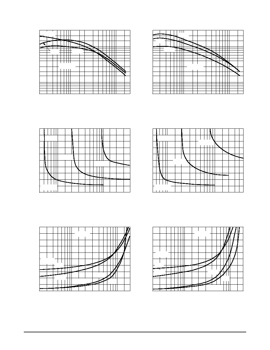
Figure 1. DC Current Gain
IC, COLLECTOR CURRENT (AMPS)
5.0
0.3
0.5 0.7 1.0
2.0
3.0
5.0
20
50
30
20
100
70
h
FE
, DC CURRENT
GAIN
150
°
C
25
°
C
55
°
C
VCE = 4 V
NPN
PNP
IC, COLLECTOR CURRENT (AMPS)
h
FE
, DC CURRENT
GAIN
7.0
10
200
7.0
10
Figure 2. DC Current Gain
150
°
C
25
°
C
55
°
C
Figure 3. Collector Saturation Region
2.0
0.05
IB, BASE CURRENT (AMPS)
0
0.07 0.1
0.2
0.3
0.5 0.7 1.0
2.0 3.0
1.6
1.2
0.8
0.4
TC = 25
°
C
IC = 4 A
IC = 16 A
Figure 4. Collector Saturation Region
2.0
IB, BASE CURRENT (AMPS)
0
1.6
1.2
0.8
0.4
TC = 25
°
C
2.0
0.2
IC, COLLECTOR CURRENT (AMPS)
0.3
0.5 0.7 1.0
2.0 3.0
5.0 7.0
20
1.2
0.4
0
IC/IB = 10
VBE(sat)
V
, VOL
T
AGE (VOL
TS)
Figure 5. "On" Voltage
1.6
0.8
10
150
°
C
25
°
C
VCE(sat)
25
°
C
2.0
IC, COLLECTOR CURRENT (AMPS)
1.2
0.4
IC/IB = 10
VBE(sat)
V
, VOL
T
AGE (VOL
TS)
Figure 6. "On" Voltage
1.6
0.8
150
°
C
25
°
C
VCE(sat)
150
°
C
25
°
C
VCE = 4 V
IC = 4 A
IC = 8 A
0.2 0.3
0.5 0.7 1.0
2.0
3.0
5.0
20
7.0
10
300
5.0
50
30
20
100
70
7.0
10
200
IC = 8 A
0.05 0.07 0.1
0.2
0.3
0.5 0.7
1.0
2.0 3.0
5.0
IC = 16 A
0.2 0.3
0.5 0.7 1.0
2.0 3.0
5.0 7.0
20
10
150
°
C
2N3773 2N6609
4
Motorola Bipolar Power Transistor Device Data
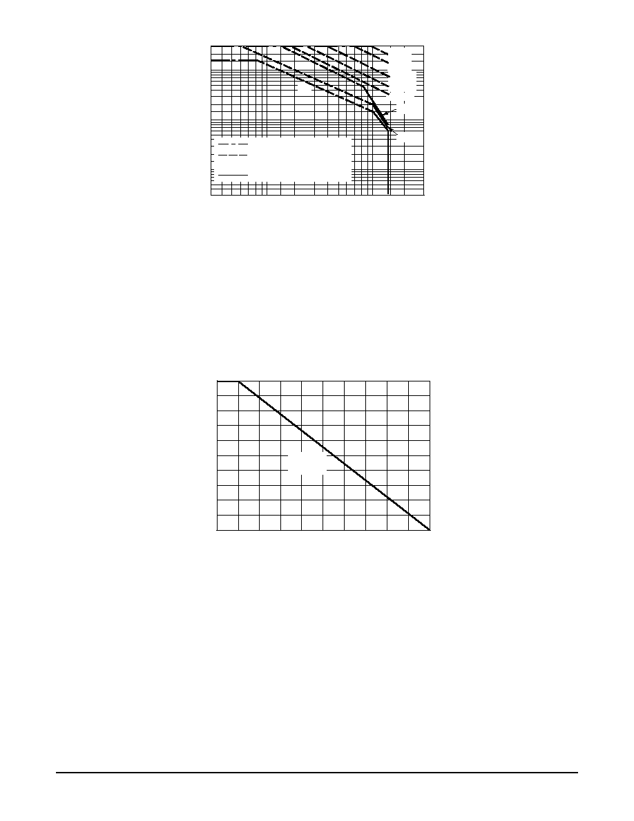
30
3.0
Figure 7. Forward Bias Safe Operating Area
VCE, COLLECTOREMITTER VOLTAGE (VOLTS)
20
10
5.0
3.0
2.0
1.0
0.5
0.03
5.0 7.0
10
20
30
50
300
BONDING WIRE LIMIT
THERMAL LIMIT
@ TC = 25
°
C, SINGLE PULSE
SECOND BREAKDOWN LIMIT
70
0.3
0.2
I C
, COLLECT
OR CURRENT
(AMP)
dc
10
µ
s
100
µ
s
100 ms
0.1
0.05
100
200
40
µ
s
200
µ
s
1.0 ms
500 ms
There are two limitations on the power handling ability of a
transistor: average junction temperature and second break-
down. Safe operating area curves indicate IC VCE limits of
the transistor that must be observed for reliable operation:
i.e., the transistor must not be subjected to greater dissipa-
tion than the curves indicate.
The data of Figure 7 is based on TJ(pk) = 200
_
C; TC is
variable depending on conditions. Second breakdown pulse
limits are valid for duty cycles to 10% provided TJ(pk)
< 200
_
C. At high case temperatures, thermal limitations will
reduce the power that can be handled to values less than the
limitations imposed by second breakdown.
100
80
60
40
0
20
0
40
80
120
160
200
Figure 8. Power Derating
TC, CASE TEMPERATURE (
°
C)
POWER DERA
TING F
ACT
OR (%)
THERMAL
DERATING
2N3773 2N6609
5
Motorola Bipolar Power Transistor Device Data
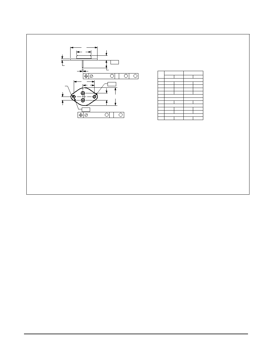
PACKAGE DIMENSIONS
NOTES:
1. DIMENSIONING AND TOLERANCING PER ANSI
Y14.5M, 1982.
2. CONTROLLING DIMENSION: INCH.
3. ALL RULES AND NOTES ASSOCIATED WITH
REFERENCED TO204AA OUTLINE SHALL APPLY.
STYLE 1:
PIN 1. BASE
2. EMITTER
CASE: COLLECTOR
DIM
MIN
MAX
MIN
MAX
MILLIMETERS
INCHES
A
1.550 REF
39.37 REF
B
1.050
26.67
C
0.250
0.335
6.35
8.51
D
0.038
0.043
0.97
1.09
E
0.055
0.070
1.40
1.77
G
0.430 BSC
10.92 BSC
H
0.215 BSC
5.46 BSC
K
0.440
0.480
11.18
12.19
L
0.665 BSC
16.89 BSC
N
0.830
21.08
Q
0.151
0.165
3.84
4.19
U
1.187 BSC
30.15 BSC
V
0.131
0.188
3.33
4.77
A
N
E
C
K
T
SEATING
PLANE
2 PL
D
M
Q
M
0.13 (0.005)
Y
M
T
M
Y
M
0.13 (0.005)
T
Q
Y
2
1
U
L
G
B
V
H
CASE 107
TO204AA (TO3)
ISSUE Z