 | ÐлекÑÑоннÑй компоненÑ: 2N4401ZL1 | СкаÑаÑÑ:  PDF PDF  ZIP ZIP |
Äîêóìåíòàöèÿ è îïèñàíèÿ www.docs.chipfind.ru
©
Semiconductor Components Industries, LLC, 2004
June, 2004 - Rev. 1
1
Publication Order Number:
2N4401/D
2N4401
Preferred Device
General Purpose
Transistors
NPN Silicon
Features
·
Pb-Free Packages are Available*
MAXIMUM RATINGS
Rating
Symbol
Value
Unit
Collector - Emitter Voltage
V
CEO
40
Vdc
Collector - Base Voltage
V
CBO
60
Vdc
Emitter - Base Voltage
V
EBO
6.0
Vdc
Collector Current - Continuous
I
C
600
mAdc
Total Device Dissipation
@ T
A
= 25
°
C
Derate above 25
°
C
P
D
625
5.0
mW
mW/
°
C
Total Device Dissipation
@ T
C
= 25
°
C
Derate above 25
°
C
P
D
1.5
12
W
mW/
°
C
Operating and Storage Junction
Temperature Range
T
J
, T
stg
-55 to +150
°
C
Maximum ratings are those values beyond which device damage can occur.
Maximum ratings applied to the device are individual stress limit values (not
normal operating conditions) and are not valid simultaneously. If these limits
are exceeded, device functional operation is not implied, damage may occur
and reliability may be affected.
THERMAL CHARACTERISTICS
Characteristic
Symbol
Max
Unit
Thermal Resistance,
Junction-to-Ambient
R
q
JA
200
°
C/W
Thermal Resistance,
Junction-to-Case
R
q
JC
83.3
°
C/W
*For additional information on our Pb-Free strategy and soldering details, please
download the ON Semiconductor Soldering and Mounting Techniques Reference
Manual, SOLDERRM/D.
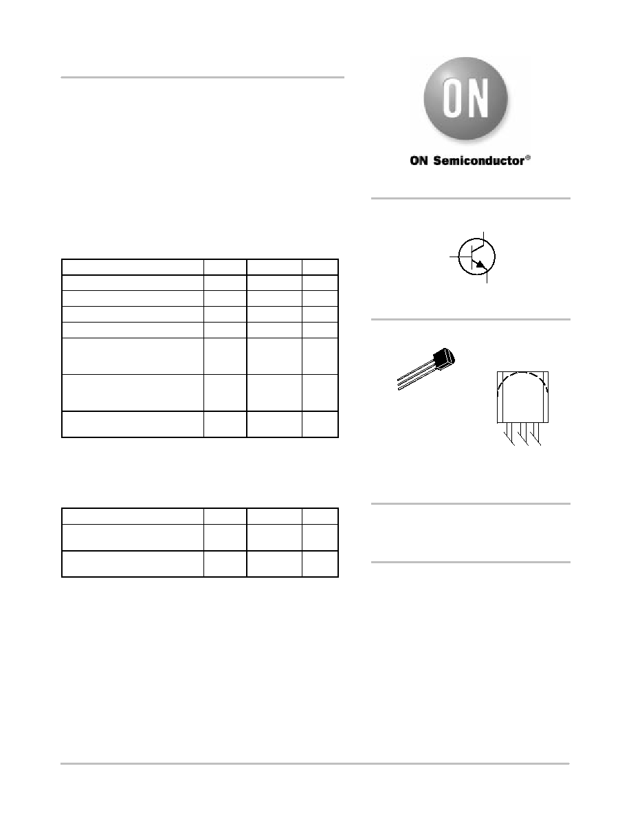
TO-92
CASE 29
STYLE 1
3
2
1
Preferred devices are recommended choices for future use
and best overall value.
Y
= Year
WW
= Work Week
MARKING
DIAGRAM
2N
4401
YWW
See detailed ordering and shipping information in the package
dimensions section on page 3 of this data sheet.
ORDERING INFORMATION
http://onsemi.com
COLLECTOR
3
2
BASE
1
EMITTER
2N4401
http://onsemi.com
2
ELECTRICAL CHARACTERISTICS
(T
A
= 25
°
C unless otherwise noted)
Characteristic
Symbol
Min
Max
Unit
OFF CHARACTERISTICS
Collector-Emitter Breakdown Voltage (Note 1)
(I
C
= 1.0 mAdc, I
B
= 0)
V
(BR)CEO
40
-
Vdc
Collector-Base Breakdown Voltage
(I
C
= 0.1 mAdc, I
E
= 0)
V
(BR)CBO
60
-
Vdc
Emitter-Base Breakdown Voltage
(I
E
= 0.1 mAdc, I
C
= 0)
V
(BR)EBO
6.0
-
Vdc
Base Cutoff Current
(V
CE
= 35 Vdc, V
EB
= 0.4 Vdc)
I
BEV
-
0.1
m
Adc
Collector Cutoff Current
(V
CE
= 35 Vdc, V
EB
= 0.4 Vdc)
I
CEX
-
0.1
m
Adc
ON CHARACTERISTICS (Note 1)
DC Current Gain
(I
C
= 0.1 mAdc, V
CE
= 1.0 Vdc)
(I
C
= 1.0 mAdc, V
CE
= 1.0 Vdc)
(I
C
= 10 mAdc, V
CE
= 1.0 Vdc)
(I
C
= 150 mAdc, V
CE
= 1.0 Vdc)
(I
C
= 500 mAdc, V
CE
= 2.0 Vdc)
h
FE
20
40
80
100
40
-
-
-
300
-
-
Collector-Emitter Saturation Voltage (I
C
= 150 mAdc, I
B
= 15 mAdc)
Collector-Emitter Saturation Voltage
(I
C
= 500 mAdc, I
B
= 50 mAdc)
V
CE(sat)
-
-
0.4
0.75
Vdc
Base-Emitter Saturation Voltage (I
C
= 150 mAdc, I
B
= 15 mAdc)
Base-Emitter Saturation Voltage
(I
C
= 500 mAdc, I
B
= 50 mAdc)
V
BE(sat)
0.75
-
0.95
1.2
Vdc
SMALL-SIGNAL CHARACTERISTICS
Current-Gain - Bandwidth Product (I
C
= 20 mAdc, V
CE
= 10 Vdc, f = 100 MHz)
f
T
250
-
MHz
Collector-Base Capacitance (V
CB
= 5.0 Vdc, I
E
= 0, f = 1.0 MHz)
C
cb
-
6.5
pF
Emitter-Base Capacitance (V
EB
= 0.5 Vdc, I
C
= 0, f = 1.0 MHz)
C
eb
-
30
pF
Input Impedance (I
C
= 1.0 mAdc, V
CE
= 10 Vdc, f = 1.0 kHz)
h
ie
1.0
15
k ohms
Voltage Feedback Ratio (I
C
= 1.0 mAdc, V
CE
= 10 Vdc, f = 1.0 kHz)
h
re
0.1
8.0
X 10
-4
Small-Signal Current Gain (I
C
= 1.0 mAdc, V
CE
= 10 Vdc, f = 1.0 kHz)
h
fe
40
500
-
Output Admittance (I
C
= 1.0 mAdc, V
CE
= 10 Vdc, f = 1.0 kHz)
h
oe
1.0
30
m
mhos
SWITCHING CHARACTERISTICS
Delay Time
(V
CC
= 30 Vdc, V
BE
= 2.0 Vdc,
t
d
-
15
ns
Rise Time
(V
CC
30 Vdc, V
BE
2.0 Vdc,
I
C
= 150 mAdc, I
B1
= 15 mAdc)
t
r
-
20
ns
Storage Time
(V
CC
= 30 Vdc, I
C
= 150 mAdc,
t
s
-
225
ns
Fall Time
(V
CC
30 Vdc, I
C
150 mAdc,
I
B1
= I
B2
= 15 mAdc)
t
f
-
30
ns
1. Pulse Test: Pulse Width
300
m
s, Duty Cycle
2.0%.
2N4401
http://onsemi.com
3
ORDERING INFORMATION
Device
Package
Shipping
2N4401
TO-92
5,000 Units / Box
2N4401RLRA
TO-92
2,000 / Tape & Reel
2N4401RLRAG
TO-92
(Pb-Free)
2,000 / Tape & Reel
2N4401RLRM
TO-92
2,000 / Ammo Pack
2N4401RLRP
TO-92
2,000 / Ammo Pack
2N4401RLRPG
TO-92
(Pb-Free)
2,000 / Ammo Pack
2N4401ZL1
TO-92
2,000 / Ammo Pack
For information on tape and reel specifications, including part orientation and tape sizes, please refer to our Tape and Reel Packaging
Specifications Brochure, BRD8011/D.
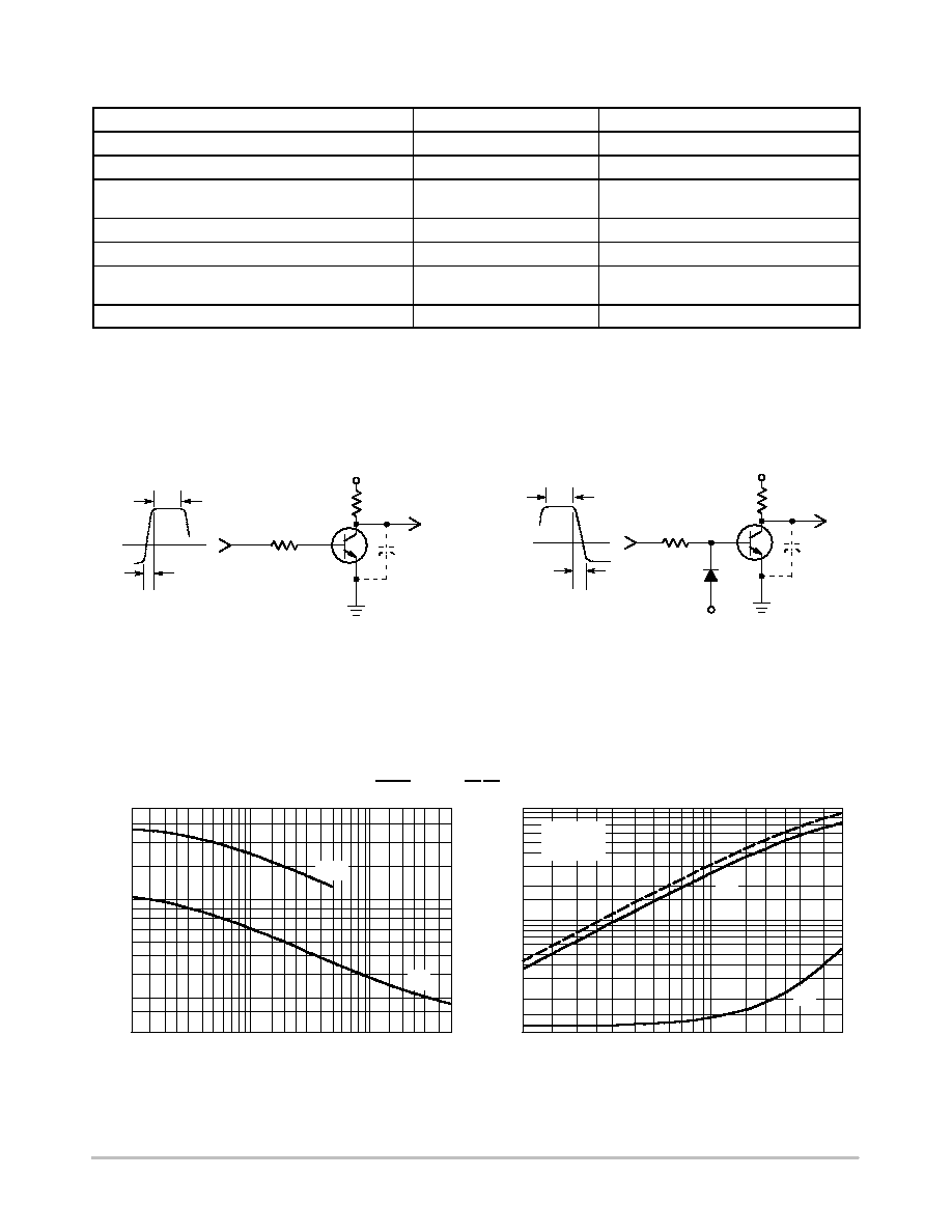
Figure 1. Turn-On Time
Figure 2. Turn-Off Time
SWITCHING TIME EQUIVALENT TEST CIRCUITS
Scope rise time < 4.0 ns
*Total shunt capacitance of test jig connectors, and oscilloscope
+16 V
-2.0 V
< 2.0 ns
0
1.0 to 100 ms,
DUTY CYCLE
2.0%
1.0 kW
+30 V
200 W
C
S
* < 10 pF
+16 V
-14 V
0
< 20 ns
1.0 to 100 ms,
DUTY CYCLE
2.0%
1.0 kW
+30 V
200 W
C
S
* < 10 pF
-4.0 V
Figure 3. Capacitances
REVERSE VOLTAGE (VOLTS)
7.0
10
20
30
5.0
Figure 4. Charge Data
I
C
, COLLECTOR CURRENT (mA)
0.1
2.0
5.0
10
20
2.0
30
50
CAP
ACIT
ANCE (pF)
Q, CHARGE (nC)
3.0
2.0
3.0
5.0
7.0
10
1.0
10
20
50
70
100
200
0.1
300
500
0.7
0.5
V
CC
= 30 V
I
C
/I
B
= 10
C
obo
Q
T
Q
A
25
°
C
100
°
C
TRANSIENT CHARACTERISTICS
3.0
1.0
0.5
0.3
0.2
0.3
0.2
30
C
cb
2N4401
http://onsemi.com
4
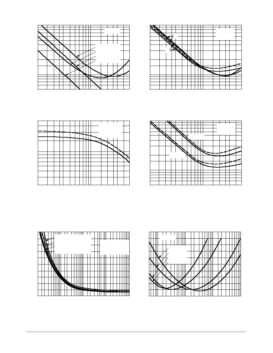
Figure 5. Turn-On Time
I
C
, COLLECTOR CURRENT (mA)
20
30
50
5.0
10
7.0
Figure 6. Rise and Fall Times
I
C
, COLLECTOR CURRENT (mA)
Figure 7. Storage Time
I
C
, COLLECTOR CURRENT (mA)
Figure 8. Fall Time
I
C
, COLLECTOR CURRENT (mA)
20
30
50
70
100
10
5.0
7.0
t s
, STORAGE TIME (ns)
t, TIME (ns)
t, TIME (ns)
t f
, FALL
TIME (ns)
70
100
10
20
50
70
100
200
300
500
30
I
C
/I
B
= 10
t
r
@ V
CC
= 30 V
t
r
@ V
CC
= 10 V
t
d
@ V
EB
= 2.0 V
t
d
@ V
EB
= 0
20
30
50
5.0
10
7.0
70
100
10
20
50
70 100
200
300
500
30
V
CC
= 30 V
I
C
/I
B
= 10
t
r
t
f
10
20
50
70
100
200
300
500
30
100
200
30
70
50
300
10
20
50
70
100
200
300
500
30
t
s
= t
s
- 1/8 t
f
I
B1
= I
B2
I
C
/I
B
= 10 to 20
V
CC
= 30 V
I
B1
= I
B2
I
C
/I
B
= 20
I
C
/I
B
= 10
6.0
8.0
10
0
4.0
2.0
0.1
2.0 5.0
10
20
50
1.0
0.5
0.2
0.01 0.02 0.05
100
Figure 9. Frequency Effects
f, FREQUENCY (kHz)
SMALL-SIGNAL CHARACTERISTICS
NOISE FIGURE
V
CE
= 10 Vdc, T
A
= 25
°
C; Bandwidth = 1.0 Hz
NF
, NOISE FIGURE (dB)
I
C
= 1.0 mA, R
S
= 150 W
I
C
= 500 mA, R
S
= 200 W
I
C
= 100 mA, R
S
= 2.0 kW
I
C
= 50 mA, R
S
= 4.0 kW
R
S
= OPTIMUM
RS =
SOURCE
RS =
RESISTANCE
100 k
50
100 200
500 1.0 k 2.0 k
5.0 k 10 k 20 k
50 k
6.0
8.0
10
0
4.0
2.0
NF
, NOISE FIGURE (dB)
Figure 10. Source Resistance Effects
R
S
, SOURCE RESISTANCE (OHMS)
f = 1.0 kHz
I
C
= 50 mA
I
C
= 100 mA
I
C
= 500 mA
I
C
= 1.0 mA
2N4401
http://onsemi.com
5
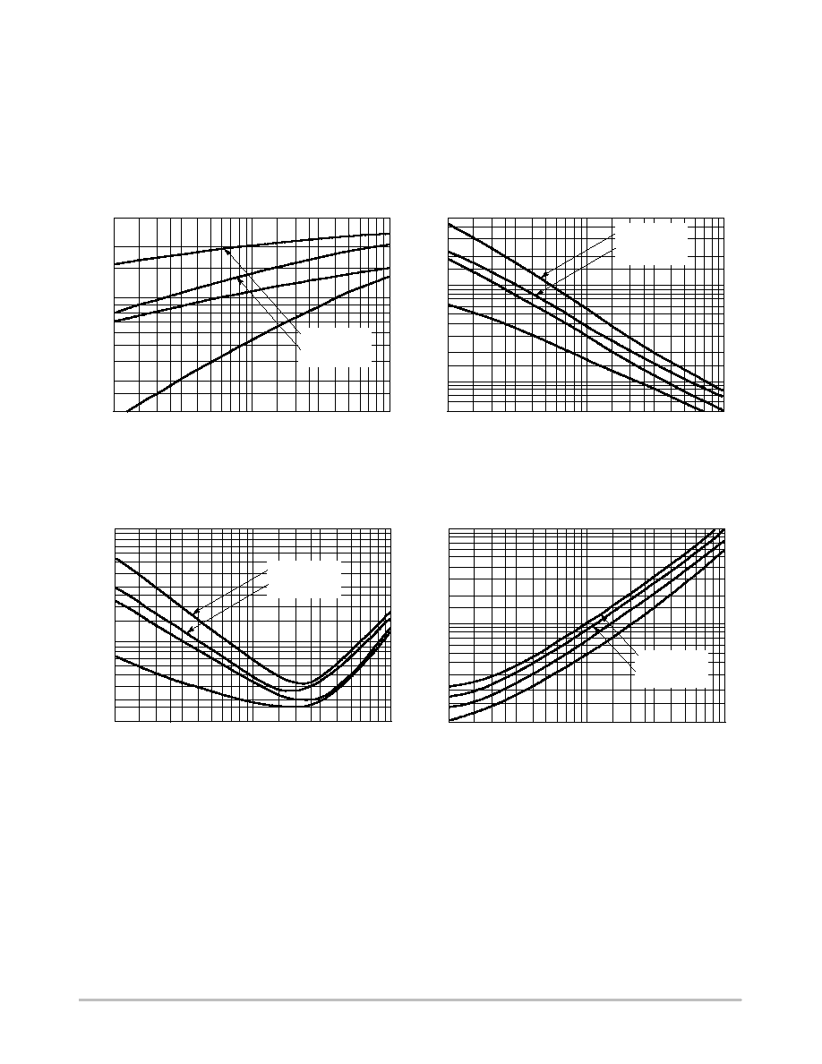
h PARAMETERS
V
CE
= 10 Vdc, f = 1.0 kHz, T
A
= 25
°
C
This group of graphs illustrates the relationship between
h
fe
and other "h" parameters for this series of transistors. To
obtain these curves, a high-gain and a low-gain unit were
selected from the 2N4401 lines, and the same units were
used to develop the correspondingly numbered curves on
each graph.
Figure 11. Current Gain
I
C
, COLLECTOR CURRENT (mA)
0.1
0.2
0.5 0.7 1.0
2.0 3.0
10
0.3
100
200
20
70
50
300
h fe
, CURRENT GAIN
h ie
, INPUT IMPEDANCE (OHMS)
Figure 12. Input Impedance
I
C
, COLLECTOR CURRENT (mA)
50 k
500
30
5.0 7.0
20 k
10 k
5.0 k
2.0 k
1.0 k
0.1
0.2
0.5 0.7 1.0
2.0 3.0
10
0.3
5.0 7.0
Figure 13. Voltage Feedback Ratio
I
C
, COLLECTOR CURRENT (mA)
0.1
0.2
0.5 0.7 1.0
2.0
3.0
10
0.3
0.2
10
Figure 14. Output Admittance
I
C
, COLLECTOR CURRENT (mA)
100
1.0
5.0 7.0
50
20
10
5.0
2.0
7.0
5.0
3.0
2.0
1.0
0.7
0.5
0.3
h , OUTPUT
ADMITT
ANCE ( mhos)
oe
h , VOL
T
AGE FEEDBACK RA
TIO (X 10 )
re
m
-4
2N4401 UNIT 1
2N4401 UNIT 2
2N4401 UNIT 1
2N4401 UNIT 2
2N4401 UNIT 1
2N4401 UNIT 2
2N4401 UNIT 1
2N4401 UNIT 2
0.1
0.2
0.5 0.7 1.0
2.0 3.0
10
0.3
5.0 7.0