 | –≠–ª–µ–∫—Ç—Ä–æ–Ω–Ω—ã–π –∫–æ–º–ø–æ–Ω–µ–Ω—Ç: 2N4918 | –°–∫–∞—á–∞—Ç—å:  PDF PDF  ZIP ZIP |

Medium-Power Plastic PNP
Silicon Transistors
. . . designed for driver circuits, switching, and amplifier
applications. These high≠performance plastic devices feature:
∑
Low Saturation Voltage --
VCE(sat) = 0.6 Vdc (Max) @ IC = 1.0 Amp
∑
Excellent Power Dissipation Due to Thermopad Construction --
PD = 30 W @ TC = 25_C
∑
Excellent Safe Operating Area
∑
Gain Specified to IC = 1.0 Amp
∑
Complement to NPN 2N4921, 2N4922, 2N4923
ŒŒŒŒŒŒŒŒŒŒŒŒŒŒŒŒŒŒŒŒŒŒŒ
Œ
ŒŒŒŒŒŒŒŒŒŒŒŒŒŒŒŒŒŒŒŒŒ
Œ
ŒŒŒŒŒŒŒŒŒŒŒŒŒŒŒŒŒŒŒŒŒŒŒ
*MAXIMUM RATINGS
ŒŒŒŒŒŒŒŒŒŒŒ
ŒŒŒŒŒŒŒŒŒŒŒ
Ratings
ŒŒŒ
ŒŒŒ
Symbol
ŒŒŒŒ
ŒŒŒŒ
2N4918
ŒŒŒ
ŒŒŒ
2N4919
ŒŒŒŒ
ŒŒŒŒ
2N4920
ŒŒŒ
ŒŒŒ
Unit
ŒŒŒŒŒŒŒŒŒŒŒ
ŒŒŒŒŒŒŒŒŒŒŒ
Collector≠Emitter Voltage
ŒŒŒ
ŒŒŒ
VCEO
ŒŒŒŒ
ŒŒŒŒ
40
ŒŒŒ
ŒŒŒ
60
ŒŒŒŒ
ŒŒŒŒ
80
ŒŒŒ
ŒŒŒ
Vdc
ŒŒŒŒŒŒŒŒŒŒŒ
ŒŒŒŒŒŒŒŒŒŒŒ
Collector≠Base Voltage
ŒŒŒ
ŒŒŒ
VCB
ŒŒŒŒ
ŒŒŒŒ
40
ŒŒŒ
ŒŒŒ
60
ŒŒŒŒ
ŒŒŒŒ
80
ŒŒŒ
ŒŒŒ
Vdc
ŒŒŒŒŒŒŒŒŒŒŒ
ŒŒŒŒŒŒŒŒŒŒŒ
Emitter≠Base Voltage
ŒŒŒ
ŒŒŒ
VEB
ŒŒŒŒŒŒŒŒŒ
ŒŒŒŒŒŒŒŒŒ
5.0
ŒŒŒ
ŒŒŒ
Vdc
ŒŒŒŒŒŒŒŒŒŒŒ
Œ
ŒŒŒŒŒŒŒŒŒ
Œ
ŒŒŒŒŒŒŒŒŒŒŒ
Collector Current -- Continuous (1)
ŒŒŒ
Œ
Œ
Œ
ŒŒŒ
IC*
ŒŒŒŒŒŒŒŒŒ
Œ
ŒŒŒŒŒŒŒ
Œ
ŒŒŒŒŒŒŒŒŒ
1.0
3.0
ŒŒŒ
Œ
Œ
Œ
ŒŒŒ
Adc
ŒŒŒŒŒŒŒŒŒŒŒ
ŒŒŒŒŒŒŒŒŒŒŒ
Base Current
ŒŒŒ
ŒŒŒ
IB
ŒŒŒŒŒŒŒŒŒ
ŒŒŒŒŒŒŒŒŒ
1.0
ŒŒŒ
ŒŒŒ
Adc
ŒŒŒŒŒŒŒŒŒŒŒ
Œ
ŒŒŒŒŒŒŒŒŒ
Œ
ŒŒŒŒŒŒŒŒŒŒŒ
Total Power Dissipation @ TC = 25
∞
C
Derate above 25
_
C
ŒŒŒ
Œ
Œ
Œ
ŒŒŒ
PD
ŒŒŒŒŒŒŒŒŒ
Œ
ŒŒŒŒŒŒŒ
Œ
ŒŒŒŒŒŒŒŒŒ
30
0.24
ŒŒŒ
Œ
Œ
Œ
ŒŒŒ
Watts
W/
_
C
ŒŒŒŒŒŒŒŒŒŒŒ
ŒŒŒŒŒŒŒŒŒŒŒ
Operating & Storage Junction
Temperature Range
ŒŒŒ
ŒŒŒ
TJ, Tstg
ŒŒŒŒŒŒŒŒŒ
ŒŒŒŒŒŒŒŒŒ
≠65 to +150
ŒŒŒ
ŒŒŒ
_
C
ŒŒŒŒŒŒŒŒŒŒŒŒŒŒŒŒŒŒŒŒŒŒŒ
Œ
ŒŒŒŒŒŒŒŒŒŒŒŒŒŒŒŒŒŒŒŒŒ
Œ
ŒŒŒŒŒŒŒŒŒŒŒŒŒŒŒŒŒŒŒŒŒŒŒ
THERMAL CHARACTERISTICS (2)
ŒŒŒŒŒŒŒŒŒŒŒŒ
ŒŒŒŒŒŒŒŒŒŒŒŒ
Characteristic
ŒŒŒŒŒ
ŒŒŒŒŒ
Symbol
ŒŒŒŒŒŒ
ŒŒŒŒŒŒ
Max
ŒŒŒ
ŒŒŒ
Unit
ŒŒŒŒŒŒŒŒŒŒŒŒ
ŒŒŒŒŒŒŒŒŒŒŒŒ
Thermal Resistance, Junction to Case
ŒŒŒŒŒ
ŒŒŒŒŒ
JC
ŒŒŒŒŒŒ
ŒŒŒŒŒŒ
4.16
ŒŒŒ
ŒŒŒ
_
C/W
*Indicates JEDEC Registered Data for 2N4918 Series.
(1) The 1.0 Amp maximum IC value is based upon JEDEC current gain requirements.
The 3.0 Amp maximum value is based upon actual current≠handling capability of the
device (See Figure 5).
(2) Recommend use of thermal compound for lowest thermal resistance.
Preferred devices are ON Semiconductor recommended choices for future use and best overall value.
ON Semiconductor
)
©
Semiconductor Components Industries, LLC, 2002
April, 2002 ≠ Rev. 10
1
Publication Order Number:
2N4918/D
2N4918
thru
2N4920
*ON Semiconductor Preferred Device
3 AMPERE
GENERAL≠PURPOSE
POWER TRANSISTORS
40≠80 VOLTS
30 WATTS
*
CASE 77≠09
TO≠225AA TYPE
3
2 1
STYLE 1:
PIN 1. EMITTER
2. COLLECTOR
3. BASE
2N4918 thru 2N4920
http://onsemi.com
2
40
30
20
10
0
25
50
75
100
125
150
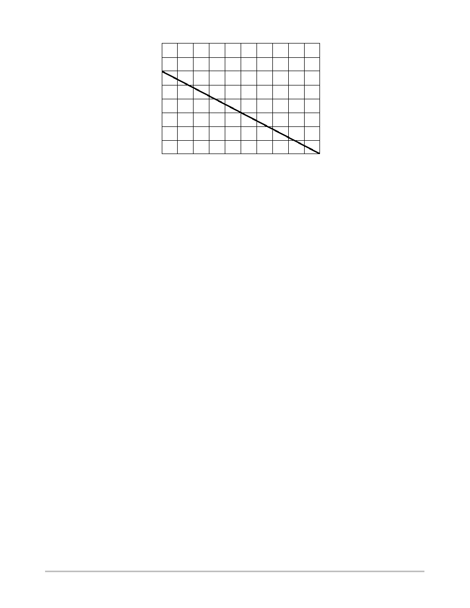
Figure 1. Power Derating
TC, CASE TEMPERATURE (
∞
C)
P D
, POWER DISSIP
A
TION (W
A
TTS)

2N4918 thru 2N4920
http://onsemi.com
3
ŒŒŒŒŒŒŒŒŒŒŒŒŒŒŒŒŒŒŒŒŒŒŒŒŒŒŒŒŒŒŒŒŒ
ŒŒŒŒŒŒŒŒŒŒŒŒŒŒŒŒŒŒŒŒŒŒŒŒŒŒŒŒŒŒŒŒŒ
ELECTRICAL CHARACTERISTICS
(TC = 25
_
C unless otherwise noted)
ŒŒŒŒŒŒŒŒŒŒŒŒŒŒŒŒŒŒŒŒŒŒ
ŒŒŒŒŒŒŒŒŒŒŒŒŒŒŒŒŒŒŒŒŒŒ
Characteristic
ŒŒŒŒŒ
ŒŒŒŒŒ
Symbol
ŒŒŒ
ŒŒŒ
Min
ŒŒŒŒ
ŒŒŒŒ
Max
ŒŒŒ
ŒŒŒ
Unit
ŒŒŒŒŒŒŒŒŒŒŒŒŒŒŒŒŒŒŒŒŒŒŒŒŒŒŒŒŒŒŒŒŒ
ŒŒŒŒŒŒŒŒŒŒŒŒŒŒŒŒŒŒŒŒŒŒŒŒŒŒŒŒŒŒŒŒŒ
OFF CHARACTERISTICS
ŒŒŒŒŒŒŒŒŒŒŒŒŒŒŒŒŒŒŒŒŒŒ
Œ
ŒŒŒŒŒŒŒŒŒŒŒŒŒŒŒŒŒŒŒŒ
Œ
Œ
ŒŒŒŒŒŒŒŒŒŒŒŒŒŒŒŒŒŒŒŒ
Œ
ŒŒŒŒŒŒŒŒŒŒŒŒŒŒŒŒŒŒŒŒŒŒ
Collector≠Emitter Sustaining Voltage (1)
(IC = 0.1 Adc, IB = 0)
2N4918
2N4919
2N4920
ŒŒŒŒŒ
Œ
ŒŒŒ
Œ
Œ
ŒŒŒ
Œ
ŒŒŒŒŒ
VCEO(sus)
ŒŒŒ
Œ
Œ
Œ
Œ
Œ
Œ
ŒŒŒ
40
60
80
ŒŒŒŒ
Œ
ŒŒ
Œ
Œ
ŒŒ
Œ
ŒŒŒŒ
--
--
--
ŒŒŒ
Œ
Œ
Œ
Œ
Œ
Œ
ŒŒŒ
Vdc
ŒŒŒŒŒŒŒŒŒŒŒŒŒŒŒŒŒŒŒŒŒŒ
Œ
ŒŒŒŒŒŒŒŒŒŒŒŒŒŒŒŒŒŒŒŒ
Œ
Œ
ŒŒŒŒŒŒŒŒŒŒŒŒŒŒŒŒŒŒŒŒ
Œ
ŒŒŒŒŒŒŒŒŒŒŒŒŒŒŒŒŒŒŒŒŒŒ
Collector Cutoff Current
(VCE = 20 Vdc, IB = 0)
2N4918
(VCE = 30 Vdc, IB = 0)
2N4919
(VCE = 40 Vdc, IB = 0)
2N4920
ŒŒŒŒŒ
Œ
ŒŒŒ
Œ
Œ
ŒŒŒ
Œ
ŒŒŒŒŒ
ICEO
ŒŒŒ
Œ
Œ
Œ
Œ
Œ
Œ
ŒŒŒ
--
--
--
ŒŒŒŒ
Œ
ŒŒ
Œ
Œ
ŒŒ
Œ
ŒŒŒŒ
0.5
0.5
0.5
ŒŒŒ
Œ
Œ
Œ
Œ
Œ
Œ
ŒŒŒ
mAdc
ŒŒŒŒŒŒŒŒŒŒŒŒŒŒŒŒŒŒŒŒŒŒ
Œ
ŒŒŒŒŒŒŒŒŒŒŒŒŒŒŒŒŒŒŒŒ
Œ
Œ
ŒŒŒŒŒŒŒŒŒŒŒŒŒŒŒŒŒŒŒŒ
Œ
ŒŒŒŒŒŒŒŒŒŒŒŒŒŒŒŒŒŒŒŒŒŒ
Collector Cutoff Current
(VCE = Rated VCEO, VBE(off) = 1.5 Vdc)
(VCE = Rated VCEO, VBE(off) = 1.5 Vdc, TC = 125
_
C
ŒŒŒŒŒ
Œ
ŒŒŒ
Œ
Œ
ŒŒŒ
Œ
ŒŒŒŒŒ
ICEX
ŒŒŒ
Œ
Œ
Œ
Œ
Œ
Œ
ŒŒŒ
--
--
ŒŒŒŒ
Œ
ŒŒ
Œ
Œ
ŒŒ
Œ
ŒŒŒŒ
0.1
0.5
ŒŒŒ
Œ
Œ
Œ
Œ
Œ
Œ
ŒŒŒ
mAdc
ŒŒŒŒŒŒŒŒŒŒŒŒŒŒŒŒŒŒŒŒŒŒ
ŒŒŒŒŒŒŒŒŒŒŒŒŒŒŒŒŒŒŒŒŒŒ
Collector Cutoff Current
(VCB = Rated VCB, IE = 0)
ŒŒŒŒŒ
ŒŒŒŒŒ
ICBO
ŒŒŒ
ŒŒŒ
--
ŒŒŒŒ
ŒŒŒŒ
0.1
ŒŒŒ
ŒŒŒ
mAdc
ŒŒŒŒŒŒŒŒŒŒŒŒŒŒŒŒŒŒŒŒŒŒ
Œ
ŒŒŒŒŒŒŒŒŒŒŒŒŒŒŒŒŒŒŒŒ
Œ
ŒŒŒŒŒŒŒŒŒŒŒŒŒŒŒŒŒŒŒŒŒŒ
Emitter Cutoff Current
(VBE = 5.0 Vdc, IC = 0)
ŒŒŒŒŒ
Œ
ŒŒŒ
Œ
ŒŒŒŒŒ
IEBO
ŒŒŒ
Œ
Œ
Œ
ŒŒŒ
--
ŒŒŒŒ
Œ
ŒŒ
Œ
ŒŒŒŒ
1.0
ŒŒŒ
Œ
Œ
Œ
ŒŒŒ
mAdc
ŒŒŒŒŒŒŒŒŒŒŒŒŒŒŒŒŒŒŒŒŒŒŒŒŒŒŒŒŒŒŒŒŒ
ŒŒŒŒŒŒŒŒŒŒŒŒŒŒŒŒŒŒŒŒŒŒŒŒŒŒŒŒŒŒŒŒŒ
ON CHARACTERISTICS
ŒŒŒŒŒŒŒŒŒŒŒŒŒŒŒŒŒŒŒŒŒŒ
Œ
ŒŒŒŒŒŒŒŒŒŒŒŒŒŒŒŒŒŒŒŒ
Œ
Œ
ŒŒŒŒŒŒŒŒŒŒŒŒŒŒŒŒŒŒŒŒ
Œ
ŒŒŒŒŒŒŒŒŒŒŒŒŒŒŒŒŒŒŒŒŒŒ
DC Current Gain (1)
(IC = 50 mAdc, VCE = 1.0 Vdc)
(IC = 500 mAdc, VCE = 1.0 Vdc)
(IC = 1.0 Adc, VCE = 1.0 Vdc)
ŒŒŒŒŒ
Œ
ŒŒŒ
Œ
Œ
ŒŒŒ
Œ
ŒŒŒŒŒ
hFE
ŒŒŒ
Œ
Œ
Œ
Œ
Œ
Œ
ŒŒŒ
40
30
10
ŒŒŒŒ
Œ
ŒŒ
Œ
Œ
ŒŒ
Œ
ŒŒŒŒ
--
150
--
ŒŒŒ
Œ
Œ
Œ
Œ
Œ
Œ
ŒŒŒ
--
ŒŒŒŒŒŒŒŒŒŒŒŒŒŒŒŒŒŒŒŒŒŒ
Œ
ŒŒŒŒŒŒŒŒŒŒŒŒŒŒŒŒŒŒŒŒ
Œ
ŒŒŒŒŒŒŒŒŒŒŒŒŒŒŒŒŒŒŒŒŒŒ
Collector≠Emitter Saturation Voltage (1)
(IC = 1.0 Adc, IB = 0.1 Adc)
ŒŒŒŒŒ
Œ
ŒŒŒ
Œ
ŒŒŒŒŒ
VCE(sat)
ŒŒŒ
Œ
Œ
Œ
ŒŒŒ
--
ŒŒŒŒ
Œ
ŒŒ
Œ
ŒŒŒŒ
0.6
ŒŒŒ
Œ
Œ
Œ
ŒŒŒ
Vdc
ŒŒŒŒŒŒŒŒŒŒŒŒŒŒŒŒŒŒŒŒŒŒ
ŒŒŒŒŒŒŒŒŒŒŒŒŒŒŒŒŒŒŒŒŒŒ
Base≠Emitter Saturation Voltage (1)
(IC = 1.0 Adc, IB = 0.1 Adc)
ŒŒŒŒŒ
ŒŒŒŒŒ
VBE(sat)
ŒŒŒ
ŒŒŒ
--
ŒŒŒŒ
ŒŒŒŒ
1.3
ŒŒŒ
ŒŒŒ
Vdc
ŒŒŒŒŒŒŒŒŒŒŒŒŒŒŒŒŒŒŒŒŒŒ
Œ
ŒŒŒŒŒŒŒŒŒŒŒŒŒŒŒŒŒŒŒŒ
Œ
ŒŒŒŒŒŒŒŒŒŒŒŒŒŒŒŒŒŒŒŒŒŒ
Base≠Emitter On Voltage (1)
(IC = 1.0 Adc, VCE = 1.0 Vdc)
ŒŒŒŒŒ
Œ
ŒŒŒ
Œ
ŒŒŒŒŒ
VBE(on)
ŒŒŒ
Œ
Œ
Œ
ŒŒŒ
--
ŒŒŒŒ
Œ
ŒŒ
Œ
ŒŒŒŒ
1.3
ŒŒŒ
Œ
Œ
Œ
ŒŒŒ
Vdc
ŒŒŒŒŒŒŒŒŒŒŒŒŒŒŒŒŒŒŒŒŒŒŒŒŒŒŒŒŒŒŒŒŒ
ŒŒŒŒŒŒŒŒŒŒŒŒŒŒŒŒŒŒŒŒŒŒŒŒŒŒŒŒŒŒŒŒŒ
SMALL≠SIGNAL CHARACTERISTICS
ŒŒŒŒŒŒŒŒŒŒŒŒŒŒŒŒŒŒŒŒŒŒ
ŒŒŒŒŒŒŒŒŒŒŒŒŒŒŒŒŒŒŒŒŒŒ
Current≠Gain -- Bandwidth Product (IC = 250 mAdc, VCE = 10 Vdc, f = 1.0 MHz)
ŒŒŒŒŒ
ŒŒŒŒŒ
fT
ŒŒŒ
ŒŒŒ
3.0
ŒŒŒŒ
ŒŒŒŒ
--
ŒŒŒ
ŒŒŒ
MHz
ŒŒŒŒŒŒŒŒŒŒŒŒŒŒŒŒŒŒŒŒŒŒ
ŒŒŒŒŒŒŒŒŒŒŒŒŒŒŒŒŒŒŒŒŒŒ
Output Capacitance (VCB = 10 Vdc, IE = 0, f = 100 kHz)
ŒŒŒŒŒ
ŒŒŒŒŒ
Cob
ŒŒŒ
ŒŒŒ
--
ŒŒŒŒ
ŒŒŒŒ
100
ŒŒŒ
ŒŒŒ
pF
ŒŒŒŒŒŒŒŒŒŒŒŒŒŒŒŒŒŒŒŒŒŒ
ŒŒŒŒŒŒŒŒŒŒŒŒŒŒŒŒŒŒŒŒŒŒ
Small≠Signal Current Gain (IC = 250 mAdc, VCE = 10 Vdc, f = 1.0 kHz)
ŒŒŒŒŒ
ŒŒŒŒŒ
hfe
ŒŒŒ
ŒŒŒ
25
ŒŒŒŒ
ŒŒŒŒ
--
ŒŒŒ
ŒŒŒ
--
*Indicates JEDEC Registered Data.
(1) Pulse Test: PW
[
300
µ
s, Duty Cycle
[
2.0%
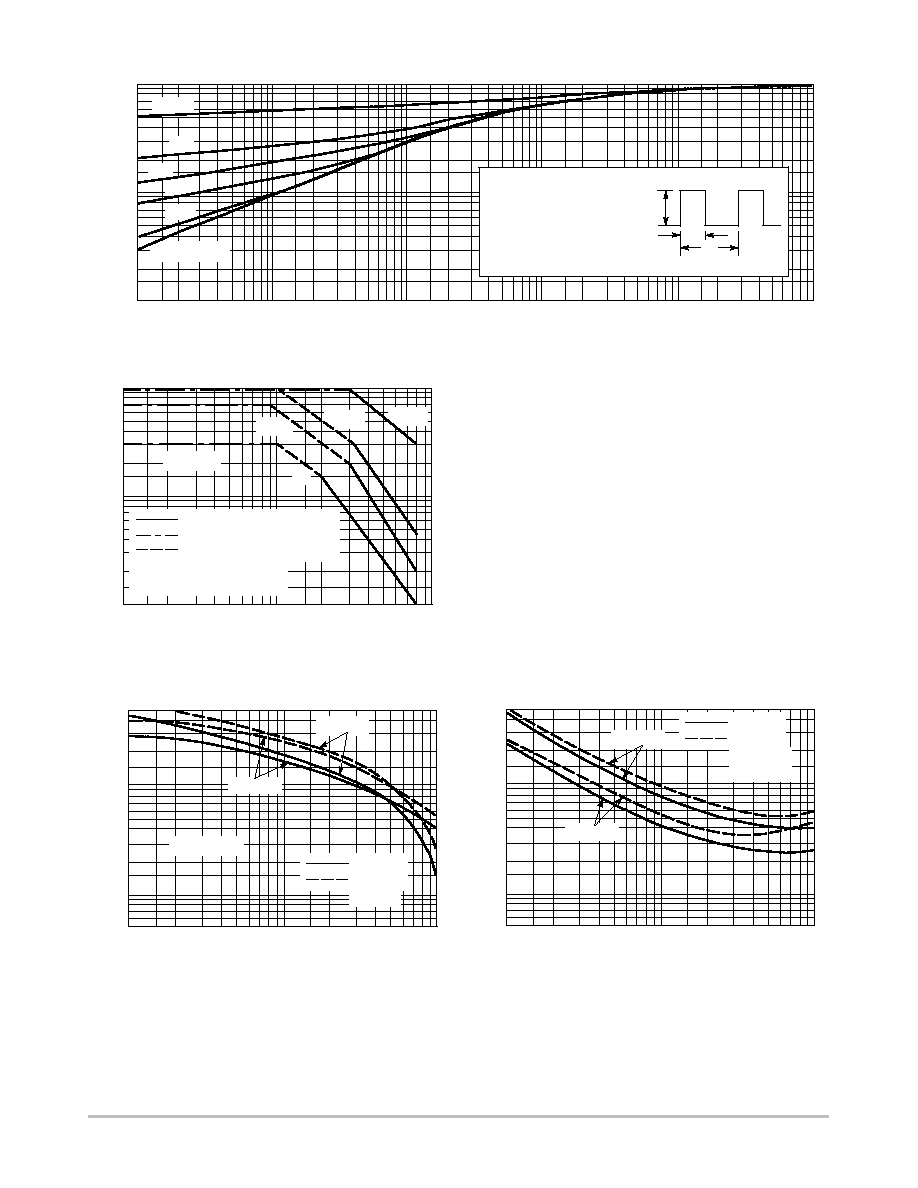
Figure 2. Switching Time Equivalent Test Circuit
5.0
10
Figure 3. Turn≠On Time
IC, COLLECTOR CURRENT (mA)
VCC = 30 V
IC/IB = 20
t, TIME
(s)
µ
2.0
1.0
0.7
0.5
0.3
0.2
0.1
0.05
20 30
50 70 100
200
700 1000
Vin
t1
VBE(off)
APPROX 9.0 V
TURN-OFF PULSE
t3
t2
APPROX
-11 V
VCC
SCOPE
RB
Cjd << Ceb
+4.0 V
t1 < 15 ns
100 < t2 < 500
µ
s
t3 < 15 ns
DUTY CYCLE
2.0%
Vin
RC
0.07
3.0
TJ = 25
∞
C
TJ = 150
∞
C
IC/IB = 10, UNLESS NOTED
VCC = 60 V
VCC = 30 V
VCC = 30 V
VBE(off) = 0
300
500
0
0
Vin
APPROX
-11 V
RB and RC
varied to
obtain desired
current levels
tr
VBE(off) = 2.0 V
VCC = 60 V
td
2N4918 thru 2N4920
http://onsemi.com
4
Figure 4. Thermal Response
t, TIME (ms)
1.0
0.01
0.01
0.7
0.5
0.3
0.2
0.1
0.07
0.05
0.03
0.02
0.02 0.03
r(t)
, TRANSIENT
THERMAL
RESIST
ANCE
(NORMALIZED)
0.05
0.1
0.2 0.3
0.5
1.0
2.0 3.0
5.0
10
20 30
50
100
200 300
1000
500
JC(t) = r(t)
JC
JC = 4.16
∞
C/W MAX
D CURVES APPLY FOR POWER
PULSE TRAIN SHOWN
READ TIME AT t1
TJ(pk) - TC = P(pk)
JC(t)
P(pk)
t1
t2
DUTY CYCLE, D = t1/t2
D = 0.5
0.2
0.05
0.01
SINGLE PULSE
0.1
10
1.0
Figure 5. Active≠Region Safe Operating Area
VCE, COLLECTOR-EMITTER VOLTAGE (VOLTS)
5.0
2.0
1.0
0.5
0.1
2.0 3.0
5.0
10
20
30
50
100
70
0.2
I C
, COLLECT
OR CURRENT
(AMP)
TJ = 150
∞
C
dc
5.0 ms
100
µ
s
7.0
PULSE CURVES APPLY BELOW
RATED VCEO
1.0 ms
SECOND BREAKDOWN LIMITED
BONDING WIRE LIMITED
THERMALLY LIMIT @ TC = 25
∞
C
There are two limitations on the power handling ability of
a transistor: average junction temperature and second
breakdown. Safe operating area curves indicate IC ≠ VCE
operation i.e., the transistor must not be subjected to greater
dissipation than the curves indicate.
The data of Figure 5 is based on TJ(pk) = 150_C; TC is
variable depending on conditions. Second breakdown pulse
limits are valid for duty cycles to 10% provided TJ(pk)
v 150_C. At high case temperatures, thermal limitations
will reduce the power that can be handled to values less than
the limitations imposed by second breakdown.
t
µ
s
, ST
ORAGE
TIME (s)
t
µ
f, F
ALL
TIME (s)
5.0
10
Figure 6. Storage Time
IC, COLLECTOR CURRENT (mA)
2.0
1.0
0.5
0.3
0.2
0.1
0.05
20 30
50 70
500 700 1000
ts
= ts - 1/8 tf
0.07
100
3.0
0.7
200 300
TJ = 25
∞
C
TJ = 150
∞
C
IC/IB = 20
5.0
10
Figure 7. Fall Time
IC, COLLECTOR CURRENT (mA)
2.0
1.0
0.5
0.3
0.2
0.1
0.05
20 30
50 70
500 700 1000
0.07
100
3.0
0.7
200 300
TJ = 25
∞
C
TJ = 150
∞
C
IC/IB = 10
IC/IB = 20
IC/IB = 10
IB1 = IB2
VCC = 30 V
IB1 = IB2

2N4918 thru 2N4920
http://onsemi.com
5
TYPICAL DC CHARACTERISTICS
R BE
, EXTERNAL
BASE-EMITTER RESIST
ANCE (OHMS)
V CE
, COLLECT
OR-EMITTER VOL
T
AGE (VOL
TS)
-0.2
1000
2.0
Figure 8. Current Gain
IC, COLLECTOR CURRENT (mA)
10
3.0 5.0
10
20 30
200 300 500
2000
500
200
100
70
Figure 9. Collector Saturation Region
1.0
0.2
IB, BASE CURRENT (mA)
0
0.3 0.5
1.0
2.0
5.0
10
20
50
200
0.8
0.6
0.4
0.2
IC = 0.1 A
TJ = 25
∞
C
0.25 A
0.5 A
1.0 A
700
300
h FE
, DC CURRENT
GAIN
TJ = 150
∞
C
25
∞
C
-55
∞
C
VCE = 1.0 V
50
30
20
50
100
1000
3.0
30
100
108
0
Figure 10. Effects of Base≠Emitter Resistance
TJ, JUNCTION TEMPERATURE (
∞
C)
30
60
90
120
150
107
105
104
103
VCE = 30 V
IC = 10 ICES
IC = 2x ICES
IC
ICES
ICES VALUES
OBTAINED FROM
FIGURE 13
106
1.5
2.0
IC, COLLECTOR CURRENT (mA)
5.0
10
20 30 50
100 200 300
2000
1.2
0.9
0.6
0.3
0
TJ = 25
∞
C
VBE(sat) @ IC/IB = 10
VCE(sat) @ IC/IB = 10
VOL
T
AGE (VOL
TS)
Figure 11. "On" Voltage
3.0
500 1000
VBE @ VCE = 2.0 V
102
Figure 12. Collector Cut≠Off Region
VBE, BASE-EMITTER VOLTAGE (VOLTS)
101
100
10-1
, COLLECT
OR CURRENT
(A)
µ
I C
10-2
103
-0.1
0
+0.1
+0.2
+0.3
+0.4
+0.5
VCE = 30 V
TJ = 150
∞
C
100
∞
C
25
∞
C
FORWARD
IC = ICES
104
+2.5
2.0
Figure 13. Temperature Coefficients
IC, COLLECTOR CURRENT (mA)
3.0 5.0
10
20 30 50
100 200
2000
TJ = -55
∞
C to +100
∞
C
TEMPERA
TURE COEFFICIENTS (mV/
C)
∞
+2.0
+1.5
+0.5
0
-0.5
-1.0
-1.5
-2.0
-2.5
VB FOR VBE
*
VC FOR VCE(sat)
TJ = 100
∞
C to 150
∞
C
*APPLIES FOR IC/IB <
hFE @ VCE + 1.0 V
2
+1.0
300 500 1000
REVERSE