 | –≠–ª–µ–∫—Ç—Ä–æ–Ω–Ω—ã–π –∫–æ–º–ø–æ–Ω–µ–Ω—Ç: 2N5192 | –°–∫–∞—á–∞—Ç—å:  PDF PDF  ZIP ZIP |
Silicon NPN Power Transistors
. . . for use in power amplifier and switching circuits, -- excellent
safe area limits. Complement to PNP 2N5194, 2N5195.
ŒŒŒŒŒŒŒŒŒŒŒŒŒŒŒŒŒŒŒŒŒŒŒ
ŒŒŒŒŒŒŒŒŒŒŒŒŒŒŒŒŒŒŒŒŒŒŒ
*MAXIMUM RATINGS
ŒŒŒŒŒŒŒŒŒŒŒ
ŒŒŒŒŒŒŒŒŒŒŒ
Rating
ŒŒŒŒŒ
ŒŒŒŒŒ
Symbol
ŒŒŒŒ
ŒŒŒŒ
2N5191
ŒŒŒŒ
ŒŒŒŒ
2N5192
ŒŒŒ
ŒŒŒ
Unit
ŒŒŒŒŒŒŒŒŒŒŒ
ŒŒŒŒŒŒŒŒŒŒŒ
Collector≠Emitter Voltage
ŒŒŒŒŒ
ŒŒŒŒŒ
VCEO
ŒŒŒŒ
ŒŒŒŒ
60
ŒŒŒŒ
ŒŒŒŒ
80
ŒŒŒ
ŒŒŒ
Vdc
ŒŒŒŒŒŒŒŒŒŒŒ
ŒŒŒŒŒŒŒŒŒŒŒ
Collector≠Base Voltage
ŒŒŒŒŒ
ŒŒŒŒŒ
VCB
ŒŒŒŒ
ŒŒŒŒ
60
ŒŒŒŒ
ŒŒŒŒ
80
ŒŒŒ
ŒŒŒ
Vdc
ŒŒŒŒŒŒŒŒŒŒŒ
ŒŒŒŒŒŒŒŒŒŒŒ
Emitter≠Base Voltage
ŒŒŒŒŒ
ŒŒŒŒŒ
VEB
ŒŒŒŒŒŒŒ
ŒŒŒŒŒŒŒ
5.0
ŒŒŒ
ŒŒŒ
Vdc
ŒŒŒŒŒŒŒŒŒŒŒ
ŒŒŒŒŒŒŒŒŒŒŒ
Collector Current
ŒŒŒŒŒ
ŒŒŒŒŒ
IC
ŒŒŒŒŒŒŒ
ŒŒŒŒŒŒŒ
4.0
ŒŒŒ
ŒŒŒ
Adc
ŒŒŒŒŒŒŒŒŒŒŒ
ŒŒŒŒŒŒŒŒŒŒŒ
Base Current
ŒŒŒŒŒ
ŒŒŒŒŒ
IB
ŒŒŒŒŒŒŒ
ŒŒŒŒŒŒŒ
1.0
ŒŒŒ
ŒŒŒ
Adc
ŒŒŒŒŒŒŒŒŒŒŒ
ŒŒŒŒŒŒŒŒŒŒŒ
Total Power Dissipation @ TC = 25
_
C
Derate above 25
_
C
ŒŒŒŒŒ
ŒŒŒŒŒ
PD
ŒŒŒŒŒŒŒ
ŒŒŒŒŒŒŒ
40
320
ŒŒŒ
ŒŒŒ
Watts
mW/
_
C
ŒŒŒŒŒŒŒŒŒŒŒ
Œ
ŒŒŒŒŒŒŒŒŒ
Œ
ŒŒŒŒŒŒŒŒŒŒŒ
Operating and Storage Junction
Temperature Range
ŒŒŒŒŒ
Œ
ŒŒŒ
Œ
ŒŒŒŒŒ
TJ, Tstg
ŒŒŒŒŒŒŒ
Œ
ŒŒŒŒŒ
Œ
ŒŒŒŒŒŒŒ
≠65 to +150
ŒŒŒ
Œ
Œ
Œ
ŒŒŒ
_
C
ŒŒŒŒŒŒŒŒŒŒŒŒŒŒŒŒŒŒŒŒŒŒŒ
ŒŒŒŒŒŒŒŒŒŒŒŒŒŒŒŒŒŒŒŒŒŒŒ
THERMAL CHARACTERISTICS
ŒŒŒŒŒŒŒŒŒŒŒŒ
ŒŒŒŒŒŒŒŒŒŒŒŒ
Characteristic
ŒŒŒŒŒ
ŒŒŒŒŒ
Symbol
ŒŒŒŒŒŒ
ŒŒŒŒŒŒ
Max
ŒŒŒ
ŒŒŒ
Unit
ŒŒŒŒŒŒŒŒŒŒŒŒ
ŒŒŒŒŒŒŒŒŒŒŒŒ
Thermal Resistance, Junction to Case
ŒŒŒŒŒ
ŒŒŒŒŒ
JC
ŒŒŒŒŒŒ
ŒŒŒŒŒŒ
3.12
ŒŒŒ
ŒŒŒ
_
C
ŒŒŒŒŒŒŒŒŒŒŒŒŒŒŒŒŒŒŒŒŒŒŒŒŒŒŒŒŒŒŒŒŒ
ŒŒŒŒŒŒŒŒŒŒŒŒŒŒŒŒŒŒŒŒŒŒŒŒŒŒŒŒŒŒŒŒŒ
*ELECTRICAL CHARACTERISTICS
(TC = 25
_
C unless otherwise noted)
ŒŒŒŒŒŒŒŒŒŒŒŒŒŒŒŒŒŒŒŒ
ŒŒŒŒŒŒŒŒŒŒŒŒŒŒŒŒŒŒŒŒ
Characteristic
ŒŒŒŒŒŒ
ŒŒŒŒŒŒ
Symbol
ŒŒŒŒ
ŒŒŒŒ
Min
ŒŒŒ
ŒŒŒ
Max
ŒŒŒŒ
ŒŒŒŒ
Unit
ŒŒŒŒŒŒŒŒŒŒŒŒŒŒŒŒŒŒŒŒŒŒŒŒŒŒŒŒŒŒŒŒŒ
ŒŒŒŒŒŒŒŒŒŒŒŒŒŒŒŒŒŒŒŒŒŒŒŒŒŒŒŒŒŒŒŒŒ
OFF CHARACTERISTICS
ŒŒŒŒŒŒŒŒŒŒŒŒŒŒŒŒŒŒŒŒ
Œ
ŒŒŒŒŒŒŒŒŒŒŒŒŒŒŒŒŒŒ
Œ
Œ
ŒŒŒŒŒŒŒŒŒŒŒŒŒŒŒŒŒŒ
Œ
ŒŒŒŒŒŒŒŒŒŒŒŒŒŒŒŒŒŒŒŒ
Collector≠Emitter Sustaining Voltage (1)
(IC = 0.1 Adc, IB = 0)
2N5191
2N5192
ŒŒŒŒŒŒ
Œ
ŒŒŒŒ
Œ
Œ
ŒŒŒŒ
Œ
ŒŒŒŒŒŒ
VCEO(sus)
ŒŒŒŒ
Œ
ŒŒ
Œ
Œ
ŒŒ
Œ
ŒŒŒŒ
60
80
ŒŒŒ
Œ
Œ
Œ
Œ
Œ
Œ
ŒŒŒ
--
--
ŒŒŒŒ
Œ
ŒŒ
Œ
Œ
ŒŒ
Œ
ŒŒŒŒ
Vdc
ŒŒŒŒŒŒŒŒŒŒŒŒŒŒŒŒŒŒŒŒ
Œ
ŒŒŒŒŒŒŒŒŒŒŒŒŒŒŒŒŒŒ
Œ
ŒŒŒŒŒŒŒŒŒŒŒŒŒŒŒŒŒŒŒŒ
Collector Cutoff Current
(VCE = 60 Vdc, IB = 0)
2N5191
(VCE = 80 Vdc, IB = 0)
2N5192
ŒŒŒŒŒŒ
Œ
ŒŒŒŒ
Œ
ŒŒŒŒŒŒ
ICEO
ŒŒŒŒ
Œ
ŒŒ
Œ
ŒŒŒŒ
--
--
ŒŒŒ
Œ
Œ
Œ
ŒŒŒ
1.0
1.0
ŒŒŒŒ
Œ
ŒŒ
Œ
ŒŒŒŒ
mAdc
ŒŒŒŒŒŒŒŒŒŒŒŒŒŒŒŒŒŒŒŒ
Œ
ŒŒŒŒŒŒŒŒŒŒŒŒŒŒŒŒŒŒ
Œ
Œ
ŒŒŒŒŒŒŒŒŒŒŒŒŒŒŒŒŒŒ
Œ
Œ
ŒŒŒŒŒŒŒŒŒŒŒŒŒŒŒŒŒŒ
Œ
ŒŒŒŒŒŒŒŒŒŒŒŒŒŒŒŒŒŒŒŒ
Collector Cutoff Current
(VCE = 60 Vdc, VEB(off) = 1.5 Vdc)
2N5191
(VCE = 80 Vdc, VEB(off) = 1.5 Vdc)
2N5192
(VCE = 60 Vdc, VEB(off) = 1.5 Vdc, TC = 125
_
C)
2N5191
(VCE = 80 Vdc, VEB(off) = 1.5 Vdc, TC = 125
_
C)
2N5192
ŒŒŒŒŒŒ
Œ
ŒŒŒŒ
Œ
Œ
ŒŒŒŒ
Œ
Œ
ŒŒŒŒ
Œ
ŒŒŒŒŒŒ
ICEX
ŒŒŒŒ
Œ
ŒŒ
Œ
Œ
ŒŒ
Œ
Œ
ŒŒ
Œ
ŒŒŒŒ
--
--
--
--
ŒŒŒ
Œ
Œ
Œ
Œ
Œ
Œ
Œ
Œ
Œ
ŒŒŒ
0.1
0.1
2.0
2.0
ŒŒŒŒ
Œ
ŒŒ
Œ
Œ
ŒŒ
Œ
Œ
ŒŒ
Œ
ŒŒŒŒ
mAdc
ŒŒŒŒŒŒŒŒŒŒŒŒŒŒŒŒŒŒŒŒ
Œ
ŒŒŒŒŒŒŒŒŒŒŒŒŒŒŒŒŒŒ
Œ
ŒŒŒŒŒŒŒŒŒŒŒŒŒŒŒŒŒŒŒŒ
Collector Cutoff Current
(VCB = 60 Vdc, IE = 0)
2N5191
(VCB = 80 Vdc, IE = 0)
2N5192
ŒŒŒŒŒŒ
Œ
ŒŒŒŒ
Œ
ŒŒŒŒŒŒ
ICBO
ŒŒŒŒ
Œ
ŒŒ
Œ
ŒŒŒŒ
--
--
ŒŒŒ
Œ
Œ
Œ
ŒŒŒ
0.1
0.1
ŒŒŒŒ
Œ
ŒŒ
Œ
ŒŒŒŒ
mAdc
ŒŒŒŒŒŒŒŒŒŒŒŒŒŒŒŒŒŒŒŒ
Œ
ŒŒŒŒŒŒŒŒŒŒŒŒŒŒŒŒŒŒ
Œ
ŒŒŒŒŒŒŒŒŒŒŒŒŒŒŒŒŒŒŒŒ
Emitter Cutoff Current
(VBE = 5.0 Vdc, IC = 0)
ŒŒŒŒŒŒ
Œ
ŒŒŒŒ
Œ
ŒŒŒŒŒŒ
IEBO
ŒŒŒŒ
Œ
ŒŒ
Œ
ŒŒŒŒ
--
ŒŒŒ
Œ
Œ
Œ
ŒŒŒ
1.0
ŒŒŒŒ
Œ
ŒŒ
Œ
ŒŒŒŒ
mAdc
(1) Pulse Test: Pulse Width
v
300
µ
s, Duty Cycle
v
2.0%.
*Indicates JEDEC Registered Data.
Preferred devices are ON Semiconductor recommended choices for future use and best overall value.
ON Semiconductor
)
©
Semiconductor Components Industries, LLC, 2002
April, 2002 ≠ Rev. 10
1
Publication Order Number:
2N5191/D
2N5191
2N5192
*ON Semiconductor Preferred Device
4 AMPERE
POWER TRANSISTORS
SILICON NPN
60≠80 VOLTS
40 WATTS
*
CASE 77≠09
TO≠225AA TYPE
3
2 1
STYLE 1:
PIN 1. EMITTER
2. COLLECTOR
3. BASE

2N5191 2N5192
http://onsemi.com
2
ŒŒŒŒŒŒŒŒŒŒŒŒŒŒŒŒŒŒŒŒŒŒŒŒŒŒŒŒŒŒŒŒŒ
ŒŒŒŒŒŒŒŒŒŒŒŒŒŒŒŒŒŒŒŒŒŒŒŒŒŒŒŒŒŒŒŒŒ
*ELECTRICAL CHARACTERISTICS -- continued (TC = 25
_
C unless otherwise noted)
ŒŒŒŒŒŒŒŒŒŒŒŒŒŒŒŒŒŒŒŒŒŒ
ŒŒŒŒŒŒŒŒŒŒŒŒŒŒŒŒŒŒŒŒŒŒ
Characteristic
ŒŒŒŒŒ
ŒŒŒŒŒ
Symbol
ŒŒŒ
ŒŒŒ
Min
ŒŒŒŒ
ŒŒŒŒ
Max
ŒŒŒ
ŒŒŒ
Unit
ŒŒŒŒŒŒŒŒŒŒŒŒŒŒŒŒŒŒŒŒŒŒŒŒŒŒŒŒŒŒŒŒŒ
ŒŒŒŒŒŒŒŒŒŒŒŒŒŒŒŒŒŒŒŒŒŒŒŒŒŒŒŒŒŒŒŒŒ
ON CHARACTERISTICS
ŒŒŒŒŒŒŒŒŒŒŒŒŒŒŒŒŒŒŒŒŒŒ
Œ
ŒŒŒŒŒŒŒŒŒŒŒŒŒŒŒŒŒŒŒŒ
Œ
Œ
ŒŒŒŒŒŒŒŒŒŒŒŒŒŒŒŒŒŒŒŒ
Œ
Œ
ŒŒŒŒŒŒŒŒŒŒŒŒŒŒŒŒŒŒŒŒ
Œ
ŒŒŒŒŒŒŒŒŒŒŒŒŒŒŒŒŒŒŒŒŒŒ
DC Current Gain (2)
(IC = 1.5 Adc, VCE = 2.0 Vdc)
2N5191
2N5192
(IC = 4.0 Adc, VCE = 2.0 Vdc)
2N5191
2N5192
ŒŒŒŒŒ
Œ
ŒŒŒ
Œ
Œ
ŒŒŒ
Œ
Œ
ŒŒŒ
Œ
ŒŒŒŒŒ
hFE
ŒŒŒ
Œ
Œ
Œ
Œ
Œ
Œ
Œ
Œ
Œ
ŒŒŒ
25
20
10
7.0
ŒŒŒŒ
Œ
ŒŒ
Œ
Œ
ŒŒ
Œ
Œ
ŒŒ
Œ
ŒŒŒŒ
100
80
--
--
ŒŒŒ
Œ
Œ
Œ
Œ
Œ
Œ
Œ
Œ
Œ
ŒŒŒ
--
ŒŒŒŒŒŒŒŒŒŒŒŒŒŒŒŒŒŒŒŒŒŒ
Œ
ŒŒŒŒŒŒŒŒŒŒŒŒŒŒŒŒŒŒŒŒ
Œ
ŒŒŒŒŒŒŒŒŒŒŒŒŒŒŒŒŒŒŒŒŒŒ
Collector≠Emitter Saturation Voltage (2)
(IC = 1.5 Adc, IB = 0.15 Adc)
(IC = 4.0 Adc, IB = 1.0 Adc)
ŒŒŒŒŒ
Œ
ŒŒŒ
Œ
ŒŒŒŒŒ
VCE(sat)
ŒŒŒ
Œ
Œ
Œ
ŒŒŒ
--
--
ŒŒŒŒ
Œ
ŒŒ
Œ
ŒŒŒŒ
0.6
1.4
ŒŒŒ
Œ
Œ
Œ
ŒŒŒ
Vdc
ŒŒŒŒŒŒŒŒŒŒŒŒŒŒŒŒŒŒŒŒŒŒ
Œ
ŒŒŒŒŒŒŒŒŒŒŒŒŒŒŒŒŒŒŒŒ
Œ
ŒŒŒŒŒŒŒŒŒŒŒŒŒŒŒŒŒŒŒŒŒŒ
Base≠Emitter On Voltage (2)
(IC = 1.5 Adc, VCE = 2.0 Vdc)
ŒŒŒŒŒ
Œ
ŒŒŒ
Œ
ŒŒŒŒŒ
VBE(on)
ŒŒŒ
Œ
Œ
Œ
ŒŒŒ
--
ŒŒŒŒ
Œ
ŒŒ
Œ
ŒŒŒŒ
1.2
ŒŒŒ
Œ
Œ
Œ
ŒŒŒ
Vdc
ŒŒŒŒŒŒŒŒŒŒŒŒŒŒŒŒŒŒŒŒŒŒŒŒŒŒŒŒŒŒŒŒŒ
ŒŒŒŒŒŒŒŒŒŒŒŒŒŒŒŒŒŒŒŒŒŒŒŒŒŒŒŒŒŒŒŒŒ
DYNAMIC CHARACTERISTICS
ŒŒŒŒŒŒŒŒŒŒŒŒŒŒŒŒŒŒŒŒŒŒ
ŒŒŒŒŒŒŒŒŒŒŒŒŒŒŒŒŒŒŒŒŒŒ
Current≠Gain -- Bandwidth Product
(IC = 1.0 Adc, VCE = 10 Vdc, f = 1.0 MHz)
ŒŒŒŒŒ
ŒŒŒŒŒ
fT
ŒŒŒ
ŒŒŒ
2.0
ŒŒŒŒ
ŒŒŒŒ
--
ŒŒŒ
ŒŒŒ
MHz
(2) Pulse Test: Pulse Width
v
300
µ
s, Duty Cycle
v
2.0%.
*Indicates JEDEC Registered Data.
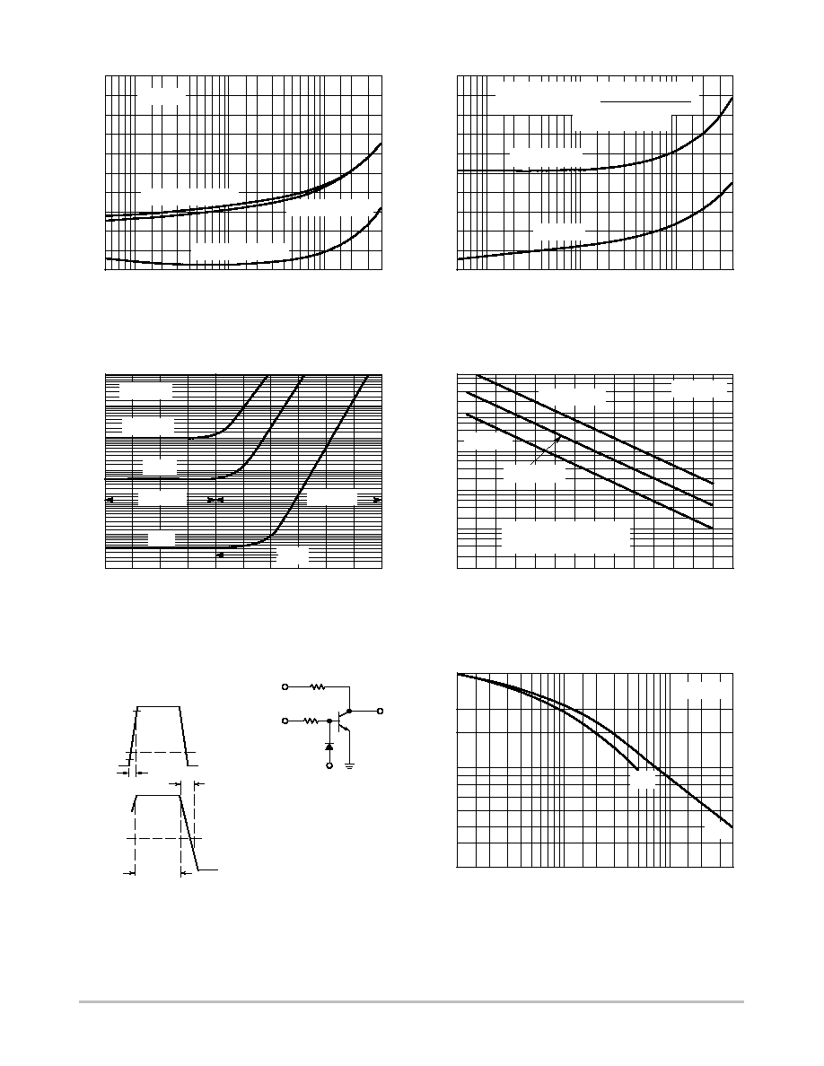
V CE
, COLLECT
OR-EMITTER VOL
T
AGE (VOL
TS)
Figure 1. DC Current Gain
IC, COLLECTOR CURRENT (AMP)
10
0.1
0.004
7.0
5.0
1.0
0.7
0.5
0.3
0.007 0.01
0.02
0.03
0.05
0.1
0.2
0.3
0.5
1.0
4.0
VCE = 2.0 V
VCE = 10 V
Figure 2. Collector Saturation Region
IB, BASE CURRENT (mA)
2.0
0
0.05
1.6
1.2
0.8
0.4
0.07 0.1
0.2
0.3
0.5 0.7 1.0
2.0
3.0
10
500
IC = 10 mA
2.0
3.0
TJ = 150
∞
C
-55
∞
C
25
∞
C
3.0
2.0
0.2
h FE
, DC CURRENT
GAIN (NORMALIZED)
5.0 7.0
20
30
50 70 100
200 300
100 mA
1.0 A
3.0 A
TJ = 25
∞
C
2N5191 2N5192
http://onsemi.com
3
R BE
, EXTERNAL
BASE-EMITTER RESIST
ANCE (OHMS)
2.0
0.005
IC, COLLECTOR CURRENT (AMP)
0.01 0.02 0.03 0.05
0.2 0.3
1.0
2.0
4.0
1.6
1.2
0.8
0.4
0
TJ = 25
∞
C
VBE(sat) @ IC/IB = 10
VCE(sat) @ IC/IB = 10
Figure 3. "On" Voltages
0.1
0.5
3.0
VBE @ VCE = 2.0 V
+2.5
Figure 4. Temperature Coefficients
IC, COLLECTOR CURRENT (AMP)
TJ = -65
∞
C to +150
∞
C
V,
TEMPERA
TURE COEFFICIENTS (mV/
C)
∞
+2.0
+1.5
+0.5
0
-0.5
-1.0
-1.5
-2.0
-2.5
V for VBE
*
V for VCE(sat)
*APPLIES FOR IC/IB
hFE @ VCE + 2.0 V
2
+1.0
0.005 0.01 0.02 0.03 0.05
0.2 0.3
1.0 2.0
4.0
0.1
0.5
3.0
103
-0.4
Figure 5. Collector Cut≠Off Region
VBE, BASE-EMITTER VOLTAGE (VOLTS)
102
101
100
10-1
10-2
10-3
-0.3 -0.2 -0.1
0
+0.1 +0.2 +0.3 +0.4 +0.5 +0.6
VCE = 30 V
TJ = 150
∞
C
100
∞
C
25
∞
C
REVERSE
FORWARD
ICES
107
20
Figure 6. Effects of Base≠Emitter Resistance
TJ, JUNCTION TEMPERATURE (
∞
C)
40
60
80
100
120
140
160
106
105
104
103
102
VCE = 30 V
IC = 10 x ICES
IC = 2 x ICES
IC
ICES
(TYPICAL ICES VALUES
OBTAINED FROM FIGURE 5)
Figure 7. Switching Time Equivalent Test Circuit
APPROX
+11 V
TURN-ON PULSE
Vin
t1
VEB(off)
TURN-OFF PULSE
Vin
t3
t2
APPROX
+11 V
VCC
SCOPE
RB
Cjd << Ceb
-4.0 V
t1
7.0 ns
100 < t2 < 500
µ
s
t3 < 15 ns
DUTY CYCLE
2.0%
APPROX -9.0 V
Vin
RC
0
RB and RC varied
to obtain desired
current levels
300
0.1
VR, REVERSE VOLTAGE (VOLTS)
0.2 0.3 0.5
1.0
3.0 5.0
20
40
200
100
70
50
30
TJ = +25
∞
C
CAP
ACIT
ANCE (pF)
Figure 8. Capacitance
2.0
10
30
Ceb
Ccb

2N5191 2N5192
http://onsemi.com
4
2.0
0.05
Figure 9. Turn≠On Time
IC, COLLECTOR CURRENT (AMP)
1.0
0.7
0.5
0.3
0.2
0.1
0.02
0.07 0.1
0.2
0.3
1.0
2.0
4.0
tr @ VCC = 30 V
IC/IB = 10
TJ = 25
∞
C
0.03
0.5
0.05
0.07
0.7
3.0
tr @ VCC = 10 V
td @ VEB(off) = 2.0 V
2.0
0.05
Figure 10. Turn≠Off Time
IC, COLLECTOR CURRENT (AMP)
1.0
0.7
0.5
0.3
0.2
0.1
0.02
0.07 0.1
0.2
0.3
1.0
2.0
4.0
tf @ VCC = 30 V
IB1 = IB2
IC/IB = 10
ts
= ts - 1/8 tf
TJ = 25
∞
C
0.03
t, TIME
(s)
µ
0.5
0.05
0.07
0.7
3.0
tf @ VCC = 10 V
ts
10
1.0
Figure 11. Rating and Thermal Data
Active≠Region Safe Operating Area
VCE, COLLECTOR-EMITTER VOLTAGE (VOLTS)
5.0
2.0
1.0
0.5
0.1
2.0
5.0
10
20
50
100
SECONDARY BREAKDOWN LIMIT
THERMAL LIMIT AT TC = 25
∞
C
BONDING WIRE LIMIT
0.2
I C
, COLLECT
OR CURRENT
(AMP)
CURVES APPLY BELOW RATED VCEO
TJ = 150
∞
C
dc
1.0 ms
100
µ
s
2N5191
2N5192
5.0 ms
There are two limitations on the power handling ability of
a transistor; average junction temperature and second
breakdown. Safe operating area curves indicate IC ≠ VCE
limits of the transistor that must be observed for reliable
operation; i.e., the transistor must not be subjected to greater
dissipation than the curves indicate.
The data of Figure 11 is based on TJ(pk) = 150_C; TC is
variable depending on conditions. Second breakdown pulse
limits are valid for duty cycles to 10% provided TJ(pk)
v 150_C. At high case temperatures, thermal limitations
will reduce the power that can be handled to values less than
the limitations imposed by second breakdown.
Figure 12. Thermal Response
t, TIME OR PULSE WIDTH (ms)
1.0
0.01
0.01
0.7
0.5
0.3
0.2
0.1
0.07
0.05
0.03
0.02
0.02 0.03
r(t)
, EFFECTIVE
TRANSIENT
THERMAL
RESIST
ANCE (NORMALIZED)
0.05
0.1
0.2
0.3 0.5 1.0
2.0
3.0 5.0 10
20
50
100
200
1000
500
JC(max) = 3.12
∞
C/W 2N5190-92
JC(max) = 2.08
∞
C/W MJE5190-92
D = 0.5
0.2
0.05
0.02
0.01
SINGLE PULSE
0.1

2N5191 2N5192
http://onsemi.com
5
DESIGN NOTE: USE OF TRANSIENT THERMAL RESISTANCE DATA
tP
PP
PP
t1
1/f
DUTY CYCLE, D = t1 f -
t1
tP
PEAK PULSE POWER = PP
Figure A
A train of periodical power pulses can be represented by
the model shown in Figure A. Using the model and the
device thermal response, the normalized effective transient
thermal resistance of Figure 12 was calculated for various
duty cycles.
To find
JC(t), multiply the value obtained from Figure 12
by the steady state value
JC.
Example:
The 2N5190 is dissipating 50 watts under the following
conditions: t1 = 0.1 ms, tp = 0.5 ms. (D = 0.2).
Using Figure 12, at a pulse width of 0.1 ms and D = 0.2,
the reading of r(t1, D) is 0.27.
The peak rise in function temperature is therefore:
T = r(t) x PP x
JC = 0.27 x 50 x 3.12 = 42.2
_
C