Plastic Darlington
Complementary Silicon Power
Transistors
. . . designed for general≠purpose amplifier and low≠speed
switching applications.
∑
High DC Current Gain --
hFE = 2000 (Typ) @ IC = 2.0 Adc
∑
Collector≠Emitter Sustaining Voltage -- @ 100 mAdc
VCEO(sus) = 60 Vdc (Min) -- 2N6035, 2N6038 = 80 Vdc
(Min) -- 2N6036, 2N6039
∑
Forward Biased Second Breakdown Current Capability
IS/b = 1.5 Adc @ 25 Vdc
∑
Monolithic Construction with Built≠In Base≠Emitter Resistors to
Limit
E
Leakage Multiplication
∑
Space≠Saving High Performance≠to≠Cost Ratio TO≠225AA Plastic
Package
ŒŒŒŒŒŒŒŒŒŒŒŒŒŒŒŒŒŒŒŒŒŒŒ
ŒŒŒŒŒŒŒŒŒŒŒŒŒŒŒŒŒŒŒŒŒŒŒ
MAXIMUM RATINGS (1)
ŒŒŒŒŒŒŒŒŒŒŒ
ŒŒŒŒŒŒŒŒŒŒŒ
Rating
ŒŒŒŒŒ
ŒŒŒŒŒ
Symbol
ŒŒŒŒ
ŒŒŒŒ
2N6035
2N6038
ŒŒŒŒ
ŒŒŒŒ
2N6036
2N6039
ŒŒŒ
ŒŒŒ
Unit
ŒŒŒŒŒŒŒŒŒŒŒ
ŒŒŒŒŒŒŒŒŒŒŒ
Collector≠Emitter Voltage
ŒŒŒŒŒ
ŒŒŒŒŒ
VCEO
ŒŒŒŒ
ŒŒŒŒ
60
ŒŒŒŒ
ŒŒŒŒ
80
ŒŒŒ
ŒŒŒ
Vdc
ŒŒŒŒŒŒŒŒŒŒŒ
ŒŒŒŒŒŒŒŒŒŒŒ
Collector≠Base Voltage
ŒŒŒŒŒ
ŒŒŒŒŒ
VCB
ŒŒŒŒ
ŒŒŒŒ
60
ŒŒŒŒ
ŒŒŒŒ
80
ŒŒŒ
ŒŒŒ
Vdc
ŒŒŒŒŒŒŒŒŒŒŒ
ŒŒŒŒŒŒŒŒŒŒŒ
Emitter≠Base Voltage
ŒŒŒŒŒ
ŒŒŒŒŒ
VEB
ŒŒŒŒŒŒŒ
ŒŒŒŒŒŒŒ
5.0
ŒŒŒ
ŒŒŒ
Vdc
ŒŒŒŒŒŒŒŒŒŒŒ
ŒŒŒŒŒŒŒŒŒŒŒ
Collector Current -- Continuous
Peak
ŒŒŒŒŒ
ŒŒŒŒŒ
IC
ŒŒŒŒŒŒŒ
ŒŒŒŒŒŒŒ
4.0
8.0
ŒŒŒ
ŒŒŒ
Adc
ŒŒŒŒŒŒŒŒŒŒŒ
ŒŒŒŒŒŒŒŒŒŒŒ
Base Current
ŒŒŒŒŒ
ŒŒŒŒŒ
IB
ŒŒŒŒŒŒŒ
ŒŒŒŒŒŒŒ
100
ŒŒŒ
ŒŒŒ
mAdc
ŒŒŒŒŒŒŒŒŒŒŒ
ŒŒŒŒŒŒŒŒŒŒŒ
Total Power Dissipation @ TC = 25
_
C
Derate above 25
_
C
ŒŒŒŒŒ
ŒŒŒŒŒ
PD
ŒŒŒŒŒŒŒ
ŒŒŒŒŒŒŒ
40
0.32
ŒŒŒ
ŒŒŒ
Watts
W/
_
C
ŒŒŒŒŒŒŒŒŒŒŒ
Œ
ŒŒŒŒŒŒŒŒŒ
Œ
ŒŒŒŒŒŒŒŒŒŒŒ
Total Power Dissipation @ TA = 25
_
C
Derate above 25
_
C
ŒŒŒŒŒ
Œ
ŒŒŒ
Œ
ŒŒŒŒŒ
PD
ŒŒŒŒŒŒŒ
Œ
ŒŒŒŒŒ
Œ
ŒŒŒŒŒŒŒ
1.5
0.012
ŒŒŒ
Œ
Œ
Œ
ŒŒŒ
Watts
ŒŒŒŒŒŒŒŒŒŒŒ
ŒŒŒŒŒŒŒŒŒŒŒ
Operating and Storage Junction
Temperature Range
ŒŒŒŒŒ
ŒŒŒŒŒ
TJ, Tstg
ŒŒŒŒŒŒŒ
ŒŒŒŒŒŒŒ
≠65 to +150
ŒŒŒ
ŒŒŒ
_
C
ŒŒŒŒŒŒŒŒŒŒŒŒŒŒŒŒŒŒŒŒŒŒŒ
ŒŒŒŒŒŒŒŒŒŒŒŒŒŒŒŒŒŒŒŒŒŒŒ
THERMAL CHARACTERISTICS
ŒŒŒŒŒŒŒŒŒŒŒŒ
ŒŒŒŒŒŒŒŒŒŒŒŒ
Characteristic
ŒŒŒŒŒ
ŒŒŒŒŒ
Symbol
ŒŒŒŒŒŒ
ŒŒŒŒŒŒ
Max
ŒŒŒ
ŒŒŒ
Unit
ŒŒŒŒŒŒŒŒŒŒŒŒ
ŒŒŒŒŒŒŒŒŒŒŒŒ
Thermal Resistance, Junction to Case
ŒŒŒŒŒ
ŒŒŒŒŒ
JC
ŒŒŒŒŒŒ
ŒŒŒŒŒŒ
3.12
ŒŒŒ
ŒŒŒ
_
C/W
ŒŒŒŒŒŒŒŒŒŒŒŒ
ŒŒŒŒŒŒŒŒŒŒŒŒ
Thermal Resistance, Junction to Ambient
ŒŒŒŒŒ
ŒŒŒŒŒ
JA
ŒŒŒŒŒŒ
ŒŒŒŒŒŒ
83.3
ŒŒŒ
ŒŒŒ
_
C/W
(1) Indicates JEDEC Registered Data.
Preferred devices are ON Semiconductor recommended choices for future use and best overall value.
ON Semiconductor
)
©
Semiconductor Components Industries, LLC, 2002
April, 2002 ≠ Rev. 10
1
Publication Order Number:
2N6035/D
2N6035
2N6036
2N6038
2N6039
*ON Semiconductor Preferred Device
DARLINGTON
4≠AMPERE
COMPLEMENTARY
SILICON
POWER TRANSISTORS
60, 80 VOLTS
40 WATTS
*
*
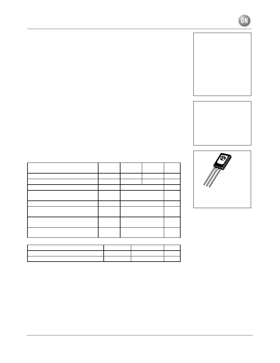
CASE 77≠09
TO≠225AA TYPE
PNP
NPN
3
2 1
STYLE 1:
PIN 1. EMITTER
2. COLLECTOR
3. BASE

2N6035 2N6036 2N6038 2N6039
http://onsemi.com
3
ŒŒŒŒŒŒŒŒŒŒŒŒŒŒŒŒŒŒŒŒŒŒŒŒŒŒŒŒŒŒŒŒŒ
ŒŒŒŒŒŒŒŒŒŒŒŒŒŒŒŒŒŒŒŒŒŒŒŒŒŒŒŒŒŒŒŒŒ
ELECTRICAL CHARACTERISTICS
(TC = 25
_
C unless otherwise noted)
ŒŒŒŒŒŒŒŒŒŒŒŒŒŒŒŒŒŒŒŒŒŒ
Œ
ŒŒŒŒŒŒŒŒŒŒŒŒŒŒŒŒŒŒŒŒ
Œ
ŒŒŒŒŒŒŒŒŒŒŒŒŒŒŒŒŒŒŒŒŒŒ
Characteristic
ŒŒŒŒŒ
Œ
ŒŒŒ
Œ
ŒŒŒŒŒ
Symbol
ŒŒŒ
Œ
Œ
Œ
ŒŒŒ
Min
ŒŒŒŒ
Œ
ŒŒ
Œ
ŒŒŒŒ
Max
ŒŒŒ
Œ
Œ
Œ
ŒŒŒ
Unit
ŒŒŒŒŒŒŒŒŒŒŒŒŒŒŒŒŒŒŒŒŒŒŒŒŒŒŒŒŒŒŒŒŒ
ŒŒŒŒŒŒŒŒŒŒŒŒŒŒŒŒŒŒŒŒŒŒŒŒŒŒŒŒŒŒŒŒŒ
OFF CHARACTERISTICS
ŒŒŒŒŒŒŒŒŒŒŒŒŒŒŒŒŒŒŒŒŒŒ
Œ
ŒŒŒŒŒŒŒŒŒŒŒŒŒŒŒŒŒŒŒŒ
Œ
ŒŒŒŒŒŒŒŒŒŒŒŒŒŒŒŒŒŒŒŒŒŒ
Collector≠Emitter Sustaining Voltage
(IC = 100 mAdc, IB = 0)
2N6035, 2N6038
2N6036, 2N6039
ŒŒŒŒŒ
Œ
ŒŒŒ
Œ
ŒŒŒŒŒ
VCEO(sus)
ŒŒŒ
Œ
Œ
Œ
ŒŒŒ
60
80
ŒŒŒŒ
Œ
ŒŒ
Œ
ŒŒŒŒ
--
--
ŒŒŒ
Œ
Œ
Œ
ŒŒŒ
Vdc
ŒŒŒŒŒŒŒŒŒŒŒŒŒŒŒŒŒŒŒŒŒŒ
Œ
ŒŒŒŒŒŒŒŒŒŒŒŒŒŒŒŒŒŒŒŒ
Œ
Œ
ŒŒŒŒŒŒŒŒŒŒŒŒŒŒŒŒŒŒŒŒ
Œ
ŒŒŒŒŒŒŒŒŒŒŒŒŒŒŒŒŒŒŒŒŒŒ
Collector≠Cutoff Current
(VCE = 60 Vdc, IB = 0)
2N6035, 2N6038
(VCE = 80 Vdc, IB = 0)
2N6036, 2N6039
ŒŒŒŒŒ
Œ
ŒŒŒ
Œ
Œ
ŒŒŒ
Œ
ŒŒŒŒŒ
ICEO
ŒŒŒ
Œ
Œ
Œ
Œ
Œ
Œ
ŒŒŒ
--
--
ŒŒŒŒ
Œ
ŒŒ
Œ
Œ
ŒŒ
Œ
ŒŒŒŒ
100
100
ŒŒŒ
Œ
Œ
Œ
Œ
Œ
Œ
ŒŒŒ
µ
A
ŒŒŒŒŒŒŒŒŒŒŒŒŒŒŒŒŒŒŒŒŒŒ
Œ
ŒŒŒŒŒŒŒŒŒŒŒŒŒŒŒŒŒŒŒŒ
Œ
Œ
ŒŒŒŒŒŒŒŒŒŒŒŒŒŒŒŒŒŒŒŒ
Œ
Œ
ŒŒŒŒŒŒŒŒŒŒŒŒŒŒŒŒŒŒŒŒ
Œ
ŒŒŒŒŒŒŒŒŒŒŒŒŒŒŒŒŒŒŒŒŒŒ
Collector≠Cutoff Current
(VCE = 60 Vdc, VBE(off) = 1.5 Vdc)
2N6035, 2N6038
(VCE = 80 Vdc, VBE(off) = 1.5 Vdc)
2N6036, 2N6039
(VCE = 60 Vdc, VBE(off) = 1.5 Vdc, TC = 125
_
C)
2N6035, 2N6038
(VCE = 80 Vdc, VBE(off) = 1.5 Vdc, TC = 125
_
C)
2N6036, 2N6039
ŒŒŒŒŒ
Œ
ŒŒŒ
Œ
Œ
ŒŒŒ
Œ
Œ
ŒŒŒ
Œ
ŒŒŒŒŒ
ICEX
ŒŒŒ
Œ
Œ
Œ
Œ
Œ
Œ
Œ
Œ
Œ
ŒŒŒ
--
--
--
--
ŒŒŒŒ
Œ
ŒŒ
Œ
Œ
ŒŒ
Œ
Œ
ŒŒ
Œ
ŒŒŒŒ
100
100
500
500
ŒŒŒ
Œ
Œ
Œ
Œ
Œ
Œ
Œ
Œ
Œ
ŒŒŒ
µ
A
ŒŒŒŒŒŒŒŒŒŒŒŒŒŒŒŒŒŒŒŒŒŒ
Œ
ŒŒŒŒŒŒŒŒŒŒŒŒŒŒŒŒŒŒŒŒ
Œ
ŒŒŒŒŒŒŒŒŒŒŒŒŒŒŒŒŒŒŒŒŒŒ
Collector≠Cutoff Current
(VCB = 60 Vdc, IE = 0)
2N6035, 2N6038
(VCB = 80 Vdc, IE = 0)
2N6036, 2N6039
ŒŒŒŒŒ
Œ
ŒŒŒ
Œ
ŒŒŒŒŒ
ICBO
ŒŒŒ
Œ
Œ
Œ
ŒŒŒ
--
--
ŒŒŒŒ
Œ
ŒŒ
Œ
ŒŒŒŒ
0.5
0.5
ŒŒŒ
Œ
Œ
Œ
ŒŒŒ
mAdc
ŒŒŒŒŒŒŒŒŒŒŒŒŒŒŒŒŒŒŒŒŒŒ
ŒŒŒŒŒŒŒŒŒŒŒŒŒŒŒŒŒŒŒŒŒŒ
Emitter≠Cutoff Current (VBE = 5.0 Vdc, IC = 0)
ŒŒŒŒŒ
ŒŒŒŒŒ
IEBO
ŒŒŒ
ŒŒŒ
--
ŒŒŒŒ
ŒŒŒŒ
2.0
ŒŒŒ
ŒŒŒ
mAdc
ŒŒŒŒŒŒŒŒŒŒŒŒŒŒŒŒŒŒŒŒŒŒŒŒŒŒŒŒŒŒŒŒŒ
ŒŒŒŒŒŒŒŒŒŒŒŒŒŒŒŒŒŒŒŒŒŒŒŒŒŒŒŒŒŒŒŒŒ
ON CHARACTERISTICS
ŒŒŒŒŒŒŒŒŒŒŒŒŒŒŒŒŒŒŒŒŒŒ
Œ
ŒŒŒŒŒŒŒŒŒŒŒŒŒŒŒŒŒŒŒŒ
Œ
Œ
ŒŒŒŒŒŒŒŒŒŒŒŒŒŒŒŒŒŒŒŒ
Œ
ŒŒŒŒŒŒŒŒŒŒŒŒŒŒŒŒŒŒŒŒŒŒ
DC Current Gain
(IC = 0.5 Adc, VCE = 3.0 Vdc)
(IC = 2.0 Adc, VCE = 3.0 Vdc)
(IC = 4.0 Adc, VCE = 3.0 Vdc)
ŒŒŒŒŒ
Œ
ŒŒŒ
Œ
Œ
ŒŒŒ
Œ
ŒŒŒŒŒ
hFE
ŒŒŒ
Œ
Œ
Œ
Œ
Œ
Œ
ŒŒŒ
500
750
100
ŒŒŒŒ
Œ
ŒŒ
Œ
Œ
ŒŒ
Œ
ŒŒŒŒ
--
15,000
--
ŒŒŒ
Œ
Œ
Œ
Œ
Œ
Œ
ŒŒŒ
--
ŒŒŒŒŒŒŒŒŒŒŒŒŒŒŒŒŒŒŒŒŒŒ
Œ
ŒŒŒŒŒŒŒŒŒŒŒŒŒŒŒŒŒŒŒŒ
Œ
Œ
ŒŒŒŒŒŒŒŒŒŒŒŒŒŒŒŒŒŒŒŒ
Œ
ŒŒŒŒŒŒŒŒŒŒŒŒŒŒŒŒŒŒŒŒŒŒ
Collector≠Emitter Saturation Voltage
(IC = 2.0 Adc, IB = 8.0 mAdc)
(IC = 4.0 Adc, IB = 40 mAdc)
ŒŒŒŒŒ
Œ
ŒŒŒ
Œ
Œ
ŒŒŒ
Œ
ŒŒŒŒŒ
VCE(sat)
ŒŒŒ
Œ
Œ
Œ
Œ
Œ
Œ
ŒŒŒ
--
--
ŒŒŒŒ
Œ
ŒŒ
Œ
Œ
ŒŒ
Œ
ŒŒŒŒ
2.0
3.0
ŒŒŒ
Œ
Œ
Œ
Œ
Œ
Œ
ŒŒŒ
Vdc
ŒŒŒŒŒŒŒŒŒŒŒŒŒŒŒŒŒŒŒŒŒŒ
ŒŒŒŒŒŒŒŒŒŒŒŒŒŒŒŒŒŒŒŒŒŒ
Base≠Emitter Saturation Voltage (IC = 4.0 Adc, IB = 40 mAdc)
ŒŒŒŒŒ
ŒŒŒŒŒ
VBE(sat)
ŒŒŒ
ŒŒŒ
--
ŒŒŒŒ
ŒŒŒŒ
4.0
ŒŒŒ
ŒŒŒ
Vdc
ŒŒŒŒŒŒŒŒŒŒŒŒŒŒŒŒŒŒŒŒŒŒ
ŒŒŒŒŒŒŒŒŒŒŒŒŒŒŒŒŒŒŒŒŒŒ
Base≠Emitter On Voltage (IC = 2.0 Adc, VCE = 3.0 Vdc)
ŒŒŒŒŒ
ŒŒŒŒŒ
VBE(on)
ŒŒŒ
ŒŒŒ
--
ŒŒŒŒ
ŒŒŒŒ
2.8
ŒŒŒ
ŒŒŒ
Vdc
ŒŒŒŒŒŒŒŒŒŒŒŒŒŒŒŒŒŒŒŒŒŒŒŒŒŒŒŒŒŒŒŒŒ
ŒŒŒŒŒŒŒŒŒŒŒŒŒŒŒŒŒŒŒŒŒŒŒŒŒŒŒŒŒŒŒŒŒ
DYNAMIC CHARACTERISTICS
ŒŒŒŒŒŒŒŒŒŒŒŒŒŒŒŒŒŒŒŒŒŒ
ŒŒŒŒŒŒŒŒŒŒŒŒŒŒŒŒŒŒŒŒŒŒ
Small≠Signal Current≠Gain (IC = 0.75 Adc, VCE = 10 Vdc, f = 1.0 MHz)
ŒŒŒŒŒ
ŒŒŒŒŒ
|hfe|
ŒŒŒ
ŒŒŒ
25
ŒŒŒŒ
ŒŒŒŒ
--
ŒŒŒ
ŒŒŒ
--
ŒŒŒŒŒŒŒŒŒŒŒŒŒŒŒŒŒŒŒŒŒŒ
Œ
ŒŒŒŒŒŒŒŒŒŒŒŒŒŒŒŒŒŒŒŒ
Œ
Œ
ŒŒŒŒŒŒŒŒŒŒŒŒŒŒŒŒŒŒŒŒ
Œ
ŒŒŒŒŒŒŒŒŒŒŒŒŒŒŒŒŒŒŒŒŒŒ
Output Capacitance
(VCB = 10 Vdc, IE = 0, f = 0.1 MHz)
2N6035, 2N6036
2N6038, 2N6039
ŒŒŒŒŒ
Œ
ŒŒŒ
Œ
Œ
ŒŒŒ
Œ
ŒŒŒŒŒ
Cob
ŒŒŒ
Œ
Œ
Œ
Œ
Œ
Œ
ŒŒŒ
--
--
ŒŒŒŒ
Œ
ŒŒ
Œ
Œ
ŒŒ
Œ
ŒŒŒŒ
200
100
ŒŒŒ
Œ
Œ
Œ
Œ
Œ
Œ
ŒŒŒ
pF
*Indicates JEDEC Registered Data.
Figure 2. Switching Times Test Circuit
4.0
0.04
Figure 3. Switching Times
IC, COLLECTOR CURRENT (AMP)
t, TIME
(s)
µ
2.0
1.0
0.6
0.2
0.06
0.1
0.2
0.4 0.6
1.0
2.0
4.0
0.4
0.8
PNP
NPN
tf
tr
ts
td @ VBE(off) = 0
V2
approx
+8.0 V
V1
approx
-12 V
tr, tf
10 ns
DUTY CYCLE = 1.0%
25
µ
s
0
RB
51
D1
+4.0 V
VCC
-30 V
RC
TUT
8.0 k
60
SCOPE
for td and tr, D1 is disconnected
and V2 = 0, RB and RC are varied
to obtain desired test currents.
For NPN test circuit, reverse diode,
polarities and input pulses.
RB & RC VARIED TO OBTAIN DESIRED CURRENT LEVELS
D1 MUST BE FAST RECOVERY TYPE, eg:
1N5825 USED ABOVE IB
100 mA
MSD6100 USED BELOW IB
100 mA
VCC = 30 V
IC/IB = 250
IB1 = IB2
TJ = 25
∞
C
2N6035 2N6036 2N6038 2N6039
http://onsemi.com
5
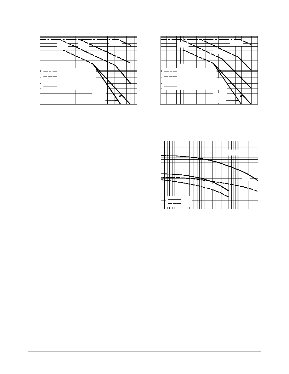
ACTIVE≠REGION SAFE≠OPERATING AREA
1.0
5.0
Figure 5. 2N6035, 2N6036
VCE, COLLECTOR-EMITTER VOLTAGE (VOLTS)
7.0
5.0
3.0
2.0
0.1
7.0
10
30
50
100
BONDING WIRE LIMITED
THERMALLY LIMITED
70
1.0
I C
, COLLECT
OR CURRENT
(AMP)
TJ = 150
∞
C
dc
1.0 ms
100
µ
s
Figure 6. 2N6038, 2N6039
0.7
0.5
0.2
20
2N6036
2N6035
0.3
1.0
5.0
VCE, COLLECTOR-EMITTER VOLTAGE (VOLTS)
7.0
5.0
3.0
2.0
0.1
7.0
10
30
50
100
70
1.0
I C
, COLLECT
OR CURRENT
(AMP)
0.7
0.5
0.2
20
2N6039
2N6038
0.3
5.0 ms
@ TC = 25
∞
C (SINGLE PULSE)
SECOND BREAKDOWN LIMITED
100
µ
s
1.0 ms
5.0 ms
dc
BONDING WIRE LIMITED
THERMALLY LIMITED
TJ = 150
∞
C
@ TC = 25
∞
C (SINGLE PULSE)
SECOND BREAKDOWN LIMITED
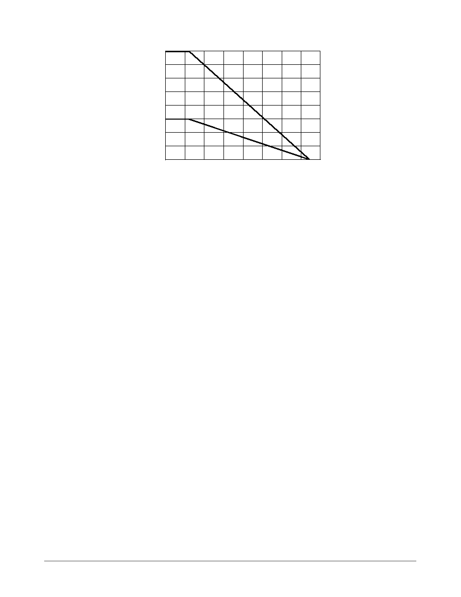
There are two limitations on the power handling ability of
a transistor: average junction temperature and second
breakdown. Safe operating area curves indicate IC ≠ VCE
limits of the transistor that must be observed for reliable
operation; i.e., the transistor must not be subjected to greater
dissipation than the curves indicate.
The data of Figures 5 and 6 is based on TJ(pk) = 150_C;
TC is variable depending on conditions. Second breakdown
pulse limits are valid for duty cycles to 10% provided TJ(pk)
< 150
_C. TJ(pk) may be calculated from the data in Figure 4.
At high case temperatures, thermal limitations will reduce
the power that can be handled to values less than the
limitations imposed by second breakdown.
200
0.04
VR, REVERSE VOLTAGE (VOLTS)
10
0.4 0.6 1.0
2.0
40
4.0
0.06 0.1
0.2
C, CAP
ACIT
ANCE (pF)
100
50
30
TC = 25
∞
C
Cib
70
Cob
PNP
NPN
Figure 7. Capacitance
20
6.0 10
20