 | ÐлекÑÑоннÑй компоненÑ: 2N6043 | СкаÑаÑÑ:  PDF PDF  ZIP ZIP |
Äîêóìåíòàöèÿ è îïèñàíèÿ www.docs.chipfind.ru
Plastic Medium-Power
Complementary Silicon
Transistors
. . . designed for generalpurpose amplifier and lowspeed
switching applications.
·
High DC Current Gain
hFE = 2500 (Typ) @ IC = 4.0 Adc
·
CollectorEmitter Sustaining Voltage @ 100 mAdc
VCEO(sus) = 60 Vdc (Min) 2N6040, 2N6043
= 100 Vdc (Min) 2N6042, 2N6045
·
Low CollectorEmitter Saturation Voltage
VCE(sat) = 2.0 Vdc (Max) @ IC = 4.0 Adc 2N6043,44
= 2.0 Vdc (Max) @ IC = 3.0 Adc 2N6042, 2N6045
·
Monolithic Construction with BuiltIn BaseEmitter Shunt Resistors
ÎÎÎÎÎÎÎÎÎÎÎÎÎÎÎÎÎÎÎÎÎÎÎ
ÎÎÎÎÎÎÎÎÎÎÎÎÎÎÎÎÎÎÎÎÎÎÎ
MAXIMUM RATINGS (1)
ÎÎÎÎÎÎÎÎÎÎÎÎ
Î
ÎÎÎÎÎÎÎÎÎÎ
Î
ÎÎÎÎÎÎÎÎÎÎÎÎ
Rating
ÎÎÎÎ
Î
ÎÎ
Î
ÎÎÎÎ
Symbol
ÎÎÎÎ
Î
ÎÎ
Î
ÎÎÎÎ
2N6040
2N6043
ÎÎÎÎ
Î
ÎÎ
Î
ÎÎÎÎ
2N6042
2N6045
ÎÎÎ
Î
Î
Î
ÎÎÎ
Unit
ÎÎÎÎÎÎÎÎÎÎÎÎ
ÎÎÎÎÎÎÎÎÎÎÎÎ
CollectorEmitter Voltage
ÎÎÎÎ
ÎÎÎÎ
VCEO
ÎÎÎÎ
ÎÎÎÎ
60
ÎÎÎÎ
ÎÎÎÎ
100
ÎÎÎ
ÎÎÎ
Vdc
ÎÎÎÎÎÎÎÎÎÎÎÎ
CollectorBase Voltage
ÎÎÎÎ
VCB
ÎÎÎÎ
60
ÎÎÎÎ
100
ÎÎÎ
Vdc
ÎÎÎÎÎÎÎÎÎÎÎÎ
ÎÎÎÎÎÎÎÎÎÎÎÎ
EmitterBase Voltage
ÎÎÎÎ
ÎÎÎÎ
VEB
ÎÎÎÎÎÎÎ
ÎÎÎÎÎÎÎ
5.0
ÎÎÎ
ÎÎÎ
Vdc
ÎÎÎÎÎÎÎÎÎÎÎÎ
Î
ÎÎÎÎÎÎÎÎÎÎ
Î
ÎÎÎÎÎÎÎÎÎÎÎÎ
Collector Current Continuous
Peak
ÎÎÎÎ
Î
ÎÎ
Î
ÎÎÎÎ
IC
ÎÎÎÎÎÎÎ
Î
ÎÎÎÎÎ
Î
ÎÎÎÎÎÎÎ
8.0
16
ÎÎÎ
Î
Î
Î
ÎÎÎ
Adc
ÎÎÎÎÎÎÎÎÎÎÎÎ
ÎÎÎÎÎÎÎÎÎÎÎÎ
Base Current
ÎÎÎÎ
ÎÎÎÎ
IB
ÎÎÎÎÎÎÎ
ÎÎÎÎÎÎÎ
120
ÎÎÎ
ÎÎÎ
mAdc
ÎÎÎÎÎÎÎÎÎÎÎÎ
ÎÎÎÎÎÎÎÎÎÎÎÎ
Total Power Dissipation @ TC = 25
_
C
Derate above 25
_
C
ÎÎÎÎ
ÎÎÎÎ
PD
ÎÎÎÎÎÎÎ
ÎÎÎÎÎÎÎ
75
0.60
ÎÎÎ
ÎÎÎ
Watts
W/
_
C
ÎÎÎÎÎÎÎÎÎÎÎÎ
ÎÎÎÎÎÎÎÎÎÎÎÎ
Operating and Storage Junction,
Temperature Range
ÎÎÎÎ
ÎÎÎÎ
TJ, Tstg
ÎÎÎÎÎÎÎ
ÎÎÎÎÎÎÎ
65 to +150
ÎÎÎ
ÎÎÎ
_
C
ÎÎÎÎÎÎÎÎÎÎÎÎÎÎÎÎÎÎÎÎÎÎÎ
ÎÎÎÎÎÎÎÎÎÎÎÎÎÎÎÎÎÎÎÎÎÎÎ
THERMAL CHARACTERISTICS
ÎÎÎÎÎÎÎÎÎÎÎÎ
ÎÎÎÎÎÎÎÎÎÎÎÎ
Characteristic
ÎÎÎÎÎ
ÎÎÎÎÎ
Symbol
ÎÎÎÎÎÎ
ÎÎÎÎÎÎ
Max
ÎÎÎ
ÎÎÎ
Unit
ÎÎÎÎÎÎÎÎÎÎÎÎ
ÎÎÎÎÎÎÎÎÎÎÎÎ
Thermal Resistance, Junction to Case
ÎÎÎÎÎ
ÎÎÎÎÎ
JC
ÎÎÎÎÎÎ
ÎÎÎÎÎÎ
1.67
ÎÎÎ
ÎÎÎ
_
C/W
ÎÎÎÎÎÎÎÎÎÎÎÎ
ÎÎÎÎÎÎÎÎÎÎÎÎ
Thermal Resistance, Junction to Ambient
ÎÎÎÎÎ
ÎÎÎÎÎ
JA
ÎÎÎÎÎÎ
ÎÎÎÎÎÎ
57
ÎÎÎ
ÎÎÎ
_
C/W
(1) Indicates JEDEC Registered Data.
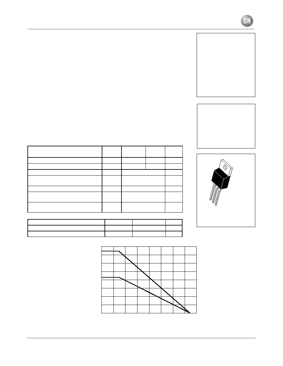
80
0
0
20
40
60
80
100
120
160
Figure 1. Power Derating
T, TEMPERATURE (
°
C)
P D
, POWER DISSIP
A
TION (W
A
TTS)
40
20
60
140
TC
4.0
0
2.0
1.0
3.0
TA
TA
TC
Preferred devices are ON Semiconductor recommended choices for future use and best overall value.
ON Semiconductor
)
©
Semiconductor Components Industries, LLC, 2002
April, 2002 Rev. 4
1
Publication Order Number:
2N6040/D
2N6040
2N6042
2N6043
2N6045
*ON Semiconductor Preferred Device
DARLINGTON
8 AMPERE
COMPLEMENTARY
SILICON
POWER TRANSISTORS
60100 VOLTS
75 WATTS
*
*
CASE 221A09
TO220AB
PNP
NPN
STYLE 1:
PIN 1. BASE
2. COLLECTOR
3. EMITTER
4. COLLECTOR
1
2
3
4
2N6040 2N6042 2N6043 2N6045
http://onsemi.com
2
ÎÎÎÎÎÎÎÎÎÎÎÎÎÎÎÎÎÎÎÎÎÎÎÎÎÎÎÎÎÎÎÎÎ
ÎÎÎÎÎÎÎÎÎÎÎÎÎÎÎÎÎÎÎÎÎÎÎÎÎÎÎÎÎÎÎÎÎ
*ELECTRICAL CHARACTERISTICS
(TC = 25
_
C unless otherwise noted)
ÎÎÎÎÎÎÎÎÎÎÎÎÎÎÎÎÎÎÎÎÎÎ
ÎÎÎÎÎÎÎÎÎÎÎÎÎÎÎÎÎÎÎÎÎÎ
Characteristic
ÎÎÎÎÎ
ÎÎÎÎÎ
Symbol
ÎÎÎ
ÎÎÎ
Min
ÎÎÎÎ
ÎÎÎÎ
Max
ÎÎÎ
ÎÎÎ
Unit
ÎÎÎÎÎÎÎÎÎÎÎÎÎÎÎÎÎÎÎÎÎÎÎÎÎÎÎÎÎÎÎÎÎ
ÎÎÎÎÎÎÎÎÎÎÎÎÎÎÎÎÎÎÎÎÎÎÎÎÎÎÎÎÎÎÎÎÎ
OFF CHARACTERISTICS
ÎÎÎÎÎÎÎÎÎÎÎÎÎÎÎÎÎÎÎÎÎÎ
Î
ÎÎÎÎÎÎÎÎÎÎÎÎÎÎÎÎÎÎÎÎ
Î
Î
ÎÎÎÎÎÎÎÎÎÎÎÎÎÎÎÎÎÎÎÎ
Î
ÎÎÎÎÎÎÎÎÎÎÎÎÎÎÎÎÎÎÎÎÎÎ
CollectorEmitter Sustaining Voltage
(IC = 100 mAdc, IB = 0)
2N6040, 2N6043
2N6042, 2N6045
ÎÎÎÎÎ
Î
ÎÎÎ
Î
Î
ÎÎÎ
Î
ÎÎÎÎÎ
VCEO(sus)
ÎÎÎ
Î
Î
Î
Î
Î
Î
ÎÎÎ
60
100
ÎÎÎÎ
Î
ÎÎ
Î
Î
ÎÎ
Î
ÎÎÎÎ
ÎÎÎ
Î
Î
Î
Î
Î
Î
ÎÎÎ
Vdc
ÎÎÎÎÎÎÎÎÎÎÎÎÎÎÎÎÎÎÎÎÎÎ
Î
ÎÎÎÎÎÎÎÎÎÎÎÎÎÎÎÎÎÎÎÎ
Î
ÎÎÎÎÎÎÎÎÎÎÎÎÎÎÎÎÎÎÎÎÎÎ
Collector Cutoff Current
(VCE = 60 Vdc, IB = 0)
2N6040, 2N6043
(VCE = 100 Vdc, IB = 0)
2N6042, 2N6045
ÎÎÎÎÎ
Î
ÎÎÎ
Î
ÎÎÎÎÎ
ICEO
ÎÎÎ
Î
Î
Î
ÎÎÎ
ÎÎÎÎ
Î
ÎÎ
Î
ÎÎÎÎ
20
20
ÎÎÎ
Î
Î
Î
ÎÎÎ
µ
A
ÎÎÎÎÎÎÎÎÎÎÎÎÎÎÎÎÎÎÎÎÎÎ
Î
ÎÎÎÎÎÎÎÎÎÎÎÎÎÎÎÎÎÎÎÎ
Î
Î
ÎÎÎÎÎÎÎÎÎÎÎÎÎÎÎÎÎÎÎÎ
Î
Î
ÎÎÎÎÎÎÎÎÎÎÎÎÎÎÎÎÎÎÎÎ
Î
Î
ÎÎÎÎÎÎÎÎÎÎÎÎÎÎÎÎÎÎÎÎ
Î
ÎÎÎÎÎÎÎÎÎÎÎÎÎÎÎÎÎÎÎÎÎÎ
Collector Cutoff Current
(VCE = 60 Vdc, VBE(off) = 1.5 Vdc)
2N6040, 2N6043
(VCE = 100 Vdc, VBE(off) = 1.5 Vdc)
2N6042, 2N6045
(VCE = 60 Vdc, VBE(off) = 1.5 Vdc, TC = 150
_
C)
2N6040, 2N6043
(VCE = 80 Vdc, VBE(off) = 1.5 Vdc, TC = 150
_
C)
2N6041, 2N6044
(VCE = 100 Vdc, VBE(off) = 1.5 Vdc, TC = 150
_
C)
2N6042, 2N6045
ÎÎÎÎÎ
Î
ÎÎÎ
Î
Î
ÎÎÎ
Î
Î
ÎÎÎ
Î
Î
ÎÎÎ
Î
ÎÎÎÎÎ
ICEX
ÎÎÎ
Î
Î
Î
Î
Î
Î
Î
Î
Î
Î
Î
Î
ÎÎÎ
ÎÎÎÎ
Î
ÎÎ
Î
Î
ÎÎ
Î
Î
ÎÎ
Î
Î
ÎÎ
Î
ÎÎÎÎ
20
20
200
200
200
ÎÎÎ
Î
Î
Î
Î
Î
Î
Î
Î
Î
Î
Î
Î
ÎÎÎ
µ
A
ÎÎÎÎÎÎÎÎÎÎÎÎÎÎÎÎÎÎÎÎÎÎ
Î
ÎÎÎÎÎÎÎÎÎÎÎÎÎÎÎÎÎÎÎÎ
Î
Î
ÎÎÎÎÎÎÎÎÎÎÎÎÎÎÎÎÎÎÎÎ
Î
ÎÎÎÎÎÎÎÎÎÎÎÎÎÎÎÎÎÎÎÎÎÎ
Collector Cutoff Current
(VCB = 60 Vdc, IE = 0)
2N6040, 2N6043
(VCB = 100 Vdc, IE = 0)
2N6042, 2N6045
ÎÎÎÎÎ
Î
ÎÎÎ
Î
Î
ÎÎÎ
Î
ÎÎÎÎÎ
ICBO
ÎÎÎ
Î
Î
Î
Î
Î
Î
ÎÎÎ
ÎÎÎÎ
Î
ÎÎ
Î
Î
ÎÎ
Î
ÎÎÎÎ
20
20
ÎÎÎ
Î
Î
Î
Î
Î
Î
ÎÎÎ
µ
A
ÎÎÎÎÎÎÎÎÎÎÎÎÎÎÎÎÎÎÎÎÎÎ
ÎÎÎÎÎÎÎÎÎÎÎÎÎÎÎÎÎÎÎÎÎÎ
Emitter Cutoff Current (VBE = 5.0 Vdc, IC = 0)
ÎÎÎÎÎ
ÎÎÎÎÎ
IEBO
ÎÎÎ
ÎÎÎ
ÎÎÎÎ
ÎÎÎÎ
2.0
ÎÎÎ
ÎÎÎ
mAdc
ÎÎÎÎÎÎÎÎÎÎÎÎÎÎÎÎÎÎÎÎÎÎÎÎÎÎÎÎÎÎÎÎÎ
ON CHARACTERISTICS
ÎÎÎÎÎÎÎÎÎÎÎÎÎÎÎÎÎÎÎÎÎÎ
Î
ÎÎÎÎÎÎÎÎÎÎÎÎÎÎÎÎÎÎÎÎ
Î
Î
ÎÎÎÎÎÎÎÎÎÎÎÎÎÎÎÎÎÎÎÎ
Î
ÎÎÎÎÎÎÎÎÎÎÎÎÎÎÎÎÎÎÎÎÎÎ
DC Current Gain
(IC = 4.0 Adc, VCE = 4.0 Vdc)
2N6040, 2N6043,
(IC = 3.0 Adc, VCE = 4.0 Vdc)
2N6042, 2N6045
(IC = 8.0 Adc, VCE = 4.0 Vdc)
All Types
ÎÎÎÎÎ
Î
ÎÎÎ
Î
Î
ÎÎÎ
Î
ÎÎÎÎÎ
hFE
ÎÎÎ
Î
Î
Î
Î
Î
Î
ÎÎÎ
1000
1000
100
ÎÎÎÎ
Î
ÎÎ
Î
Î
ÎÎ
Î
ÎÎÎÎ
20.000
20,000
ÎÎÎ
Î
Î
Î
Î
Î
Î
ÎÎÎ
ÎÎÎÎÎÎÎÎÎÎÎÎÎÎÎÎÎÎÎÎÎÎ
Î
ÎÎÎÎÎÎÎÎÎÎÎÎÎÎÎÎÎÎÎÎ
Î
Î
ÎÎÎÎÎÎÎÎÎÎÎÎÎÎÎÎÎÎÎÎ
Î
Î
ÎÎÎÎÎÎÎÎÎÎÎÎÎÎÎÎÎÎÎÎ
Î
ÎÎÎÎÎÎÎÎÎÎÎÎÎÎÎÎÎÎÎÎÎÎ
CollectorEmitter Saturation Voltage
(IC = 4.0 Adc, IB = 16 mAdc)
2N6040, 2N6043,
(IC = 3.0 Adc, IB = 12 mAdc)
2N6042, 2N6045
(IC = 8.0 Adc, IB = 80 Adc)
All Types
ÎÎÎÎÎ
Î
ÎÎÎ
Î
Î
ÎÎÎ
Î
Î
ÎÎÎ
Î
ÎÎÎÎÎ
VCE(sat)
ÎÎÎ
Î
Î
Î
Î
Î
Î
Î
Î
Î
ÎÎÎ
ÎÎÎÎ
Î
ÎÎ
Î
Î
ÎÎ
Î
Î
ÎÎ
Î
ÎÎÎÎ
2.0
2.0
4.0
ÎÎÎ
Î
Î
Î
Î
Î
Î
Î
Î
Î
ÎÎÎ
Vdc
ÎÎÎÎÎÎÎÎÎÎÎÎÎÎÎÎÎÎÎÎÎÎ
BaseEmitter Saturation Voltage (IC = 8.0 Adc, IB = 80 mAdc)
ÎÎÎÎÎ
VBE(sat)
ÎÎÎ
ÎÎÎÎ
4.5
ÎÎÎ
Vdc
ÎÎÎÎÎÎÎÎÎÎÎÎÎÎÎÎÎÎÎÎÎÎ
ÎÎÎÎÎÎÎÎÎÎÎÎÎÎÎÎÎÎÎÎÎÎ
BaseEmitter On Voltage (IC = 4.0 Adc, VCE = 4.0 Vdc)
ÎÎÎÎÎ
ÎÎÎÎÎ
VBE(on)
ÎÎÎ
ÎÎÎ
ÎÎÎÎ
ÎÎÎÎ
2.8
ÎÎÎ
ÎÎÎ
Vdc
ÎÎÎÎÎÎÎÎÎÎÎÎÎÎÎÎÎÎÎÎÎÎÎÎÎÎÎÎÎÎÎÎÎ
ÎÎÎÎÎÎÎÎÎÎÎÎÎÎÎÎÎÎÎÎÎÎÎÎÎÎÎÎÎÎÎÎÎ
DYNAMIC CHARACTERISTICS
ÎÎÎÎÎÎÎÎÎÎÎÎÎÎÎÎÎÎÎÎÎÎ
ÎÎÎÎÎÎÎÎÎÎÎÎÎÎÎÎÎÎÎÎÎÎ
Small Signal Current Gain (IC = 3.0 Adc, VCE = 4.0 Vdc, f = 1.0 MHz)
ÎÎÎÎÎ
ÎÎÎÎÎ
|hfe|
ÎÎÎ
ÎÎÎ
4.0
ÎÎÎÎ
ÎÎÎÎ
ÎÎÎ
ÎÎÎ
ÎÎÎÎÎÎÎÎÎÎÎÎÎÎÎÎÎÎÎÎÎÎ
Î
ÎÎÎÎÎÎÎÎÎÎÎÎÎÎÎÎÎÎÎÎ
Î
ÎÎÎÎÎÎÎÎÎÎÎÎÎÎÎÎÎÎÎÎÎÎ
Output Capacitance
2N6040/2N6042
(VCB = 10 Vdc, IE = 0, f = 0.1 MHz)
2N6043/2N6045
ÎÎÎÎÎ
Î
ÎÎÎ
Î
ÎÎÎÎÎ
Cob
ÎÎÎ
Î
Î
Î
ÎÎÎ
ÎÎÎÎ
Î
ÎÎ
Î
ÎÎÎÎ
300
200
ÎÎÎ
Î
Î
Î
ÎÎÎ
pF
ÎÎÎÎÎÎÎÎÎÎÎÎÎÎÎÎÎÎÎÎÎÎ
ÎÎÎÎÎÎÎÎÎÎÎÎÎÎÎÎÎÎÎÎÎÎ
SmallSignal Current Gain (IC = 3.0 Adc, VCE = 4.0 Vdc, f = 1.0 kHz)
ÎÎÎÎÎ
ÎÎÎÎÎ
hfe
ÎÎÎ
ÎÎÎ
300
ÎÎÎÎ
ÎÎÎÎ
ÎÎÎ
ÎÎÎ
*Indicates JEDEC Registered Data.
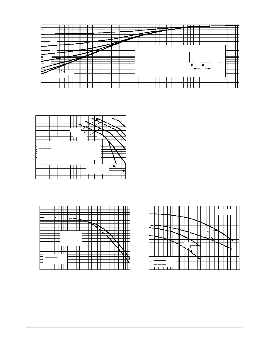
Figure 2. Switching Times Equivalent Circuit
5.0
0.1
Figure 3. Switching Times
IC, COLLECTOR CURRENT (AMP)
t, TIME
(s)
µ
2.0
1.0
0.5
0.05
0.2 0.3
0.5 0.7 1.0
2.0 3.0
10
0.3
0.7
tf
tr
ts
td @ VBE(off) = 0 V
V2
approx
+8.0 V
V1
approx
-12 V
tr, tf
10 ns
DUTY CYCLE = 1.0%
25
µ
s
0
RB
51
D1
+4.0 V
VCC
-30 V
RC
TUT
8.0 k
120
SCOPE
for td and tr, D1 is disconnected
and V2 = 0
For NPN test circuit reverse all polarities and D1.
RB & RC VARIED TO OBTAIN DESIRED CURRENT LEVELS
D1 MUST BE FAST RECOVERY TYPE, eg:
1N5825 USED ABOVE IB
100 mA
MSD6100 USED BELOW IB
100 mA
3.0
0.2
0.1
0.07
5.0 7.0
VCC = 30 V
IC/IB = 250
IB1 = IB2
TJ = 25
°
C
PNP
NPN
2N6040 2N6042 2N6043 2N6045
http://onsemi.com
3
Figure 4. Thermal Response
t, TIME OR PULSE WIDTH (ms)
1.0
0.01
0.01
0.5
0.2
0.1
0.05
0.02
r(t)
, EFFECTIVE
TRANSIENT
THERMAL
RESIST
ANCE (NORMALIZED)
0.05
0.1
0.2
0.5
1.0
2.0
5.0
10
20
50
100
200
1000
500
JC(t) = r(t)
JC
JC = 1.67
°
C/W
D CURVES APPLY FOR POWER
PULSE TRAIN SHOWN
READ TIME AT t1
TJ(pk) - TC = P(pk)
JC(t)
P(pk)
t1
t2
DUTY CYCLE, D = t1/t2
D = 0.5
0.2
0.05
0.02
0.1
0.7
0.3
0.07
0.03
0.02 0.03
0.3
3.0
30
300
SINGLE PULSE
0.01
20
1.0
Figure 5. ActiveRegion Safe Operating Area
VCE, COLLECTOR-EMITTER VOLTAGE (VOLTS)
10
5.0
2.0
1.0
0.02
2.0 3.0
7.0
50
100
BONDING WIRE LIMITED
THERMALLY LIMITED @ TC = 25
°
C
(SINGLE PULSE)
SECOND BREAKDOWN LIMITED
70
I C
, COLLECT
OR CURRENT
(AMP)
TJ = 150
°
C
dc
1.0 ms
100
µ
s
0.5
0.2
0.05
5.0
2N6040, 2N6043
2N6045
0.1
10
20
30
500
µ
s
5.0 ms
CURVES APPLY BELOW RATED VCEO
There are two limitations on the power handling ability of
a transistor: average junction temperature and second
breakdown. Safe operating area curves indicate IC VCE
limits of the transistor that must be observed for reliable
operation; i.e., the transistor must not be subjected to greater
dissipation than the curves indicate.
The data of Figure 5 is based on TJ(pk) = 150_C; TC is
variable depending on conditions. Second breakdown pulse
limits are valid for duty cycles to 10% provided TJ(pk)
< 150
_C. TJ(pk) may be calculated from the data in
Figure 4. At high case temperatures, thermal limitations will
reduce the power that can be handled to values less than the
limitations imposed by second breakdown.
300
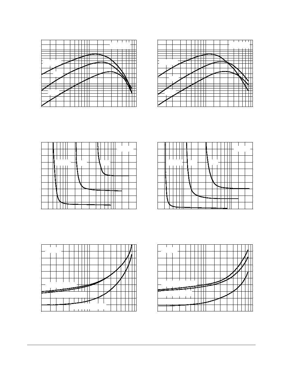
Figure 6. SmallSignal Current Gain
VR, REVERSE VOLTAGE (VOLTS)
30
0.5
1.0
2.0
100
5.0
0.1
0.2
C, CAP
ACIT
ANCE (pF)
200
70
50
TJ = 25
°
C
Cib
100
Cob
PNP
NPN
10,000
1.0
Figure 7. Capacitance
f, FREQUENCY (kHz)
10
2.0
5.0
20
50
1000
100
10
10
20
h fe
, SMALL-SIGNAL
CURRENT
GAIN
5000
3000
2000
1000
500
300
200
100
50
30
20
200
500
PNP
NPN
TC = 25
°
C
VCE = 4.0 Vdc
IC = 3.0 Adc
50
2N6040 2N6042 2N6043 2N6045
http://onsemi.com
4
V CE
, COLLECT
OR-EMITTER VOL
T
AGE (VOL
TS)
V CE
, COLLECT
OR-EMITTER VOL
T
AGE (VOL
TS)
20,000
0.1
Figure 8. DC Current Gain
IC, COLLECTOR CURRENT (AMP)
200
0.2 0.3
0.5
1.0
2.0
10
h FE
, DC CURRENT
GAIN
0.7
7.0
PNP
2N6040, 2N6042
NPN
2N6043, 2N6045
Figure 9. Collector Saturation Region
3.0
0.3
IB, BASE CURRENT (mA)
1.0
0.5
1.0
2.0
10
30
1.8
IC = 2.0 A
TJ = 25
°
C
4.0 A
2.2
2.6
0.7
5.0
3.0
0.1
IC, COLLECTOR CURRENT (AMP)
0.2 0.3
0.5 0.7 1.0
3.0
10
2.5
2.0
1.5
1.0
0.5
TJ = 25
°
C
VBE(sat) @ IC/IB = 250
VCE(sat) @ IC/IB = 250
V
,
VOL
T
AGE (VOL
TS)
VBE @ VCE = 4.0 V
2.0
10,000
TJ = 150
°
C
25
°
C
-55
°
C
20
IC, COLLECTOR CURRENT (AMP)
h FE
, DC CURRENT
GAIN
VCE = 4.0 V
TJ = 150
°
C
25
°
C
-55
°
C
1.4
6.0 A
IB, BASE CURRENT (mA)
TJ = 25
°
C
IC, COLLECTOR CURRENT (AMP)
V
,
VOL
T
AGE (VOL
TS)
7000
5000
3000
2000
1000
700
500
300
3.0
5.0
VCE = 4.0 V
20,000
0.1
200
0.2 0.3
0.5
1.0
2.0
10
0.7
7.0
10,000
7000
5000
3000
2000
1000
700
500
300
3.0
5.0
3.0
7.0
IC = 2.0 A
4.0 A
6.0 A
3.0
0.3
1.0
0.5
1.0
2.0
10
30
1.8
2.2
2.6
0.7
5.0
20
1.4
3.0
7.0
7.0
5.0
3.0
0.1
0.2 0.3
0.5 0.7 1.0
3.0
10
2.5
2.0
1.5
1.0
0.5
2.0
7.0
5.0
TJ = 25
°
C
VBE(sat) @ IC/IB = 250
VCE(sat) @ IC/IB = 250
VBE @ VCE = 4.0 V
Figure 10. "On" Voltages
2N6040 2N6042 2N6043 2N6045
http://onsemi.com
5
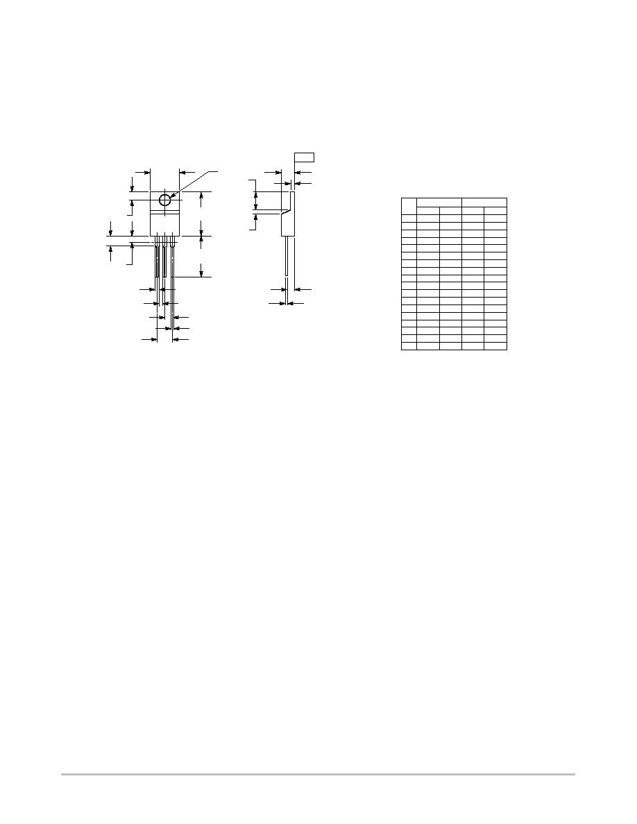
PACKAGE DIMENSIONS
CASE 221A09
ISSUE AA
TO220AB
NOTES:
1. DIMENSIONING AND TOLERANCING PER ANSI
Y14.5M, 1982.
2. CONTROLLING DIMENSION: INCH.
3. DIMENSION Z DEFINES A ZONE WHERE ALL
BODY AND LEAD IRREGULARITIES ARE
ALLOWED.
DIM
MIN
MAX
MIN
MAX
MILLIMETERS
INCHES
A
0.570
0.620
14.48
15.75
B
0.380
0.405
9.66
10.28
C
0.160
0.190
4.07
4.82
D
0.025
0.035
0.64
0.88
F
0.142
0.147
3.61
3.73
G
0.095
0.105
2.42
2.66
H
0.110
0.155
2.80
3.93
J
0.018
0.025
0.46
0.64
K
0.500
0.562
12.70
14.27
L
0.045
0.060
1.15
1.52
N
0.190
0.210
4.83
5.33
Q
0.100
0.120
2.54
3.04
R
0.080
0.110
2.04
2.79
S
0.045
0.055
1.15
1.39
T
0.235
0.255
5.97
6.47
U
0.000
0.050
0.00
1.27
V
0.045
---
1.15
---
Z
---
0.080
---
2.04
B
Q
H
Z
L
V
G
N
A
K
F
1 2 3
4
D
SEATING
PLANE
T
C
S
T
U
R
J
STYLE 1:
PIN 1. BASE
2. COLLECTOR
3. EMITTER
4. COLLECTOR