 | Электронный компонент: 2N6339 | Скачать:  PDF PDF  ZIP ZIP |
─εΩ≤∞σφ≥α÷Φ Φ ε∩Φ±αφΦ www.docs.chipfind.ru
High-Power NPN Silicon
Transistors
. . . designed for use in industrial¡military power amplifier and
switching circuit applications.
╖
High Collector¡Emitter Sustaining Voltage ¡
V
CEO(sus)
= 100 Vdc (Min) ¡ 2N6338
= 150 Vdc (Min) ¡ 2N6341
╖
High DC Current Gain ¡
h
FE
= 30 ¡ 120 @ I
C
= 10 Adc
= 12 (Min) @ I
C
= 25 Adc
╖
Low Collector¡Emitter Saturation Voltage ¡
V
CE(sat)
= 1.0 Vdc (Max) @ I
C
= 10 Adc
╖
Fast Switching Times @ I
C
= 10 Adc
t
r
= 0.3 ms (Max)
t
s
= 1.0 ms (Max)
t
f
= 0.25 ms (Max)
╬╬╬╬╬╬╬╬╬╬╬╬╬╬╬╬╬╬╬╬╬╬╬
╬╬╬╬╬╬╬╬╬╬╬╬╬╬╬╬╬╬╬╬╬╬╬
*MAXIMUM RATINGS
╬╬╬╬╬╬╬╬╬
╬╬╬╬╬╬╬╬╬
Rating
╬╬╬╬
╬╬╬╬
Symbol
╬╬╬╬╬╬
╬╬╬╬╬╬
2N6338
╬╬╬╬╬
╬╬╬╬╬
2N6341
╬╬╬
╬╬╬
Unit
╬╬╬╬╬╬╬╬╬
╬╬╬╬╬╬╬╬╬
Collector¡Base Voltage
╬╬╬╬
╬╬╬╬
V
CB
╬╬╬╬╬╬
╬╬╬╬╬╬
120
╬╬╬╬╬
╬╬╬╬╬
180
╬╬╬
╬╬╬
Vdc
╬╬╬╬╬╬╬╬╬
╬╬╬╬╬╬╬╬╬
Collector¡Emitter Voltage
╬╬╬╬
╬╬╬╬
V
CEO
╬╬╬╬╬╬
╬╬╬╬╬╬
100
╬╬╬╬╬
╬╬╬╬╬
150
╬╬╬
╬╬╬
Vdc
╬╬╬╬╬╬╬╬╬
Emitter¡Base Voltage
╬╬╬╬
V
EB
╬╬╬╬╬╬╬╬╬╬
6.0
╬╬╬
Vdc
╬╬╬╬╬╬╬╬╬
╬
╬╬╬╬╬╬╬
╬
╬╬╬╬╬╬╬╬╬
Collector Current
Continuous
Peak
╬╬╬╬
╬
╬╬
╬
╬╬╬╬
I
C
╬╬╬╬╬╬╬╬╬╬
╬
╬╬╬╬╬╬╬╬
╬
╬╬╬╬╬╬╬╬╬╬
25
50
╬╬╬
╬
╬
╬
╬╬╬
Adc
╬╬╬╬╬╬╬╬╬
╬╬╬╬╬╬╬╬╬
Base Current
╬╬╬╬
╬╬╬╬
I
B
╬╬╬╬╬╬╬╬╬╬
╬╬╬╬╬╬╬╬╬╬
10
╬╬╬
╬╬╬
Adc
╬╬╬╬╬╬╬╬╬
╬
╬╬╬╬╬╬╬
╬
╬╬╬╬╬╬╬╬╬
Total Device Dissipation
@ T
C
= 25
_
C
Derate above 25
_
C
╬╬╬╬
╬
╬╬
╬
╬╬╬╬
P
D
╬╬╬╬╬╬╬╬╬╬
╬
╬╬╬╬╬╬╬╬
╬
╬╬╬╬╬╬╬╬╬╬
200
1.14
╬╬╬
╬
╬
╬
╬╬╬
Watts
W/
░
C
╬╬╬╬╬╬╬╬╬
╬
╬╬╬╬╬╬╬
╬
╬╬╬╬╬╬╬╬╬
Operating and Storage Junction
Temperature Range
╬╬╬╬
╬
╬╬
╬
╬╬╬╬
T
J
, T
stg
╬╬╬╬╬╬╬╬╬╬
╬
╬╬╬╬╬╬╬╬
╬
╬╬╬╬╬╬╬╬╬╬
¡65 to +200
╬╬╬
╬
╬
╬
╬╬╬
_
C
╬╬╬╬╬╬╬╬╬╬╬╬╬╬╬╬╬╬╬╬╬╬╬
╬╬╬╬╬╬╬╬╬╬╬╬╬╬╬╬╬╬╬╬╬╬╬
THERMAL CHARACTERISTICS
╬╬╬╬╬╬╬╬╬╬╬╬
╬╬╬╬╬╬╬╬╬╬╬╬
Characteristic
╬╬╬╬╬
╬╬╬╬╬
Symbol
╬╬╬╬╬╬
╬╬╬╬╬╬
Max
╬╬╬
╬╬╬
Unit
╬╬╬╬╬╬╬╬╬╬╬╬
Thermal Resistance, Junction to Case
╬╬╬╬╬
JC
╬╬╬╬╬╬
0.875
╬╬╬
_
C/W
*Indicates JEDEC Registered Data.
200
75
50
25
0
0
25
50
75
100
125
150
175
200
Figure 1. Power Derating
T
C
, CASE TEMPERATURE (
░
C)
P D
, POWER DISSIP
A
TION (W
A
TTS)
175
150
125
100
Preferred devices are ON Semiconductor recommended choices for future use and best overall value.
ON Semiconductort
⌐
Semiconductor Components Industries, LLC, 2001
May, 2001 ¡ Rev. 10
1
Publication Order Number:
2N6338/D
2N6338
2N6341
*ON Semiconductor Preferred Device
25 AMPERE
POWER TRANSISTORS
NPN SILICON
100, 120, 140, 150 VOLTS
200 WATTS
*
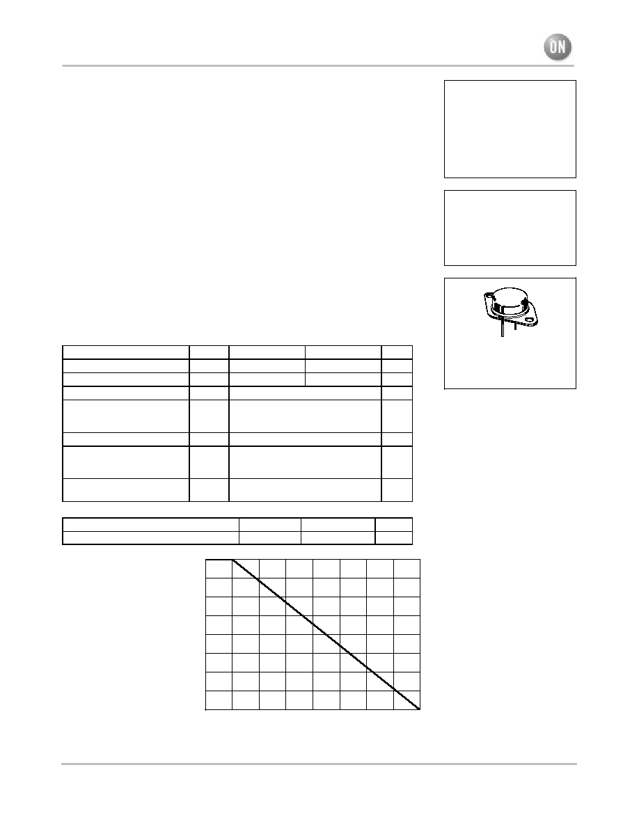
CASE 1¡07
TO¡204AA
(TO¡3)
2N6338 2N6341
http://onsemi.com
2
╬╬╬╬╬╬╬╬╬╬╬╬╬╬╬╬╬╬╬╬╬╬╬╬╬╬╬╬╬╬╬╬╬
╬╬╬╬╬╬╬╬╬╬╬╬╬╬╬╬╬╬╬╬╬╬╬╬╬╬╬╬╬╬╬╬╬
*ELECTRICAL CHARACTERISTICS
(T
C
= 25
_
C unless otherwise noted)
╬╬╬╬╬╬╬╬╬╬╬╬╬╬╬╬╬╬╬╬╬╬
╬╬╬╬╬╬╬╬╬╬╬╬╬╬╬╬╬╬╬╬╬╬
Characteristic
╬╬╬╬╬
╬╬╬╬╬
Symbol
╬╬╬
╬╬╬
Min
╬╬╬╬
╬╬╬╬
Max
╬╬╬
╬╬╬
Unit
╬╬╬╬╬╬╬╬╬╬╬╬╬╬╬╬╬╬╬╬╬╬╬╬╬╬╬╬╬╬╬╬╬
╬╬╬╬╬╬╬╬╬╬╬╬╬╬╬╬╬╬╬╬╬╬╬╬╬╬╬╬╬╬╬╬╬
OFF CHARACTERISTICS
╬╬╬╬╬╬╬╬╬╬╬╬╬╬╬╬╬╬╬╬╬╬
╬╬╬╬╬╬╬╬╬╬╬╬╬╬╬╬╬╬╬╬╬╬
Collector¡Emitter Sustaining Voltage (1)
2N6338
(I
C
= 50 mAdc, I
B
= 0)
2N6341
╬╬╬╬╬
╬╬╬╬╬
V
CEO(sus)
╬╬╬
╬╬╬
100
150
╬╬╬╬
╬╬╬╬
¡
¡
╬╬╬
╬╬╬
Vdc
╬╬╬╬╬╬╬╬╬╬╬╬╬╬╬╬╬╬╬╬╬╬
╬
╬╬╬╬╬╬╬╬╬╬╬╬╬╬╬╬╬╬╬╬
╬
╬
╬╬╬╬╬╬╬╬╬╬╬╬╬╬╬╬╬╬╬╬
╬
╬╬╬╬╬╬╬╬╬╬╬╬╬╬╬╬╬╬╬╬╬╬
Collector Cutoff Current
(V
CE
= 50 Vdc, I
B
= 0)
2N6338
(V
CE
= 75 Vdc, I
B
= 0)
2N6341
╬╬╬╬╬
╬
╬╬╬
╬
╬
╬╬╬
╬
╬╬╬╬╬
I
CEO
╬╬╬
╬
╬
╬
╬
╬
╬
╬╬╬
¡
¡
╬╬╬╬
╬
╬╬
╬
╬
╬╬
╬
╬╬╬╬
50
50
╬╬╬
╬
╬
╬
╬
╬
╬
╬╬╬
╡
Adc
╬╬╬╬╬╬╬╬╬╬╬╬╬╬╬╬╬╬╬╬╬╬
╬
╬╬╬╬╬╬╬╬╬╬╬╬╬╬╬╬╬╬╬╬
╬
╬╬╬╬╬╬╬╬╬╬╬╬╬╬╬╬╬╬╬╬╬╬
Collector Cutoff Current
(V
CE
= Rated V
CEO
, V
EB(off)
= 1.5 Vdc)
(V
CE
= Rated V
CEO
, V
EB(off)
= 1.5 Vdc, T
C
= 150
_
C)
╬╬╬╬╬
╬
╬╬╬
╬
╬╬╬╬╬
I
CEX
╬╬╬
╬
╬
╬
╬╬╬
¡
¡
╬╬╬╬
╬
╬╬
╬
╬╬╬╬
10
1.0
╬╬╬
╬
╬
╬
╬╬╬
╡
Adc
mAdc
╬╬╬╬╬╬╬╬╬╬╬╬╬╬╬╬╬╬╬╬╬╬
╬╬╬╬╬╬╬╬╬╬╬╬╬╬╬╬╬╬╬╬╬╬
Collector Cutoff Current (V
CB
= Rated V
CB
, I
E
= 0)
╬╬╬╬╬
╬╬╬╬╬
I
CBO
╬╬╬
╬╬╬
¡
╬╬╬╬
╬╬╬╬
10
╬╬╬
╬╬╬
╡
Adc
╬╬╬╬╬╬╬╬╬╬╬╬╬╬╬╬╬╬╬╬╬╬
╬╬╬╬╬╬╬╬╬╬╬╬╬╬╬╬╬╬╬╬╬╬
Emitter Cutoff Current (V
BE
= 6.0 Vdc, I
C
= 0)
╬╬╬╬╬
╬╬╬╬╬
I
EBO
╬╬╬
╬╬╬
¡
╬╬╬╬
╬╬╬╬
100
╬╬╬
╬╬╬
╡
Adc
╬╬╬╬╬╬╬╬╬╬╬╬╬╬╬╬╬╬╬╬╬╬╬╬╬╬╬╬╬╬╬╬╬
╬╬╬╬╬╬╬╬╬╬╬╬╬╬╬╬╬╬╬╬╬╬╬╬╬╬╬╬╬╬╬╬╬
ON CHARACTERISTICS (1)
╬╬╬╬╬╬╬╬╬╬╬╬╬╬╬╬╬╬╬╬╬╬
╬
╬╬╬╬╬╬╬╬╬╬╬╬╬╬╬╬╬╬╬╬
╬
╬
╬╬╬╬╬╬╬╬╬╬╬╬╬╬╬╬╬╬╬╬
╬
╬╬╬╬╬╬╬╬╬╬╬╬╬╬╬╬╬╬╬╬╬╬
DC Current Gain)
(I
C
= 0.5 Adc, V
CE
= 2.0 Vdc)
(I
C
= 10 Adc, V
CE
= 2.0 Vdc)
(I
C
= 25 Adc, V
CE
= 2.0 Vdc)
╬╬╬╬╬
╬
╬╬╬
╬
╬
╬╬╬
╬
╬╬╬╬╬
h
FE
╬╬╬
╬
╬
╬
╬
╬
╬
╬╬╬
50
30
12
╬╬╬╬
╬
╬╬
╬
╬
╬╬
╬
╬╬╬╬
¡
120
¡
╬╬╬
╬
╬
╬
╬
╬
╬
╬╬╬
¡
╬╬╬╬╬╬╬╬╬╬╬╬╬╬╬╬╬╬╬╬╬╬
╬
╬╬╬╬╬╬╬╬╬╬╬╬╬╬╬╬╬╬╬╬
╬
╬╬╬╬╬╬╬╬╬╬╬╬╬╬╬╬╬╬╬╬╬╬
Collector Emitter Saturation Voltage
(I
C
= 10 Adc, I
B
= 1.0 Adc)
(I
C
= 25 Adc, I
B
= 2.5 Adc)
╬╬╬╬╬
╬
╬╬╬
╬
╬╬╬╬╬
V
CE(sat)
╬╬╬
╬
╬
╬
╬╬╬
¡
¡
╬╬╬╬
╬
╬╬
╬
╬╬╬╬
1.0
1.8
╬╬╬
╬
╬
╬
╬╬╬
Vdc
╬╬╬╬╬╬╬╬╬╬╬╬╬╬╬╬╬╬╬╬╬╬
╬
╬╬╬╬╬╬╬╬╬╬╬╬╬╬╬╬╬╬╬╬
╬
╬╬╬╬╬╬╬╬╬╬╬╬╬╬╬╬╬╬╬╬╬╬
Base¡Emitter Saturation Voltage
(I
C
= 10 Adc, I
B
= 1.0 Adc)
(I
C
= 25 Adc, I
B
= 2.5 Adc)
╬╬╬╬╬
╬
╬╬╬
╬
╬╬╬╬╬
V
BE(sat)
╬╬╬
╬
╬
╬
╬╬╬
¡
¡
╬╬╬╬
╬
╬╬
╬
╬╬╬╬
1.8
2.5
╬╬╬
╬
╬
╬
╬╬╬
Vdc
╬╬╬╬╬╬╬╬╬╬╬╬╬╬╬╬╬╬╬╬╬╬
╬╬╬╬╬╬╬╬╬╬╬╬╬╬╬╬╬╬╬╬╬╬
Base¡Emitter On Voltage (I
C
= 10 Adc, V
CE
= 2.0 Vdc)
╬╬╬╬╬
╬╬╬╬╬
V
BE(on)
╬╬╬
╬╬╬
¡
╬╬╬╬
╬╬╬╬
1.8
╬╬╬
╬╬╬
Vdc
╬╬╬╬╬╬╬╬╬╬╬╬╬╬╬╬╬╬╬╬╬╬╬╬╬╬╬╬╬╬╬╬╬
╬╬╬╬╬╬╬╬╬╬╬╬╬╬╬╬╬╬╬╬╬╬╬╬╬╬╬╬╬╬╬╬╬
DYNAMIC CHARACTERISTICS
╬╬╬╬╬╬╬╬╬╬╬╬╬╬╬╬╬╬╬╬╬╬
╬╬╬╬╬╬╬╬╬╬╬╬╬╬╬╬╬╬╬╬╬╬
Current¡Gain ¡ Bandwidth Product (2)
(I
C
= 1.0 Adc, V
CE
= 10 Vdc, f
test
= 10 MHz)
╬╬╬╬╬
╬╬╬╬╬
f
T
╬╬╬
╬╬╬
40
╬╬╬╬
╬╬╬╬
¡
╬╬╬
╬╬╬
MHz
╬╬╬╬╬╬╬╬╬╬╬╬╬╬╬╬╬╬╬╬╬╬
╬╬╬╬╬╬╬╬╬╬╬╬╬╬╬╬╬╬╬╬╬╬
Output Capacitance (V
CB
= 10 Vdc, I
E
= 0, f = 0.1 MHz)
╬╬╬╬╬
╬╬╬╬╬
C
ob
╬╬╬
╬╬╬
¡
╬╬╬╬
╬╬╬╬
300
╬╬╬
╬╬╬
pF
╬╬╬╬╬╬╬╬╬╬╬╬╬╬╬╬╬╬╬╬╬╬╬╬╬╬╬╬╬╬╬╬╬
╬╬╬╬╬╬╬╬╬╬╬╬╬╬╬╬╬╬╬╬╬╬╬╬╬╬╬╬╬╬╬╬╬
SWITCHING CHARACTERISTICS
╬╬╬╬╬╬╬╬╬╬╬╬╬╬╬╬╬╬╬╬╬╬
╬╬╬╬╬╬╬╬╬╬╬╬╬╬╬╬╬╬╬╬╬╬
Rise Time (V
CC
80 Vdc, I
C
= 10Adc, I
B1
= 1.0 Adc, V
BE(off)
= 6.0 Vdc)
╬╬╬╬╬
╬╬╬╬╬
t
r
╬╬╬
╬╬╬
¡
╬╬╬╬
╬╬╬╬
0.3
╬╬╬
╬╬╬
╡
s
╬╬╬╬╬╬╬╬╬╬╬╬╬╬╬╬╬╬╬╬╬╬
╬╬╬╬╬╬╬╬╬╬╬╬╬╬╬╬╬╬╬╬╬╬
Storage Time (V
CC
80 Vdc, I
C
= 10 Adc, I
B1
= I
B2
= 1.0 Adc)
╬╬╬╬╬
╬╬╬╬╬
t
s
╬╬╬
╬╬╬
¡
╬╬╬╬
╬╬╬╬
1.0
╬╬╬
╬╬╬
╡
s
╬╬╬╬╬╬╬╬╬╬╬╬╬╬╬╬╬╬╬╬╬╬
Fall Time (V
CC
80 Vdc, I
C
= 10 Adc, I
B1
= I
B2
= 1.0 Adc)
╬╬╬╬╬
t
f
╬╬╬
¡
╬╬╬╬
0.25
╬╬╬
╡
s
*Indicates JEDEC Registered Data.
(1) Pulse Test: Pulse Width
v
300
╡
s, Duty Cycle
v
2.0%.
(2) f
T
= |h
fe
|
╖
f
test
.
Figure 2. Switching Time Test Circuit
1000
0.3
Figure 3. Turn¡On Time
I
C
, COLLECTOR CURRENT (AMP)
t, TIME
(ns)
500
100
70
50
10
0.5 0.7
2.0 3.0
7.0
30
+ 11 V
0
V
CC
SCOPE
R
B
10 OHMS
- 5.0 V
t
r
, t
f
v 10 ns
DUTY CYCLE = 1.0%
R
C
8.0 OHMS
20
30
5.0
20
10
╡
s
- 9.0 V
700
200
300
1.0
10
NOTE: For information on Figures 3 and 6, R
B
and R
C
were
varied to obtain desired test conditions.
+ 80 V
1N4933
t
d
@ V
BE(off)
= 6.0 V
V
CC
= 80 V
I
C
/I
B
= 10
T
J
= 25
░
C
t
r
2N6338 2N6341
http://onsemi.com
3
Figure 4. Thermal Response
t, TIME (ms)
1.0
0.01
0.01
0.7
0.5
0.3
0.2
0.1
0.07
0.05
0.03
0.02
0.02 0.03
r(t), EFFECTIVE
TRANSIENT
THERMAL
RESIST
ANCE (NORMALIZED)
0.05
0.1
0.2
0.5
1.0
2.0
5.0
10
20
50
100
200
1000
500
JC
= r(t)
JC
JC
= 0.875
░
C/W MAX
D CURVES APPLY FOR POWER
PULSE TRAIN SHOWN
READ TIME AT t
1
T
J(pk)
- T
C
= P
(pk)
JC
(t)
P
(pk)
t
1
t
2
DUTY CYCLE, D = t
1
/t
2
D = 0.5
SINGLE PULSE
0.2
0.05
0.1
0.02
0.01
0.3
3.0
30
300
100
2.0
Figure 5. Active Region Safe Operating Area
50
5.0
0.01
10
20
70
200
T
J
= 200
░
C
2N6338
2N6341
0.1
10
0.5
I C, COLLECT
OR CURRENT
(AMP)
V
CE
, COLLECTOR-EMITTER VOLTAGE (VOLTS)
20
0.2
50
100
200
╡
s
5.0 ms
1.0 ms
dc
2.0
0.02
0.05
1.0
3.0 5.0
30
7.0
BONDING WIRE LIMITED
THERMALLY LIMITED @
T
C
= 25
░
C (SINGLE PULSE)
SECOND BREAKDOWN
LIMITED CURVES APPLY
BELOW RATED V
CEO
There are two limitations on the power handling ability of
a transistor: average junction temperature and second
breakdown. Safe operating area curves indicate I
C
¡V
CE
limits of the transistor that must be observed for reliable
operation; i.e., the transistor must not be subjected to greater
dissipation than the curves indicate.
The data of Figure 5 is based on T
J(pk)
= 200
_C; T
C
is
variable depending on conditions. Second breakdown pulse
limits are valid for duty cycles to 10% provided T
J(pk)
v 200_C. T
J(pk)
may be calculated from the data in
Figure 4. At high case temperatures, thermal limitations will
reduce the power that can be handled to values less than the
limitations imposed by second breakdown.
5.0
0.3
Figure 6. Turn¡Off Time
I
C
, COLLECTOR CURRENT (AMP)
t, TIME
(s)
╡
2.0
1.0
0.5
0.3
0.2
0.1
0.07
0.05
0.5 0.7 1.0
2.0
5.0
10
20 30
V
CC
= 80 V
I
B1
= I
B2
I
C
/I
B
= 10
T
J
= 25
░
C
t
s
3.0
0.7
3.0
t
f
5000
0.1
Figure 7. Capacitance
V
R
, REVERSE VOLTAGE (VOLTS)
50
0.5
1.0
2.0
5.0
20
50 100
10
C, CAP
ACIT
ANCE (pF)
700
500
200
100
T
J
= 25
░
C
C
ib
C
ob
3000
2000
1000
70
300
0.2

2N6338 2N6341
http://onsemi.com
4
PACKAGE DIMENSIONS
NOTES:
1. DIMENSIONING AND TOLERANCING PER ANSI
Y14.5M, 1982.
2. CONTROLLING DIMENSION: INCH.
3. ALL RULES AND NOTES ASSOCIATED WITH
REFERENCED TO-204AA OUTLINE SHALL APPLY.
STYLE 1:
PIN 1. BASE
2. EMITTER
CASE: COLLECTOR
DIM
MIN
MAX
MIN
MAX
MILLIMETERS
INCHES
A
1.550 REF
39.37 REF
B
---
1.050
---
26.67
C
0.250
0.335
6.35
8.51
D
0.038
0.043
0.97
1.09
E
0.055
0.070
1.40
1.77
G
0.430 BSC
10.92 BSC
H
0.215 BSC
5.46 BSC
K
0.440
0.480
11.18
12.19
L
0.665 BSC
16.89 BSC
N
---
0.830
---
21.08
Q
0.151
0.165
3.84
4.19
U
1.187 BSC
30.15 BSC
V
0.131
0.188
3.33
4.77
A
N
E
C
K
¡T¡
SEATING
PLANE
2 PL
D
M
Q
M
0.13 (0.005)
Y
M
T
M
Y
M
0.13 (0.005)
T
¡Q¡
¡Y¡
2
1
U
L
G
B
V
H
CASE 1¡07
TO¡204AA (TO¡3)
ISSUE Z
ON Semiconductor and are trademarks of Semiconductor Components Industries, LLC (SCILLC). SCILLC reserves the right to make changes
without further notice to any products herein. SCILLC makes no warranty, representation or guarantee regarding the suitability of its products for any particular
purpose, nor does SCILLC assume any liability arising out of the application or use of any product or circuit, and specifically disclaims any and all liability,
including without limitation special, consequential or incidental damages. "Typical" parameters which may be provided in SCILLC data sheets and/or
specifications can and do vary in different applications and actual performance may vary over time. All operating parameters, including "Typicals" must be
validated for each customer application by customer's technical experts. SCILLC does not convey any license under its patent rights nor the rights of others.
SCILLC products are not designed, intended, or authorized for use as components in systems intended for surgical implant into the body, or other applications
intended to support or sustain life, or for any other application in which the failure of the SCILLC product could create a situation where personal injury or
death may occur. Should Buyer purchase or use SCILLC products for any such unintended or unauthorized application, Buyer shall indemnify and hold
SCILLC and its officers, employees, subsidiaries, affiliates, and distributors harmless against all claims, costs, damages, and expenses, and reasonable
attorney fees arising out of, directly or indirectly, any claim of personal injury or death associated with such unintended or unauthorized use, even if such claim
alleges that SCILLC was negligent regarding the design or manufacture of the part. SCILLC is an Equal Opportunity/Affirmative Action Employer.
PUBLICATION ORDERING INFORMATION
CENTRAL/SOUTH AMERICA:
Spanish Phone: 303¡308¡7143 (Mon¡Fri 8:00am to 5:00pm MST)
Email: ONlit¡spanish@hibbertco.com
Toll¡Free from Mexico: Dial 01¡800¡288¡2872 for Access ¡
then Dial 866¡297¡9322
ASIA/PACIFIC: LDC for ON Semiconductor ¡ Asia Support
Phone: 1¡303¡675¡2121 (Tue¡Fri 9:00am to 1:00pm, Hong Kong Time)
Toll Free from Hong Kong & Singapore:
001¡800¡4422¡3781
Email: ONlit¡asia@hibbertco.com
JAPAN: ON Semiconductor, Japan Customer Focus Center
4¡32¡1 Nishi¡Gotanda, Shinagawa¡ku, Tokyo, Japan 141¡0031
Phone: 81¡3¡5740¡2700
Email: r14525@onsemi.com
ON Semiconductor Website: http://onsemi.com
For additional information, please contact your local
Sales Representative.
2N6338/D
NORTH AMERICA Literature Fulfillment:
Literature Distribution Center for ON Semiconductor
P.O. Box 5163, Denver, Colorado 80217 USA
Phone: 303¡675¡2175 or 800¡344¡3860 Toll Free USA/Canada
Fax: 303¡675¡2176 or 800¡344¡3867 Toll Free USA/Canada
Email: ONlit@hibbertco.com
Fax Response Line: 303¡675¡2167 or 800¡344¡3810 Toll Free USA/Canada
N. American Technical Support: 800¡282¡9855 Toll Free USA/Canada
EUROPE: LDC for ON Semiconductor ¡ European Support
German Phone: (+1) 303¡308¡7140 (Mon¡Fri 2:30pm to 7:00pm CET)
Email: ONlit¡german@hibbertco.com
French Phone: (+1) 303¡308¡7141 (Mon¡Fri 2:00pm to 7:00pm CET)
Email: ONlit¡french@hibbertco.com
English Phone: (+1) 303¡308¡7142 (Mon¡Fri 12:00pm to 5:00pm GMT)
Email: ONlit@hibbertco.com
EUROPEAN TOLL¡FREE ACCESS*: 00¡800¡4422¡3781
*Available from Germany, France, Italy, UK, Ireland