⌐
Semiconductor Components Industries, LLC, 2000
November, 2000 ¡ Rev. 5
1
Publication Order Number:
2N7000/D
2N7000
Preferred Device
Small Signal MOSFET
200 mAmps, 60 Volts
N¡Channel TO¡92
MAXIMUM RATINGS
Rating
Symbol
Value
Unit
Drain Source Voltage
VDSS
60
Vdc
Drain¡Gate Voltage (RGS = 1.0 M
)
VDGR
60
Vdc
Gate¡Source Voltage
¡ Continuous
¡ Non¡repetitive (tp
50
╡
s)
VGS
VGSM
▒
20
▒
40
Vdc
Vpk
Drain Current
¡ Continuous
¡ Pulsed
ID
IDM
200
500
mAdc
Total Power Dissipation @ TC = 25
░
C
Derate above 25
░
C
PD
350
2.8
mW
mW/
░
C
Operating and Storage Temperature
Range
TJ, Tstg
¡55 to
+150
░
C
THERMAL CHARACTERISTICS
Characteristic
Symbol
Max
Unit
Thermal Resistance, Junction to
Ambient
R
JA
357
░
C/W
Maximum Lead Temperature for
Soldering Purposes, 1/16
from case
for 10 seconds
TL
300
░
C
2N7000
Y
= Year
WW
= Work Week
YWW
http://onsemi.com
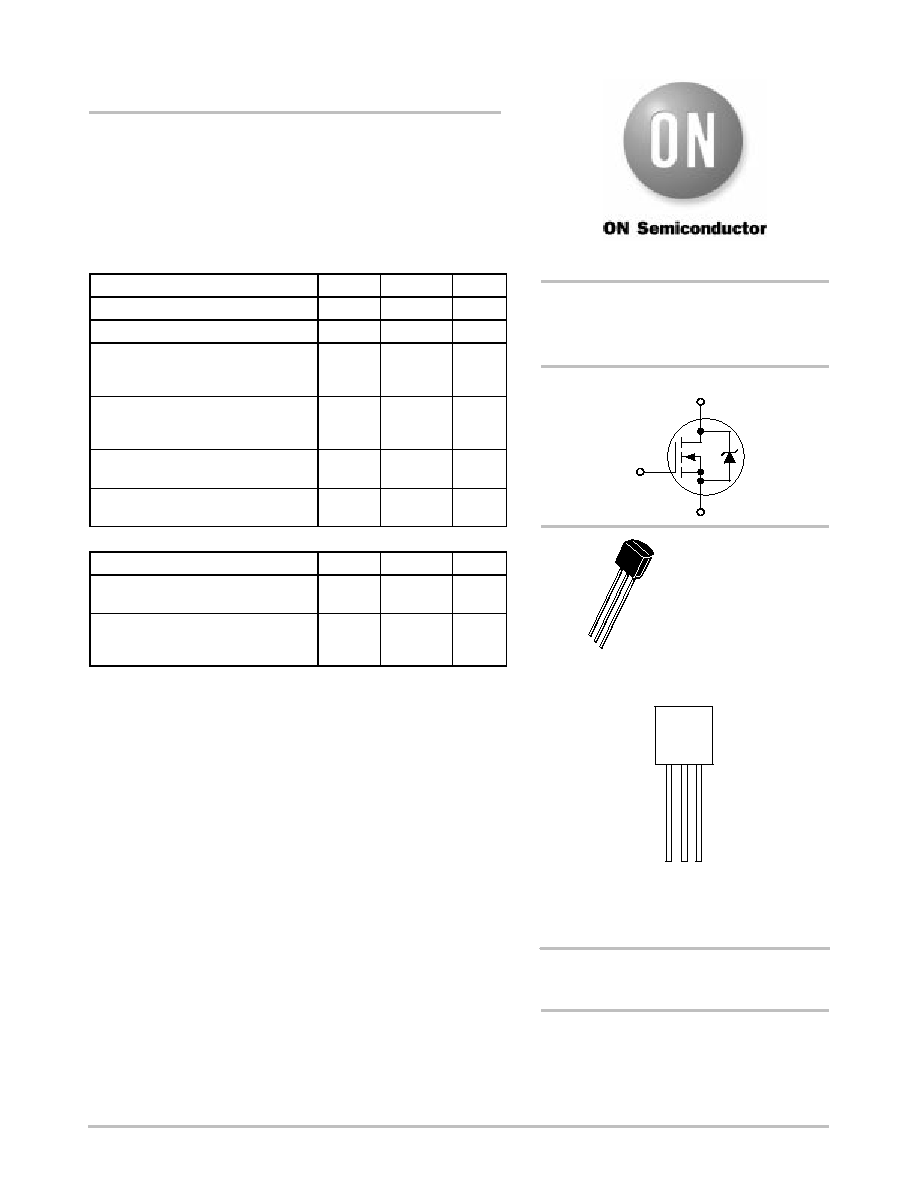
MARKING DIAGRAM
& PIN ASSIGNMENT
D
G
TO¡92
CASE 29
Style 22
N¡Channel
S
1 2
3
1
Source
3
Drain
2
Gate
200 mAMPS
60 VOLTS
RDS(on) = 5
Preferred devices are recommended choices for future use
and best overall value.
See detailed ordering and shipping information in the package
dimensions section on page 3 of this data sheet.
ORDERING INFORMATION

2N7000
http://onsemi.com
2
ELECTRICAL CHARACTERISTICS
(TC = 25
░
C unless otherwise noted)
Characteristic
Symbol
Min
Max
Unit
OFF CHARACTERISTICS
Drain¡Source Breakdown Voltage
(VGS = 0, ID = 10
╡
Adc)
V(BR)DSS
60
¡
Vdc
Zero Gate Voltage Drain Current
(VDS = 48 Vdc, VGS = 0)
(VDS = 48 Vdc, VGS = 0, TJ = 125
░
C)
IDSS
¡
¡
1.0
1.0
╡
Adc
mAdc
Gate¡Body Leakage Current, Forward
(VGSF = 15 Vdc, VDS = 0)
IGSSF
¡
¡10
nAdc
ON CHARACTERISTICS
(Note 1.)
Gate Threshold Voltage
(VDS = VGS, ID = 1.0 mAdc)
VGS(th)
0.8
3.0
Vdc
Static Drain¡Source On¡Resistance
(VGS = 10 Vdc, ID = 0.5 Adc)
(VGS = 4.5 Vdc, ID = 75 mAdc)
rDS(on)
¡
¡
5.0
6.0
Ohm
Drain¡Source On¡Voltage
(VGS = 10 Vdc, ID = 0.5 Adc)
(VGS = 4.5 Vdc, ID = 75 mAdc)
VDS(on)
¡
¡
2.5
0.45
Vdc
On¡State Drain Current
(VGS = 4.5 Vdc, VDS = 10 Vdc)
Id(on)
75
¡
mAdc
Forward Transconductance
(VDS = 10 Vdc, ID = 200 mAdc)
gfs
100
¡
╡
mhos
DYNAMIC CHARACTERISTICS
Input Capacitance
Ciss
¡
60
pF
Output Capacitance
(VDS = 25 V, VGS = 0,
f
1 0 MH )
Coss
¡
25
Reverse Transfer
Capacitance
( DS
,
GS
,
f = 1.0 MHz)
Crss
¡
5.0
SWITCHING CHARACTERISTICS
(Note 1.)
Turn¡On Delay Time
(VDD = 15 V, ID = 500 mA,
ton
¡
10
ns
Turn¡Off Delay Time
(VDD 15 V, ID 500 mA,
RG = 25
W
, RL = 30
W
, Vgen = 10 V)
toff
¡
10
1. Pulse Test: Pulse Width
300
╡
s, Duty Cycle
2.0%.

2N7000
http://onsemi.com
3
I D
, DRAIN CURRENT
(AMPS)
r DS(on)
, ST
A
TIC DRAIN-SOURCE ON-RESIST
ANCE
(NORMALIZED)
V GS(th)
,
THRESHOLD VOL
T
AGE (NORMALIZED)
I D
, DRAIN CURRENT
(AMPS)
2.0
1.8
1.6
1.4
1.2
1.0
0.8
0.6
0.4
0.2
0
10
0
1.0 2.0
3.0
4.0
5.0
6.0
7.0
8.0
9.0
VDS, DRAIN SOURCE VOLTAGE (VOLTS)
Figure 1. Ohmic Region
1.0
0.8
0.6
0.4
0.2
10
0
1.0 2.0
3.0
4.0
5.0
6.0
7.0
8.0
9.0
VGS, GATE SOURCE VOLTAGE (VOLTS)
Figure 2. Transfer Characteristics
2.4
2.2
2.0
1.8
1.6
1.4
1.2
1.0
0.8
0.6
0.4
1.2
1.05
1.1
1.10
1.0
0.95
0.9
0.85
0.8
0.75
0.7
-60
-20
+20
+60
+100
+140
-60
-20
+20
+60
+100
+140
T, TEMPERATURE (
░
C)
Figure 3. Temperature versus Static
Drain¡Source On¡Resistance
T, TEMPERATURE (
░
C)
Figure 4. Temperature versus Gate
Threshold Voltage
TA = 25
░
C
VGS = 10 V
9 V
8 V
7 V
6 V
4 V
3 V
5 V
VDS = 10 V
-55
░
C
25
░
C
125
░
C
VGS = 10 V
ID = 200 mA
VDS = VGS
ID = 1.0 mA
ORDERING INFORMATION
Device
Package
Shipping
2N7000
TO¡92
1000 Unit/Box
2N7000RLRA
TO¡92
2000 Tape & Reel
2N7000RLRM
TO¡92
2000 Ammo Pack
2N7000RLRP
TO¡92
2000 Ammo Pack
2N7000ZL1
TO¡92
2000 Ammo Pack
2N7000
http://onsemi.com
4
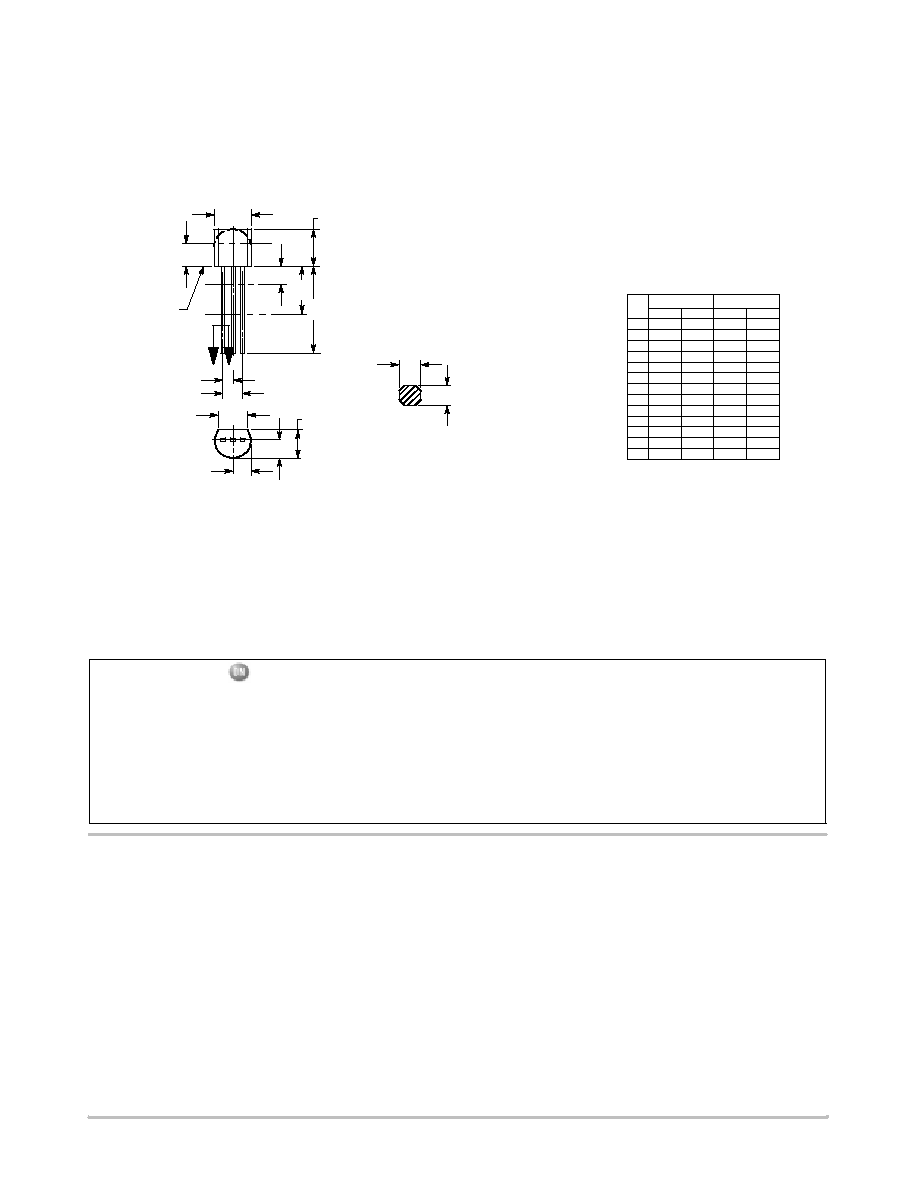
PACKAGE DIMENSIONS
STYLE 22:
PIN 1. SOURCE
2. GATE
3. DRAIN
NOTES:
1. DIMENSIONING AND TOLERANCING PER ANSI
Y14.5M, 1982.
2. CONTROLLING DIMENSION: INCH.
3. CONTOUR OF PACKAGE BEYOND DIMENSION R
IS UNCONTROLLED.
4. LEAD DIMENSION IS UNCONTROLLED IN P AND
BEYOND DIMENSION K MINIMUM.
R
A
P
J
L
B
K
G
H
SECTION X¡X
C
V
D
N
N
X X
SEATING
PLANE
DIM
MIN
MAX
MIN
MAX
MILLIMETERS
INCHES
A
0.175
0.205
4.45
5.20
B
0.170
0.210
4.32
5.33
C
0.125
0.165
3.18
4.19
D
0.016
0.021
0.407
0.533
G
0.045
0.055
1.15
1.39
H
0.095
0.105
2.42
2.66
J
0.015
0.020
0.39
0.50
K
0.500
---
12.70
---
L
0.250
---
6.35
---
N
0.080
0.105
2.04
2.66
P
---
0.100
---
2.54
R
0.115
---
2.93
---
V
0.135
---
3.43
---
1
TO¡92
CASE 29¡11
ISSUE AL
ON Semiconductor and are trademarks of Semiconductor Components Industries, LLC (SCILLC). SCILLC reserves the right to make changes
without further notice to any products herein. SCILLC makes no warranty, representation or guarantee regarding the suitability of its products for any particular
purpose, nor does SCILLC assume any liability arising out of the application or use of any product or circuit, and specifically disclaims any and all liability,
including without limitation special, consequential or incidental damages. "Typical" parameters which may be provided in SCILLC data sheets and/or
specifications can and do vary in different applications and actual performance may vary over time. All operating parameters, including "Typicals" must be
validated for each customer application by customer's technical experts. SCILLC does not convey any license under its patent rights nor the rights of others.
SCILLC products are not designed, intended, or authorized for use as components in systems intended for surgical implant into the body, or other applications
intended to support or sustain life, or for any other application in which the failure of the SCILLC product could create a situation where personal injury or
death may occur. Should Buyer purchase or use SCILLC products for any such unintended or unauthorized application, Buyer shall indemnify and hold
SCILLC and its officers, employees, subsidiaries, affiliates, and distributors harmless against all claims, costs, damages, and expenses, and reasonable
attorney fees arising out of, directly or indirectly, any claim of personal injury or death associated with such unintended or unauthorized use, even if such claim
alleges that SCILLC was negligent regarding the design or manufacture of the part. SCILLC is an Equal Opportunity/Affirmative Action Employer.
PUBLICATION ORDERING INFORMATION
CENTRAL/SOUTH AMERICA:
Spanish Phone: 303¡308¡7143 (Mon¡Fri 8:00am to 5:00pm MST)
Email: ONlit¡spanish@hibbertco.com
Toll¡Free from Mexico: Dial 01¡800¡288¡2872 for Access ¡
then Dial 866¡297¡9322
ASIA/PACIFIC: LDC for ON Semiconductor ¡ Asia Support
Phone: 303¡675¡2121 (Tue¡Fri 9:00am to 1:00pm, Hong Kong Time)
Toll Free from Hong Kong & Singapore:
001¡800¡4422¡3781
Email: ONlit¡asia@hibbertco.com
JAPAN: ON Semiconductor, Japan Customer Focus Center
4¡32¡1 Nishi¡Gotanda, Shinagawa¡ku, Tokyo, Japan 141¡0031
Phone: 81¡3¡5740¡2700
Email: r14525@onsemi.com
ON Semiconductor Website: http://onsemi.com
For additional information, please contact your local
Sales Representative.
2N7000/D
NORTH AMERICA Literature Fulfillment:
Literature Distribution Center for ON Semiconductor
P.O. Box 5163, Denver, Colorado 80217 USA
Phone: 303¡675¡2175 or 800¡344¡3860 Toll Free USA/Canada
Fax: 303¡675¡2176 or 800¡344¡3867 Toll Free USA/Canada
Email: ONlit@hibbertco.com
Fax Response Line: 303¡675¡2167 or 800¡344¡3810 Toll Free USA/Canada
N. American Technical Support: 800¡282¡9855 Toll Free USA/Canada
EUROPE: LDC for ON Semiconductor ¡ European Support
German Phone: (+1) 303¡308¡7140 (Mon¡Fri 2:30pm to 7:00pm CET)
Email: ONlit¡german@hibbertco.com
French Phone: (+1) 303¡308¡7141 (Mon¡Fri 2:00pm to 7:00pm CET)
Email: ONlit¡french@hibbertco.com
English Phone: (+1) 303¡308¡7142 (Mon¡Fri 12:00pm to 5:00pm GMT)
Email: ONlit@hibbertco.com
EUROPEAN TOLL¡FREE ACCESS*: 00¡800¡4422¡3781
*Available from Germany, France, Italy, UK, Ireland