 | –≠–ª–µ–∫—Ç—Ä–æ–Ω–Ω—ã–π –∫–æ–º–ø–æ–Ω–µ–Ω—Ç: AND8079D | –°–∫–∞—á–∞—Ç—å:  PDF PDF  ZIP ZIP |
©
Semiconductor Components Industries, LLC, 2002
October, 2002 - Rev. 1
1
Publication Order Number:
AND8079/D
AND8079/D
A Low Cost DDR Memory
Power Supply Using the
NCP1571 Synchronous Buck
Converter and a LM358
Based Linear Voltage
Regulator
Prepared by: Jim Lepkowski
Senior Application Engineer
INTRODUCTION
This application note describes a low cost power supply
circuit for a DDR (Double Data Rate) memory system. The
design is based on the NCP1570/NCP1571 low voltage
synchronous buck converter. The reference design created
to evaluate the system uses a 3.80
by 2.15
two layer printed
circuit board, optimized for a small solution size at an
economical cost.
DDR memories bring new challenges to the power supply
by requiring an efficient main power of 2.5 V (V
dd
) and a
second voltage (V
tt
) that accurately tracks one half of V
dd
(i.e. 1.25 V) that is capable of both sourcing and sinking
current. In addition, a third voltage is required (V
REF
) that
also tracks V
dd
/2. A low voltage synchronous buck
converter is used to create an 8.0 A output at 2.5 V, while the
V
tt
and V
REF
voltages are created using a unique operational
amplifier linear regulator circuit. The demonstration circuit
is designed for low power DDR systems such as desktop
PCs, but the circuit's output power capability can be
increased with the selection of the external inductor and
capacitors for high power systems such as PC workstations.
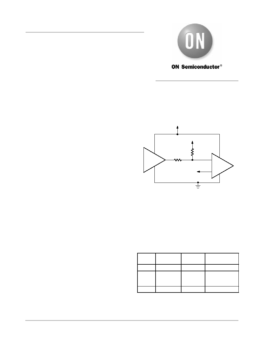
DDR Memory Power Supply Requirements
Figure 1 shows a simplified schematic of the DDR
memory system. Voltage V
dd
powers the memory ICs, in
addition to the buffer interface circuits. The termination
voltage V
tt
is used for the pull-up resistors and must be able
to either sink or source current. For example, if all of the
driver circuits are at a logic high state (i.e. V
OH
= V
dd
=
2.5 V), the Vtt supply will have to sink current in order to
maintain its 1.25 V. In contrast, if all of the driver circuits are
at a logic low state (i.e. V
OL
= V
ss
= 0 V), the Vtt supply will
have to source current because the termination resistors will
be effectively connected to ground.
Figure 1. DDR Memory Simplified Schematic
V
dd
RS
22
V
tt
= V
dd
/2
Transmitter
RT
25
Receiver
V
REF
V
tt
is equal to V
dd
/2 instead of V
dd
in order to save power.
The power dissipated in the resistors is equal to voltage
squared divided by the bus resistance, thus a termination
voltage of V
dd
/2 provides a factor of four power savings.
The third voltage is used as a reference voltage to the
differential amplifier input section of the receiver ICs.
A summary of the specifications for the DDR memory
system is listed below. The transient requirements are not
defined in the industry JEDEC standards.
DDR
Voltage
Output
Voltage
Tolerance
Output Current
V
dd
2.5 V
"
200 mV
8.0 A
V
tt
V
dd
/2
(
^
1.25 V)
V
dd
/2
"
3%
(1.250 V
"
37.5 mV)
"
2.0 A
(Sink and Source)
V
REF
V
dd
/2
V
tt
"
40 mV
5.0 mA
APPLICATION NOTE
http://onsemi.com

AND8079/D
http://onsemi.com
2
Many industry experts have predicted that DDR memory
will soon become the standard for desktop computers, with
notebooks shortly behind. Next generation DDR-II
generation
systems are likely to have a lower V
dd
voltage of
1.8 V with a V
tt
and V
REF
voltage equal to 900 mV. This
lower voltage will be required to satisfy the consumer's
requirement for more memory without a large increase in
required power.
Supply Voltage (V
dd
)
The V
dd
2.5 V power supply is created with the NCP1571
low voltage synchronous buck controller. The NCP1571
controller contains the required circuitry for a synchronous
N-channel MOSFET buck regulator. The V
2
t
control
method is used to achieve a fast 200 ns transient response
and an output regulation of
±
1.0%. The IC operates at a fixed
internal frequency of 200 kHz. In addition, the NCP1571
provides the following features: undervoltage lockout
protection, programmable soft start, power good signal with
delay and overvoltage protection. Note the NCP1570 and
NCP1571 are functionally and pin for pin equivalent. The
NCP1571's under voltage lockout operation (UVLO)
feature has been modified for applications that require a
parallel standby power supply in addition to the main power
supplied by the buck converter.
Termination Supply Voltage (V
tt
) and Reference
Voltage (V
REF
)
The V
tt
supply voltage is equal to one half of the Vdd
voltage, or approximately 1.25 V. Operational amplifiers
U
2A
and U
2B
function as voltage followers to create the V
tt
voltage. The input to U
2B
is created by the resistive voltage
divider formed by R
5
and R
6
and divides the 2.5 V V
dd
supply by two to form the V
REF
reference voltage. Also, U
2B
provides filtering to remove any of the high frequency
switching noise that is results from the synchronous buck
converter. The V
tt
output of the circuit formed by U
2A
and
transistors Q
4
and Q
5
tracks the voltage at the non-inverting
terminal by virtue of the voltage follower circuit
configuration. Thus, the output of voltage of the V
tt
supply
is referenced to 50% of the 2.5 V V
dd
supply, rather than an
absolute 1.25 V reference.
The sink and source ability of the V
tt
supply is provided
by MOSFETs Q
4
and Q
5
which are used to extend the
current capability of the operational amplifier circuit. When
the V
tt
supply is in the current sinking mode of operation, Q
4
is "OFF" and Q
5
is "ON". The output of U
2A
will be at a
negative voltage (i.e. ≠5.0 V) to control the V
gs
of the
P-channel MOSFET (Q
5
) in order to maintain the V
tt
voltage of 1.25 V. In a similar manner, when the V
tt
supply
is in the current sourcing mode of operation, Q
4
is "ON" and
Q
5
is "OFF". The output of U
2A
will reach a positive voltage
(i.e. + 4.5 V) to control the V
gs
of the N-channel MOSFET
(Q
5
) in order to maintain the V
tt
voltage of 1.25 V. Resistor
R
7
is used to isolate the output of U
2B
from V
tt
and the bulk
capacitor C
20
.
The slew rate of the operational amplifier and the ability
of the bulk capacitors to hold the voltage at 1.25 V under the
load conditions control the transient response of the V
tt
control loop. Note that the bulk capacitors maintain the V
tt
voltage at approximately 1.25 V; therefore, the operational
amplifier is only required to slew its output a relatively small
amount; therefore, the relatively slow slew rate of the
LM358 operational amplifiers is not a limiting factor in the
design.
Standby Power Operation
The demonstration PCB has the provision of providing a
low power standby mode of operation to the DDR memory
system. This mode could be used to provide a 2.5 V low
current standby voltage to the memory ICs when the main
5.0 V input power is not available. A MC33375 (U
3
)
300 mA low dropout voltage regulator (LDO) was chosen
for the design to provide the 2.5 V standby power. The
MC33375 has an ON/OFF enable pin and is available in a
SOT-223 package. The performance of the standby
regulator was not verified.
Q
1
, a N-Channel MOSFET, serves as a diode to prevent
current flow back to the main 5.0 volt input power supply
during the standby mode. The MOSFET was chosen instead
of a Schottky diode in order to minimize the voltage drop
and power consumption of the diode.
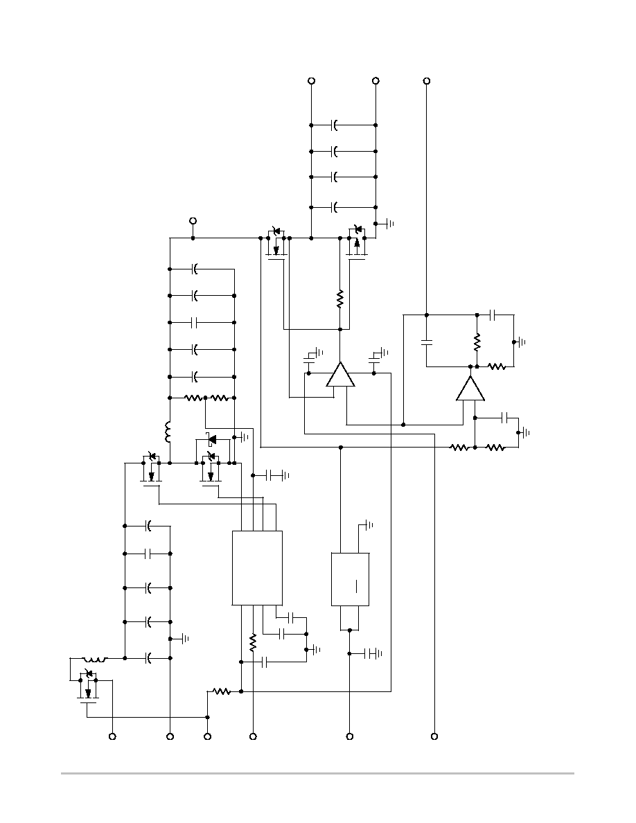
AND8079/D
http://onsemi.com
3
Q1
MTB1306
D2 PAK
TP5
TP6
TP7
TP8
TP9
TP10
5 V_Input
GND_Input
12 V_Input
V_Logic
V_5P0_STBV
-12 V_Input
R1
10
C12
0.1
m
F
VTT (+1.25V, 2A)
VREF (+1.25V, 2mA)
VDDQ (+2.5V, 8A)
Q2
MTB1306
D2 PAK
NCP1571
SO-8
L1
1
m
H
Q5
MTD20P03HDL
DPAK
C16
C17
VCC
GATE(H)
8
7
6
5
1
2
3
4
C1
1800
m
F
10V
C2
1800
m
F
10V
C4
0.1
m
F
C5
1800
m
F
10V
Prov.
C7
1800
m
F
6.3V
Prov.
C8
1800
m
F
6.3V
C9
0.1
m
F
C11
1800
m
F
6.3V
D1
MBRM110LT
PowerMite Prov.
C15
1
m
F
OUT
OUT
Q4
NTD4302
D2 PAK
TP1
TP2
TP3
TP4
Tol. = 1.0%
Tol. = 1.0%
U2A
LM358
Micro8
ON OFF
VOUT
C24
1
m
F
C20
1800
m
F
6.3V
Prov.
R7
1k
R5
10K
C21
1800
m
F
6.3V
Prov.
R6
10K
C22
0.1
m
F
C23
1800
m
F
6.3V
C18
0.15
m
F
R9
100
R8
200
C19
1.25V_Ref
GND_Output
1.25V_Vtt
6
5
7
R3
20k
R4
13k
L2
2.2
m
H
Tol = 1.0%
To = 1.0%
Q3
MTB1306
D2PAK
C6
100pF
2.5V
0.1
m
F
0.1
m
F
2
3
4
V-
V+
8
R2
47k
C13
0.01
m
F
C14
0.1
m
F
MC33375ST-2.5T3
SOT-223
1
2
3
4
U2B
LM358
C3
1800
m
F
10V
GATE(L)
Vfb
GND
PWRGD
PGDELAY
COMP
C10
1800
m
F
6.3V
GND
VIN
Figure 2. DDR Memory Reference Design
4
2
m
F
Note: The provisional components were not used in the verification of the reference design.
U1
U3 Prov.
-
+
-
+
1

AND8079/D
http://onsemi.com
4
Component Selection
Input Inductor
The input inductor (L
IN
) is used to isolate the input power
supply from the switching portion of the buck regulator. L
IN
also limits the inrush current into the bulk input capacitors
and limits the input current slew rate that results from the
transient load. The inductor blocks the ripple current and
transfers the transient current requirement to the bulk input
capacitor bank.
The design equations for L
IN
are listed below and for
connivance an inductance of 1.0
mH is chosen. The cut-off
frequency of the second order LC filter provides adequate
attenuation for the 200 kHz switching frequency of the
NCP1571.
LIN
+
D
V
(dI dt)Max
+
5 V
*
2.5 V
10 A
5
m
s
+
1.25
m
H
f
*
3db
+
1
2
p
LIN CIN
+
1
2
p
1
m
H
5400
m
F
+
216 Hz
where:
L
IN
= input inductor
C
IN
= bulk input capacitor(s)
dI/dt = 10 A in 5.0
ms
Input Capacitors
The input filter capacitors provide a charge reservoir that
minimizes the supply voltage variations due to the pulsating
current through the MOSFETs. The input capacitors are
chosen primarily to meet the ripple current rating of the
capacitors.
The design equation is listed below.
ICin(RMS)
+
D
(1
*
D)
Iout2
+
.5
(1
*
.5)
102
+
5 A
where:
D = duty cycle = V
OUT
/V
IN
= 2.5 V/5.0 V = 0.5
I
OUT
= maximum output current
The Rubycon 10 V 1800
mf capacitors have a ripple
current rating of 2.55 A. Thus only 2 of the capacitors are
needed to meet the ripple requirements; however, 3
capacitors were chosen to be conservative.
Output Inductance
The main criterion in selecting the output filter inductance
(L
OUT
) is to provide a satisfactory response to the load
transients. The inductance affects the output voltage ripple
by limiting the rate at which the current can either increase
or decrease. The design equation used for selecting L
OUT
is
listed below. A 2.2
mH inductor was chosen for the design.
LOUT
+
(VIN
*
VOUT)
tr
D
I
+
(5 V
*
2.5 V)
10
m
s
10 A
+
2.5
m
H
where:
tr = output transient load time
Output Capacitors
The output capacitors are selected to meet the desired
output ripple requirements. The key specifications for the
capacitors are their ESR (Equivalent Series Resistance) and
ESL (Equivalent Series Inductance). In order to obtain a
good transient response, a combination of low value/high
frequency ceramic capacitors and bulk electrolytic
capacitors are placed as close to the load as possible.
The voltage change during the load current transient is:
D
VOUT
+ D
IOUT
ESL
D
t
)
ESR
)
tr
COUT
^ D
IOUT
ESR
Empirical data indicates that most of the output voltage
change that results from the load current transients is
determined by the capacitor ESR; therefore, the maximum
allowable ESR can be approximated from the following
equation.
ESR max
^
D
VOUT
D
IOUT
+
75 mV
10 A
+
7.5 m
W
The number of capacitors is calculated by using the
equation listed below.
Number of capacitors
+
ESRCAP
ESR max
+
19 m
W
7.5 m
W +
2.5
The ESR of the Rubycon 6.3 V 1800
mF capacitors is
specified at 19 m
W; therefore, 3 capacitors are used in the
design.
MOSFET Selection
The output switch MOSFETs are chosen based on the gate
charge/gate-source threshold voltage, gate capacitance, on
resistance, current rating and the thermal capacity of the
package. In this DDR design, the MOSFETs were chosen for
economical reasons and have a current and power rating that
is much better than needed for this design. In addition, the
MOSFETs selected were verified by measuring the thermal
characteristics of the devices on the PCB.
The power dissipation design equation for selecting the
MOSFETs is given below.
P
+
IMAX2
RDS(ON)
D
)
IMAX
VDS
Tr
FS
2
)
IMAX
VDS
Tf
FS
2
where:
T
r
= rise time or turn-on time of MOSFET
T
f
= fall time or turn-off time of MOSFET
F
S
= switching frequency
AND8079/D
http://onsemi.com
5
Schottky Diode for Synchronous MOSFET
The efficiency of the buck converter can be improved
slightly by placing a Schottky diode (D
1
) in parallel with the
bottom MOSFET (Q
3
). The body diode of Q
3
is used to
conduct current during the non-overlap time when both the
top (Q
2
) and bottom (Q
3
) MOSFETs are turned OFF. But
because the non-overlap time is only approximately 50 ns
for the NCP1571's 200 kHz switching speed, the efficiency
savings will be only approximately 1.0%. The
demonstration board included a provision for D
1
; however,
the performance of the circuit was not testing with this
diode.
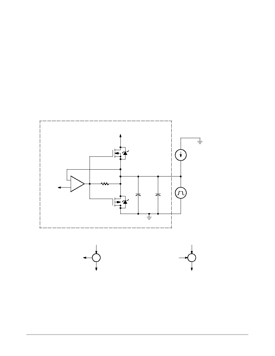
Experimental Results
The experimental results of the demonstration PCB are
shown in Figures 4 through 20. Figure 3 shows the test setup
used to create the current load transients for the V
tt
supply
voltage. The transient current load tests for the V
dd
and V
tt
supply voltages were created using a Kikusui Electronic
Load Controller. Unless noted, the standard test conditions
are as listed below:
1. Ambient Temperature = 23
_C
2. V
dd
Current Load (I
Vdd
) = 8.0 A
3. V
tt
Current Load (I
Vtt
) = 1.25 A source load
4. V
REF
Current Load (I
REF
) = 2.5 mA
5. 5.0 V Input Voltage = 5.00 V
6. 12 V Input Voltage = 12.00 V
7. -12 V Input Voltage = -12.00 V
Figure 3. V
tt
Transient Load Test Setup for a 2.0 A Sink to 2.0 A Source Test
2.5 V
V
dd
R7
OUT
-
+
-
-
+
Q4
U2A
V
REF
Q5
C22
+
C23
+
V
tt
V
tt
DDR Circuit
2.0 A
DC Current Source
Pulsating Current Source
Pulse Width = 100 ms
Period = 200 ms
l1 = 0 A
l2 = 4.0 A
Rise Time = 50
m
s
Fall Time
= 50
m
s
V
tt
Circuit
DC Current Source
Pulsating Current Source
0 A
2 .0 A
2.0 A
V
tt
2.0 A Current Sink Test
V
tt
Circuit
DC Current Source
Pulsating Current Source
4 A
V
tt
2.0 A Current Source Test
2 .0 A
2.0 A
+
AND8079/D
http://onsemi.com
6
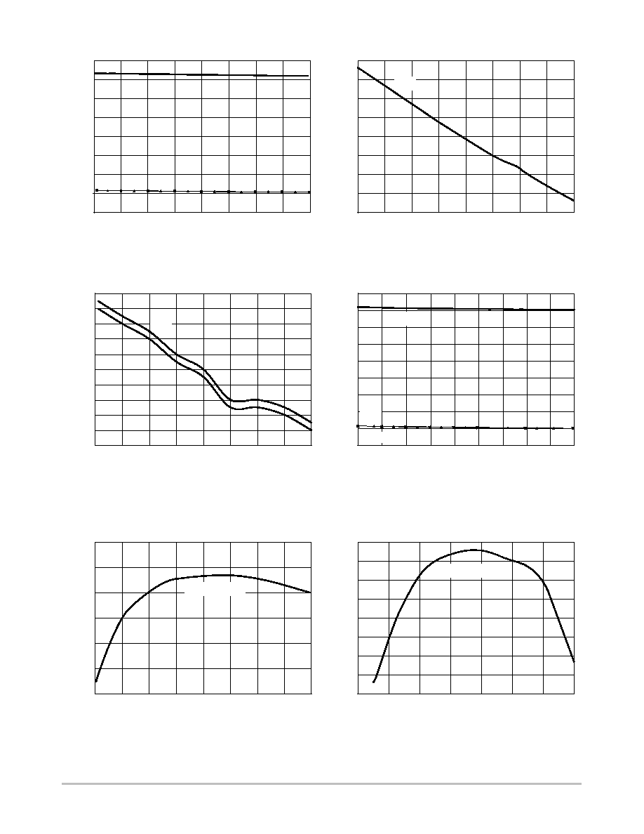
1.0
1.2
1.4
1.6
1.8
2.0
2.2
2.4
2.6
2.440
2.445
2.450
2.455
2.460
2.465
2.470
2.475
Figure 4. Output Voltage vs. V
dd
Load
Figure 5. V
dd
Voltage vs. V
dd
Load
Figure 6. V
tt
and V
ref
vs. V
dd
Load
1.214
1.216
1.218
1.220
1.222
1.224
1.226
1.228
1.230
1.232
1.234
0
1.0
2.0
3.0
4.0
5.0
6.0
7.0
8.0
1.0
1.2
1.4
1.6
1.8
2.0
2.2
2.4
2.6
3.5
4.0
4.5
5.0
5.5
6.0
6.5
7.0
7.5
8.0
Figure 7. Output Voltage vs. Input Voltage
Figure 8. Efficiency vs. V
dd
Load
Figure 9. Efficiency vs. Input Voltage
0.60
0.65
0.70
0.75
0.80
0.85
0.90
0
1
2
3
4
5
6
7
8
0.75
0.76
0.77
0.78
0.79
0.80
0.81
0.82
3
4
5
6
7
8
9
10
0.74
INPUT VOLTAGE (V)
EFFICIENCY (%)
EFFICIENCY
V
dd
LOAD CURRENT (A)
EFFICIENCY (%)
INPUT VOLTAGE (V)
VOL
T
AGE OUTPUT (V)
V
dd
LOAD (A)
EFFICIENCY
V
dd
VOL
T
AGE (V) V
tt
& V
ref
V
tt
V
ref
V
dd
LOAD (A)
OUTPUT VOL
T
AGE (V)
V
dd
LOAD (A)
V
dd
VOL
T
AGE (V)
0
1.0
2.0
3.0
4.0
5.0
6.0
7.0
8.0
V
dd
0
1.0
2.0
3.0
4.0
5.0
6.0
7.0
8.0
V
dd
J
V
tt
Y
V
ref
J
V
tt
Y
V
ref
AND8079/D
http://onsemi.com
7
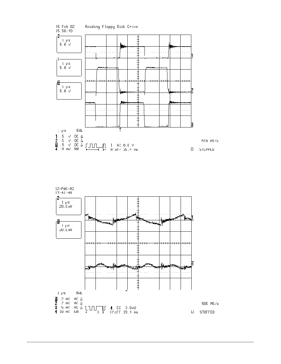
Figure 10. L
2
Inductor Voltage, Top (Q
2
) and Bottom (Q
3
) Buck MOSFET Gate Drive
Channel 1: L
2
Inductor Voltage
Channel 2: Bottom (Q
3
) Buck MOSFET Gate Drive
Channel 3: Top (Q
2
) Buck MOSFET Gate Drive
Figure 11. Steady-State V
dd
and V
tt
with I
Vdd
= 0.1 A, I
Vtt
= 1.25 A Sourcing and V
REF
= 2.45 mA
Channel 1: V
dd
ripple voltage
Channel 2: V
tt
ripple voltage
AND8079/D
http://onsemi.com
8
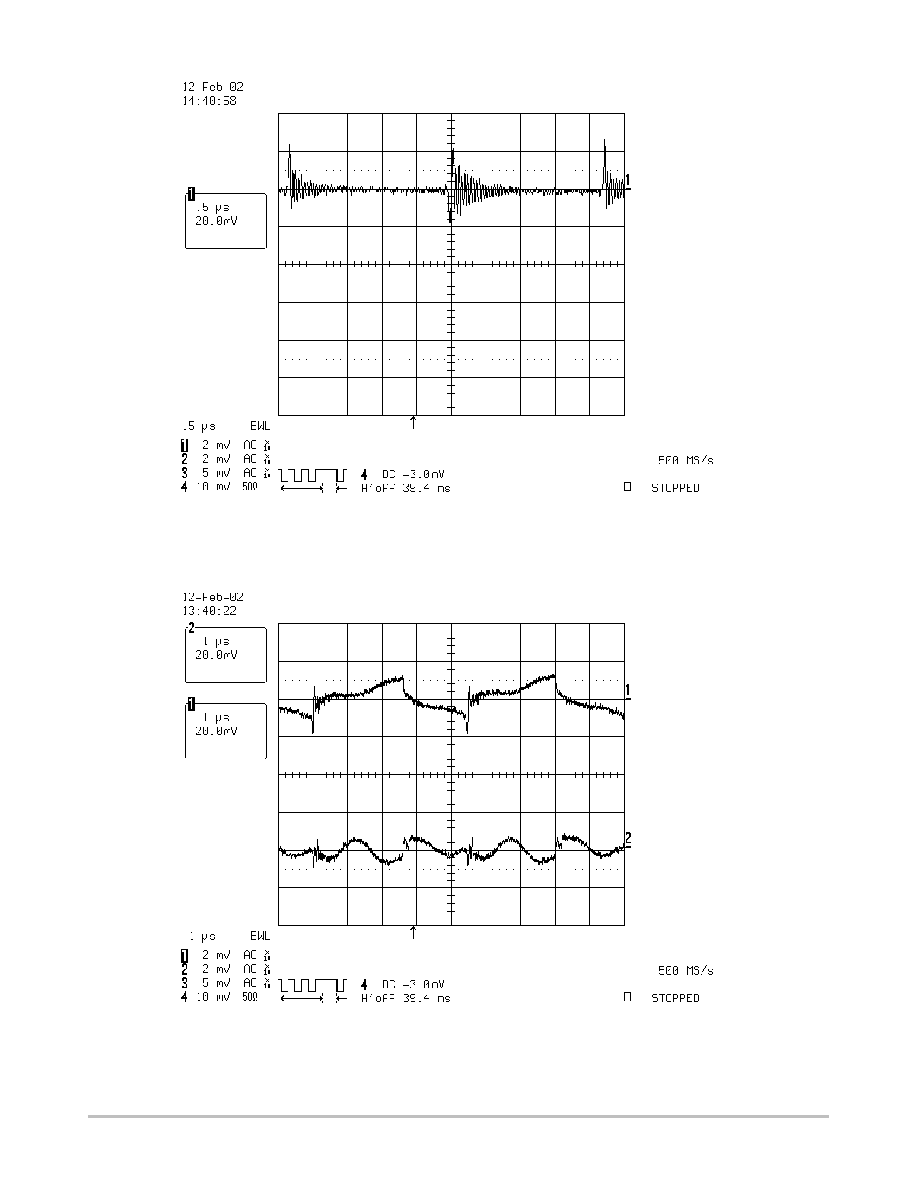
Figure 12. Steady-State V
REF
with I
Vdd
= 0.1 A, I
Vtt
= 1.25 A Sourcing and V
REF
= 2.45 mA
Channel 1: V
REF
ripple voltage
Figure 13. Steady-State V
dd
and V
tt
with I
Vdd
= 8.0 A, I
Vtt
= 1.25 A Sourcing and V
REF
= 2.45 mA
Channel 1: V
dd
ripple voltage
Channel 2: V
tt
ripple voltage
AND8079/D
http://onsemi.com
9
Figure 14. Steady-State V
REF
with I
Vdd
= 8.0 A, I
Vtt
= 1.25 A Sourcing and V
REF
= 2.45 mA
Channel 1: V
REF
ripple voltage
Figure 15. V
dd
with a Transient Load I
Vdd
= 0 to 8.0 A, I
Vtt
= 1.25 A Sourcing and V
REF
= 2.45 mA
Channel 1: V
dd
ripple voltage
Channel 2: Transient current load I
Vdd
= 0 to 8.0 A
AND8079/D
http://onsemi.com
10
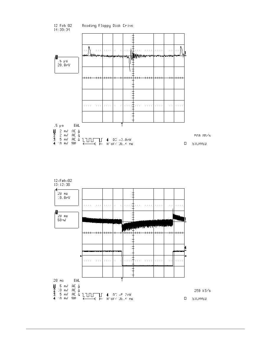
Figure 16. V
tt
with a Transient Load I
Vdd
= 0 to 8.0 A, I
Vtt
= 1.25 A Sourcing and V
REF
= 2.45 mA
Channel 1: V
tt
ripple voltage
Channel 2: Transient current load I
Vdd
= 0 to 8.0 A
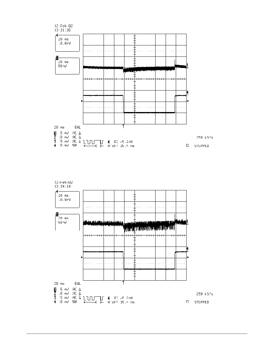
Figure 17. V
REF
with a Transient Load I
Vdd
= 0 to 8.0 A, I
Vtt
= 1.25 A Sourcing and V
REF
= 2.45 mA
Channel 1: V
REF
ripple voltage
Channel 2: Transient current load I
Vdd
= 0 to 8.0 A
AND8079/D
http://onsemi.com
11
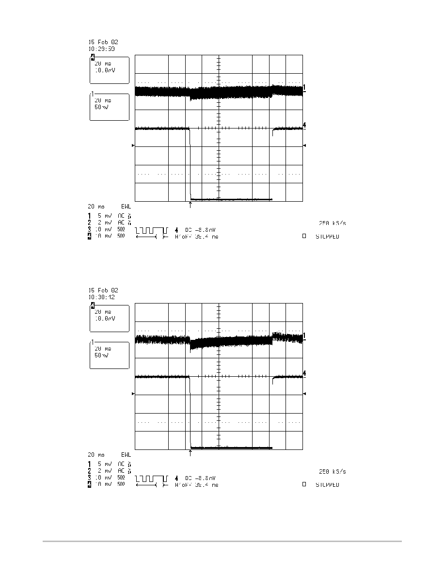
Figure 18. V
dd
with a Transient Load I
Vtt
= -2.0 to +2.0 A, I
Vdd
= 8.0 A and V
REF
= 2.45 mA
Channel 1: V
dd
ripple voltage
Channel 2: Transient current load I
Vtt
= 0 to 4.0 A sourcing
(i.e. ≠2.0 A sinking to +2.0 A sourcing transient current load)
Figure 19. V
tt
with a Transient Load I
Vtt
= -2.0 to +2.0 A, I
Vdd
= 8.0 A and V
REF
= 2.45 mA
Channel 1: V
tt
ripple voltage
Channel 2: Transient current load I
Vtt
= 0 to 4.0 A sourcing
(i.e. ≠2.0 A sinking to +2.0 A sourcing transient current load)
AND8079/D
http://onsemi.com
12
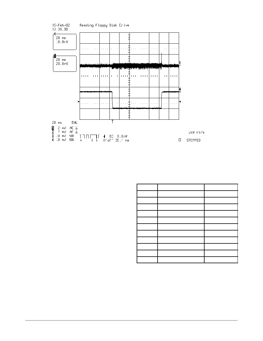
Figure 20. Switching Noise Reflected to the 5.0 V Input Power Supply with a Transient Load I
Vdd
= 0 to 8.0 A,
I
Vtt
= 0 to 4.0 A Sourcing (i.e. ≠2.0 A Sinking to +2.0 A Sourcing Transient Current Load) and V
REF
= 2.45 mA
Channel 1: 5.0 V Input Voltage
Channel 2: Transient current load of I
Vdd
= 0 to 8.0 A
Table 1: Component temperature measured in still air at an
ambient temperature of 23
_C. The load conditions were:
1. V
dd
Transient current load I
Vdd
= 0 to 8.0 A
2. V
tt
Transient current load I
Vtt
= 0 to 4.0 A
sourcing (i.e. ≠2.0 A sinking to +2.0 A sourcing
transient current load)
3. Steady state V
REF
current load I
REF
= 2.5 mA
Table 1.
Circuit
Component
Temperature (
5
C)
V
dd
FET Diode (Q
1
)
41.6
V
dd
Top FET (Q
2
)
54.2
V
dd
Bottom FET (Q
3
)
56.4
V
dd
Input Inductor (L
1
)
42.1
V
dd
Output Inductor (L
2
)
57.9
V
dd
Input Capacitor (C
2
)
33.0
V
dd
Output Capacitor (C
10
)
31.2
V
dd
NCP1571 (U
1
)
55.0
V
tt
LM358 (U
2
)
46.2
V
tt
Top FET (Q
4
)
42.1
V
tt
Bottom FET (Q
5
)
49.3
AND8079/D
http://onsemi.com
13
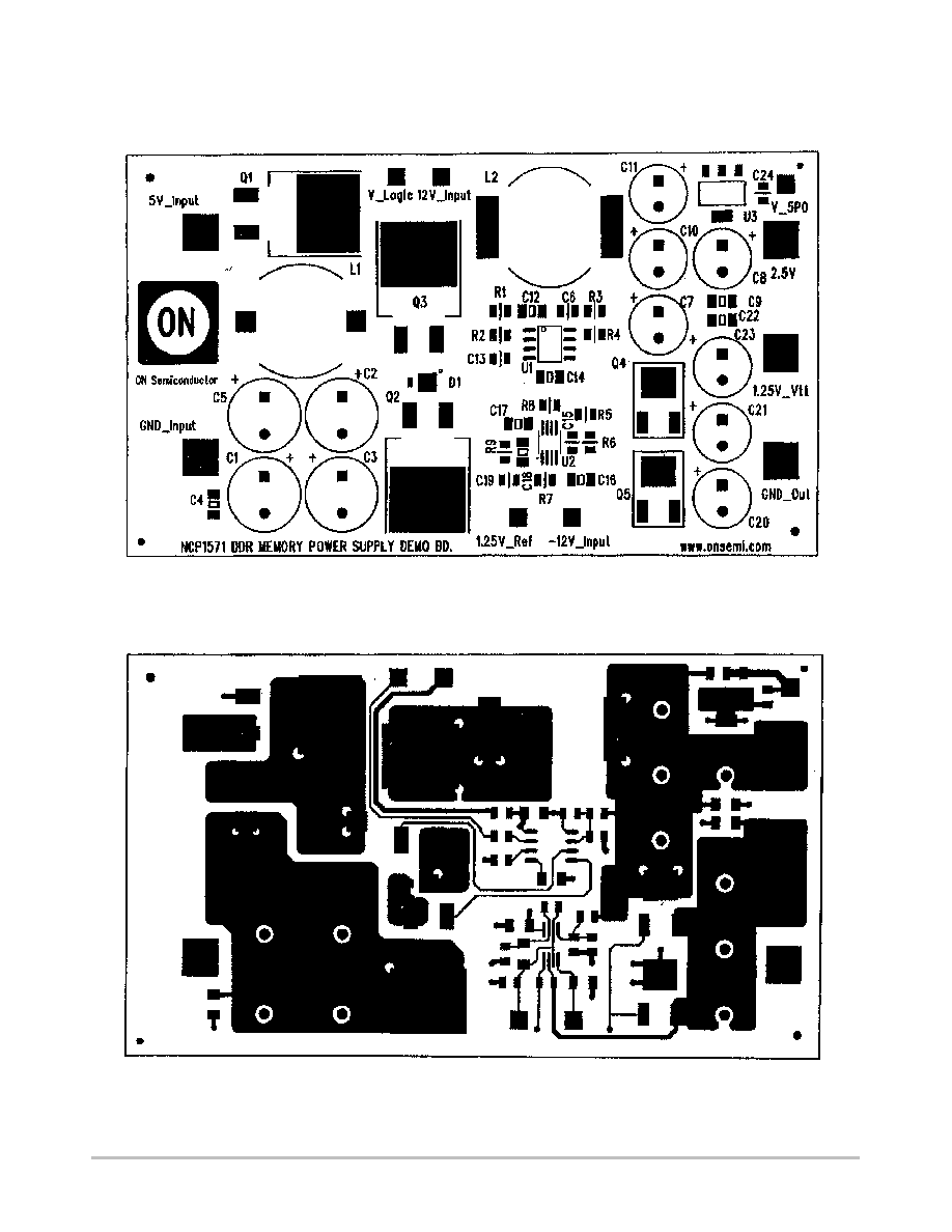
DEMONSTRATION DESIGN PCB
Figure 21. Component Layout
Figure 22. TopSide of PCB (layer 1)
AND8079/D
http://onsemi.com
14
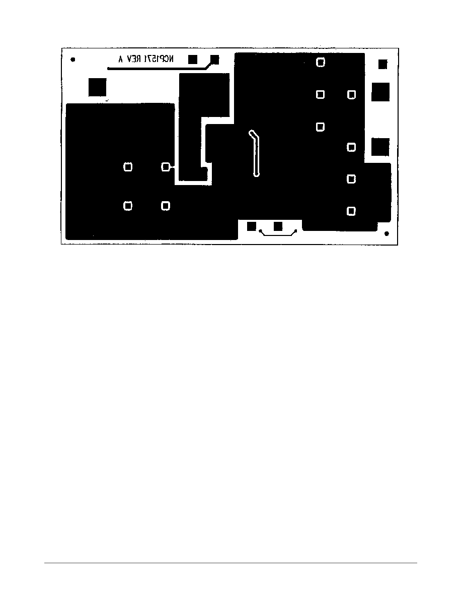
Figure 23. Bottom Side of PCB (layer 2)
AND8079/D
http://onsemi.com
15
0
0.125
0.125
0
2.15
3.80
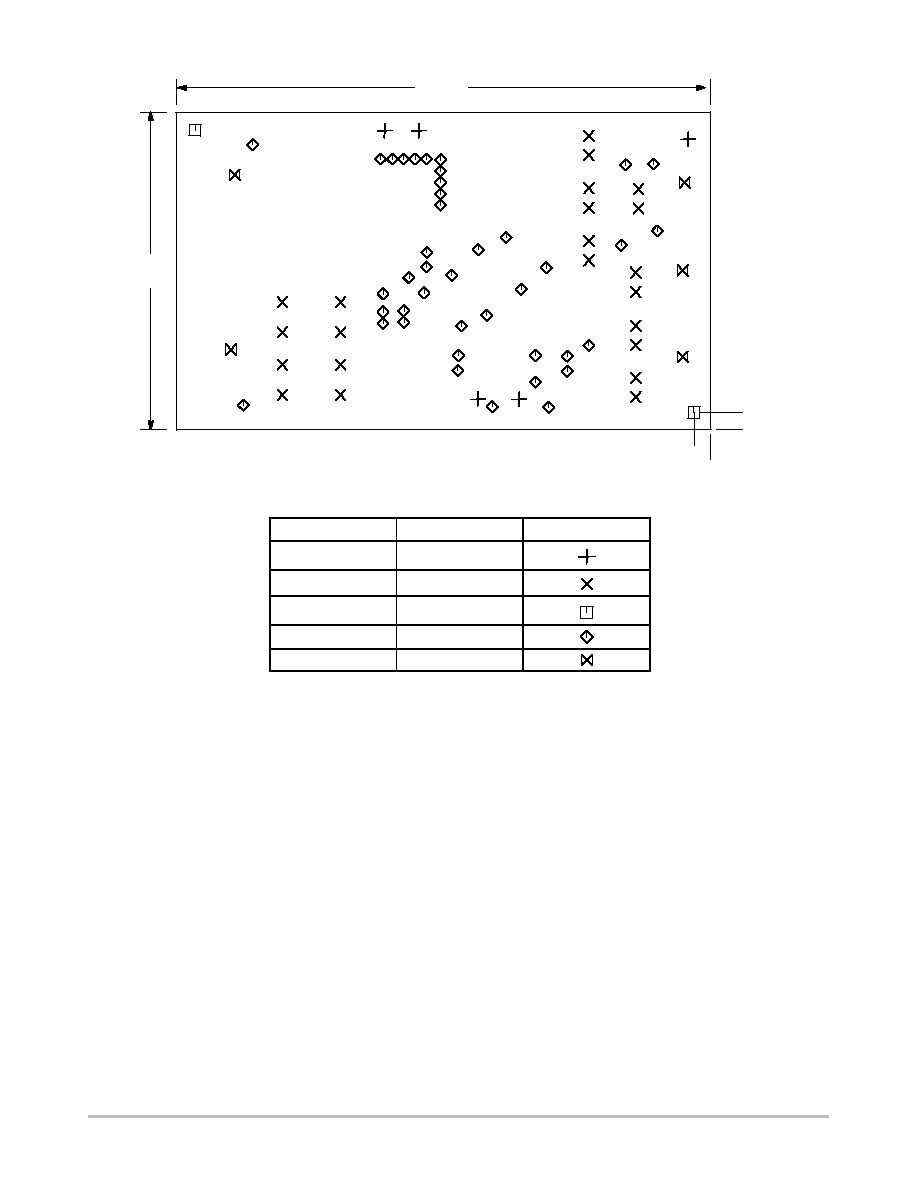
Figure 24. Drill Plot
Size
Qty.
Symbol
62
5
38
22
62
2
18
41
125
5

AND8079/D
http://onsemi.com
16
Table 2. Demonstration Board Bill of Materials
Item
Quantity
Reference
Part
Part No.
Package
Mfg.
Comments
1
4
C1, C2, C3,
C5
1800
m
F, 10 V
MBZ Series
see data sheet
Rubycon
C5 is provisional
2
7
C7, C8, C10,
C11, C20,
C21, C23
1800
m
F, 6.3 V
MBZ Series
see data sheet
Rubycon
C7, C20 and C21
are provisional
3
7
C4, C9, C12,
C14, C16,
C17, C22
0.1
m
F
-
SMT 1206
-
-
4
1
C6
100 pF
-
SMT O805
-
-
5
1
C18
0.15
m
F
-
SMT 1206
-
-
6
1
C13
0.01
m
F
-
SMT O805
-
-
7
1
C15
1.0
m
F
-
SMT O805
-
-
8
1
C19
2.0
m
F
-
SMT O805
-
-
9
1
L1
1.0
m
H
DO3316P-102HC
see data sheet
Coilcraft
-
10
1
L2
2.2
m
H
DO5022P-222HC
see data sheet
Coilcraft
-
11
3
Q1, Q2, Q3
N-Channel
Mosfet
MTB1306
D2PAK
ON
Semiconductor
-
12
1
Q4
N-Channel
Mosfet
NTD4302
DPAK Bent
Lead
ON
Semiconductor
-
13
1
Q5
P-Channel
Mosfet
MTD20P03HDL
DPAK Bent
Lead
ON
Semiconductor
-
14
1
R1
10 ohm
-
SMT O805
-
-
15
1
R2
47 Kohm
-
SMT O805
-
-
16
1
R3
20 Kohm
-
SMT O805
-
-
17
1
R4
13 Kohm
-
SMT O805
-
-
18
2
R5, R6
10 Kohm
-
SMT O805
-
-
19
1
R7
1.0 Kohm
-
SMT O805
-
-
20
1
R8
200 ohm
-
SMT O805
-
-
21
1
R9
100 ohm
-
SMT O805
-
-
22
1
U1
Sync. Buck
Controller
NCP1571
SO-8
ON
Semiconductor
-
23
1
U2
Op-Amp
LM358DMR2
Micro-8
ON
Semiconductor
-
24
1
U3
LDO
Regulator
MC33375ST-2.5T3
SOT-223
ON
Semiconductor
U3 is provisional
25
1
D1
Schottky
Diode
MBRM110LT
PowerMite
ON
Semiconductor
D1 is provisional
NOTE:
The provisional components were not used in the verification of the reference design.
Acknowledgement
The author would like to acknowledge Tod Schiff's
assistance in designing the linear V
dd
circuit.

AND8079/D
http://onsemi.com
17
Notes

AND8079/D
http://onsemi.com
18
Notes

AND8079/D
http://onsemi.com
19
Notes

AND8079/D
http://onsemi.com
20
ON Semiconductor and are registered trademarks of Semiconductor Components Industries, LLC (SCILLC). SCILLC reserves the right to make
changes without further notice to any products herein. SCILLC makes no warranty, representation or guarantee regarding the suitability of its products for any
particular purpose, nor does SCILLC assume any liability arising out of the application or use of any product or circuit, and specifically disclaims any and all
liability, including without limitation special, consequential or incidental damages. "Typical" parameters which may be provided in SCILLC data sheets and/or
specifications can and do vary in different applications and actual performance may vary over time. All operating parameters, including "Typicals" must be
validated for each customer application by customer's technical experts. SCILLC does not convey any license under its patent rights nor the rights of others.
SCILLC products are not designed, intended, or authorized for use as components in systems intended for surgical implant into the body, or other applications
intended to support or sustain life, or for any other application in which the failure of the SCILLC product could create a situation where personal injury or death
may occur. Should Buyer purchase or use SCILLC products for any such unintended or unauthorized application, Buyer shall indemnify and hold SCILLC
and its officers, employees, subsidiaries, affiliates, and distributors harmless against all claims, costs, damages, and expenses, and reasonable attorney fees
arising out of, directly or indirectly, any claim of personal injury or death associated with such unintended or unauthorized use, even if such claim alleges that
SCILLC was negligent regarding the design or manufacture of the part. SCILLC is an Equal Opportunity/Affirmative Action Employer.
PUBLICATION ORDERING INFORMATION
JAPAN: ON Semiconductor, Japan Customer Focus Center
2-9-1 Kamimeguro, Meguro-ku, Tokyo, Japan 153-0051
Phone: 81-3-5773-3850
Email: r14525@onsemi.com
ON Semiconductor Website: http://onsemi.com
For additional information, please contact your local
Sales Representative.
AND8079/D
Literature Fulfillment:
Literature Distribution Center for ON Semiconductor
P.O. Box 5163, Denver, Colorado 80217 USA
Phone: 303-675-2175 or 800-344-3860 Toll Free USA/Canada
Fax: 303-675-2176 or 800-344-3867 Toll Free USA/Canada
Email: ONlit@hibbertco.com
N. American Technical Support: 800-282-9855 Toll Free USA/Canada