 | –≠–ª–µ–∫—Ç—Ä–æ–Ω–Ω—ã–π –∫–æ–º–ø–æ–Ω–µ–Ω—Ç: BAS21LT1 | –°–∫–∞—á–∞—Ç—å:  PDF PDF  ZIP ZIP |

©
Semiconductor Components Industries, LLC, 2005
April, 2005 - Rev. 7
1
Publication Order Number:
BAS19LT1/D
BAS19LT1, BAS20LT1,
BAS21LT1, BAS21DW5T1
Preferred Devices
High Voltage
Switching Diode
Device Marking:
∑
BAS19LT1 = JP
∑
BAS20LT1 = JR
∑
BAS21LT1 = JS
∑
BAS21DW5T1 = JS
Features
∑
Pb-Free Packages are Available
MAXIMUM RATINGS
Rating
Symbol
Value
Unit
Continuous Reverse Voltage
BAS19
BAS20
BAS21
V
R
120
200
250
Vdc
Repetitive Peak Reverse Voltage
BAS19
BAS20
BAS21
V
RRM
120
200
250
Vdc
Continuous Forward Current
I
F
200
mAdc
Peak Forward Surge Current
I
FM(surge)
625
mAdc
Maximum Junction Temperature
T
Jmax
150
∞
C
Power Dissipation (Note 4)
P
D
385
mW
Maximum ratings are those values beyond which device damage can occur.
Maximum ratings applied to the device are individual stress limit values (not
normal operating conditions) and are not valid simultaneously. If these limits are
exceeded, device functional operation is not implied, damage may occur and
reliability may be affected.
1. Mounted on FR-5 Board = 1.0 x 0.75 x 0.062 in.
HIGH VOLTAGE
SWITCHING DIODE
Preferred devices are recommended choices for future use
and best overall value.
5
CATHODE
1
ANODE
Jx M
MARKING DIAGRAMS
Jx = Specific Device Code
x = P, R or S
M = Date Code
http://onsemi.com
3
CATHODE
1
ANODE
4
CATHODE
3
ANODE
XX
d
XX = Specific Device Code
d
= Date Code
SOT-23 (TO-236)
CASE 318
STYLE 8
SC-88A (SOT-353)
CASE 419A
SOT-23
SC-88A
ORDERING INFORMATION
See detailed ordering and shipping information in the package
dimensions section on page 4 of this data sheet.

BAS19LT1, BAS20LT1, BAS21LT1, BAS21DW5T1
http://onsemi.com
2
THERMAL CHARACTERISTICS (SOT-23)
Characteristic
Symbol
Max
Unit
Total Device Dissipation FR-5 Board
(Note 2)
T
A
= 25
∞
C
Derate above 25
∞
C
P
D
225
1.8
mW
mW/
∞
C
Thermal Resistance
Junction-to-Ambient (SOT-23)
R
q
JA
556
∞
C/W
Total Device Dissipation Alumina Substrate
(Note 3)
T
A
= 25
∞
C
Derate above 25
∞
C
P
D
300
2.4
mW
mW/
∞
C
Thermal Resistance Junction-to-Ambient
R
q
JA
417
∞
C/W
Junction and Storage
Temperature Range
T
J
, T
stg
-55 to +150
∞
C
THERMAL CHARACTERISTICS (SC-88A)
Characteristic
Symbol
Max
Unit
Power Dissipation (Note 4)
P
D
385
mW
Thermal Resistance -
Junction-to-Ambient
Derate Above 25
∞
C
R
q
JA
328
3.0
∞
C/W
mW/
∞
C
Maximum Junction Temperature
T
Jmax
150
∞
C
Operating Junction and Storage Temperature Range
T
J
, T
stg
-55 to +150
∞
C
2. FR-5 = 1.0
0.75
0.062 in.
3. Alumina = 0.4
0.3
0.024 in. 99.5% alumina.
4. Mounted on FR-5 Board = 1.0 x 0.75 x 0.062 in.
ELECTRICAL CHARACTERISTICS
(T
A
= 25
∞
C unless otherwise noted)
Characteristic
Symbol
Min
Max
Unit
Reverse Voltage Leakage Current
(V
R
= 100 Vdc)
BAS19
(V
R
= 150 Vdc)
BAS20
(V
R
= 200 Vdc)
BAS21
(V
R
= 100 Vdc, T
J
= 150
∞
C)
BAS19
(V
R
= 150 Vdc, T
J
= 150
∞
C)
BAS20
(V
R
= 200 Vdc, T
J
= 150
∞
C)
BAS21
I
R
-
-
-
-
-
-
0.1
0.1
0.1
100
100
100
m
Adc
Reverse Breakdown Voltage
(I
BR
= 100
m
Adc)
BAS19
(I
BR
= 100
m
Adc)
BAS20
(I
BR
= 100
m
Adc)
BAS21
V
(BR)
120
200
250
-
-
-
Vdc
Forward Voltage
(I
F
= 100 mAdc)
(I
F
= 200 mAdc)
V
F
-
-
1.0
1.25
Vdc
Diode Capacitance (V
R
= 0, f = 1.0 MHz)
C
D
-
5.0
pF
Reverse Recovery Time (I
F
= I
R
= 30 mAdc, I
R(REC)
= 3.0 mAdc, R
L
= 100)
t
rr
-
50
ns

BAS19LT1, BAS20LT1, BAS21LT1, BAS21DW5T1
http://onsemi.com
3
Notes: 1. A 2.0 k
W
variable resistor adjusted for a Forward Current (I
F
) of 30 mA.
Notes:
2. Input pulse is adjusted so I
R(peak)
is equal to 30 mA.
Notes:
3. t
p
ª t
rr
+10 V
2.0 k
820 W
0.1 mF
D.U.T.
V
R
100 mH
0.1 mF
50 W OUTPUT
PULSE
GENERATOR
50 W INPUT
SAMPLING
OSCILLOSCOPE
t
r
t
p
t
10%
90%
I
F
I
R
t
rr
t
I
R(REC)
= 3.0 mA
OUTPUT PULSE
(I
F
= I
R
= 30 mA; MEASURED
at I
R(REC)
= 3.0 mA)
I
F
INPUT SIGNAL
Figure 1. Recovery Time Equivalent Test Circuit
Figure 2. Forward Voltage
Figure 3. Reverse Leakage
7000
REVERSE VOLTAGE (V)
5000
3000
5
0
2
1
6000
4000
6
5
10
20
50
100
200
1
2
3
4
300
T
A
= 155
∞
C
T
A
= 25
∞
C
T
A
= -55
∞
C
REVERSE CURRENT (nA)
FORWARD CURRENT (mA)
T
A
= -55
∞
C
1
10
100
1000
1
200
400
600
800
1000
1200
FOR
W
ARD VOL
T
AGE (mV)
155
∞
C
25
∞
C

BAS19LT1, BAS20LT1, BAS21LT1, BAS21DW5T1
http://onsemi.com
4
ORDERING INFORMATION
Device
Package
Shipping
BAS19LT1
SOT-23
3000 T
/R
l
BAS19LT1G
SOT-23
(Pb-Free)
3000 Tape/Reel
BAS19LT3
SOT-23
10000 T
/R
l
BAS19LT3G
SOT-23
(Pb-Free)
10000 Tape/Reel
BAS20LT1
SOT-23
3000 T
/R
l
BAS20LT1G
SOT-23
(Pb-Free)
3000 Tape/Reel
BAS21LT1
SOT-23
3000 T
/R
l
BAS21LT1G
SOT-23
(Pb-Free)
3000 Tape/Reel
BAS21LT3
SOT-23
10000 T
/R
l
BAS21LT3G
SOT-23
(Pb-Free)
10000 Tape/Reel
BAS21DW5T1
SC-88A
3000 T
/R
l
BAS21DW5T1G
SC-88A
(Pb-Free)
3000 Tape/Reel
For information on tape and reel specifications, including part orientation and tape sizes, please refer to our Tape and Reel Packaging
Specifications Brochure, BRD8011/D.
BAS19LT1, BAS20LT1, BAS21LT1, BAS21DW5T1
http://onsemi.com
5
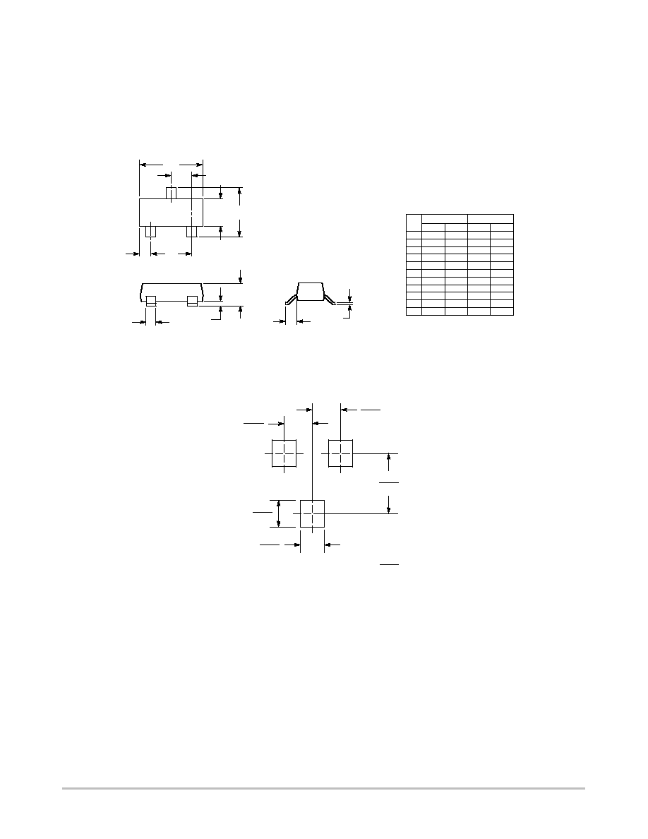
PACKAGE DIMENSIONS
SOT-23 (TO-236)
CASE 318-09
ISSUE AH
DIM
A
MIN
MAX
MIN
MAX
MILLIMETERS
0.1102 0.1197
2.80
3.04
INCHES
B 0.0472 0.0551
1.20
1.40
C 0.0385 0.0498
0.99
1.26
D 0.0140 0.0200
0.36
0.50
G 0.0670 0.0826
1.70
2.10
H 0.0040 0.0098
0.10
0.25
J 0.0034 0.0070
0.085
0.177
K 0.0180 0.0236
0.45
0.60
L 0.0350 0.0401
0.89
1.02
S 0.0830 0.0984
2.10
2.50
V 0.0177 0.0236
0.45
0.60
NOTES:
1. DIMENSIONING AND TOLERANCING PER ANSI
Y14.5M, 1982.
2. CONTROLLING DIMENSION: INCH.
3. MAXIUMUM LEAD THICKNESS INCLUDES LEAD
FINISH THICKNESS. MINIMUM LEAD THICKNESS
IS THE MINIMUM THICKNESS OF BASE
MATERIAL.
4. 318-01, -02, AND -06 OBSOLETE, NEW
STANDARD 318-09.
1
3
2
A
L
B
S
V
G
D
H
C
K
J
STYLE 8:
PIN 1. ANODE
2. NO CONNECTION
3. CATHODE
mm
inches
SCALE 10:1
0.8
0.031
0.9
0.035
0.95
0.037
0.95
0.037
2.0
0.079
*For additional information on our Pb-Free strategy and soldering
details, please download the ON Semiconductor Soldering and
Mounting Techniques Reference Manual, SOLDERRM/D.
SOLDERING FOOTPRINT*
BAS19LT1, BAS20LT1, BAS21LT1, BAS21DW5T1
http://onsemi.com
6
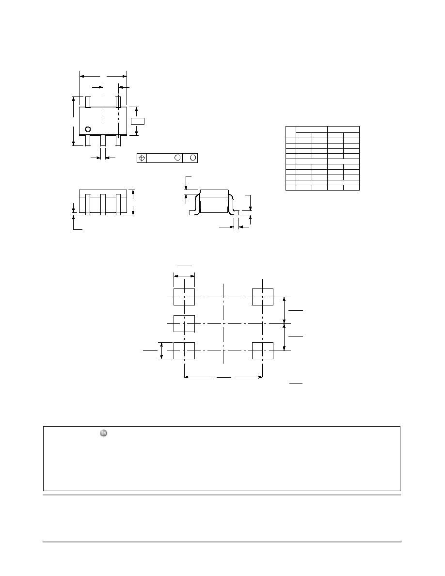
PACKAGE DIMENSIONS
NOTES:
1. DIMENSIONING AND TOLERANCING
PER ANSI Y14.5M, 1982.
2. CONTROLLING DIMENSION: INCH.
3. 419A-01 OBSOLETE. NEW STANDARD
419A-02.
4. DIMENSIONS A AND B DO NOT INCLUDE
MOLD FLASH, PROTRUSIONS, OR GATE
BURRS.
DIM
A
MIN
MAX
MIN
MAX
MILLIMETERS
1.80
2.20
0.071
0.087
INCHES
B
1.15
1.35
0.045
0.053
C
0.80
1.10
0.031
0.043
D
0.10
0.30
0.004
0.012
G
0.65 BSC
0.026 BSC
H
---
0.10
---
0.004
J
0.10
0.25
0.004
0.010
K
0.10
0.30
0.004
0.012
N
0.20 REF
0.008 REF
S
2.00
2.20
0.079
0.087
B
0.2 (0.008)
M
M
1
2
3
4
5
A
G
S
D
5 PL
H
C
N
J
K
-B-
SC-88A (SOT-353)
CASE 419A-02
ISSUE G
mm
inches
SCALE 20:1
0.65
0.025
0.65
0.025
0.50
0.0197
0.40
0.0157
1.9
0.0748
*For additional information on our Pb-Free strategy and soldering
details, please download the ON Semiconductor Soldering and
Mounting Techniques Reference Manual, SOLDERRM/D.
SOLDERING FOOTPRINT*
ON Semiconductor and are registered trademarks of Semiconductor Components Industries, LLC (SCILLC). SCILLC reserves the right to make changes without further notice
to any products herein. SCILLC makes no warranty, representation or guarantee regarding the suitability of its products for any particular purpose, nor does SCILLC assume any liability
arising out of the application or use of any product or circuit, and specifically disclaims any and all liability, including without limitation special, consequential or incidental damages.
"Typical" parameters which may be provided in SCILLC data sheets and/or specifications can and do vary in different applications and actual performance may vary over time. All
operating parameters, including "Typicals" must be validated for each customer application by customer's technical experts. SCILLC does not convey any license under its patent rights
nor the rights of others. SCILLC products are not designed, intended, or authorized for use as components in systems intended for surgical implant into the body, or other applications
intended to support or sustain life, or for any other application in which the failure of the SCILLC product could create a situation where personal injury or death may occur. Should
Buyer purchase or use SCILLC products for any such unintended or unauthorized application, Buyer shall indemnify and hold SCILLC and its officers, employees, subsidiaries, affiliates,
and distributors harmless against all claims, costs, damages, and expenses, and reasonable attorney fees arising out of, directly or indirectly, any claim of personal injury or death
associated with such unintended or unauthorized use, even if such claim alleges that SCILLC was negligent regarding the design or manufacture of the part. SCILLC is an Equal
Opportunity/Affirmative Action Employer. This literature is subject to all applicable copyright laws and is not for resale in any manner.
PUBLICATION ORDERING INFORMATION
N. American Technical Support: 800-282-9855 Toll Free
USA/Canada
Japan: ON Semiconductor, Japan Customer Focus Center
2-9-1 Kamimeguro, Meguro-ku, Tokyo, Japan 153-0051
Phone: 81-3-5773-3850
BAS19LT1/D
LITERATURE FULFILLMENT:
Literature Distribution Center for ON Semiconductor
P.O. Box 61312, Phoenix, Arizona 85082-1312 USA
Phone: 480-829-7710 or 800-344-3860 Toll Free USA/Canada
Fax: 480-829-7709 or 800-344-3867 Toll Free USA/Canada
Email: orderlit@onsemi.com
ON Semiconductor Website: http://onsemi.com
Order Literature: http://www.onsemi.com/litorder
For additional information, please contact your
local Sales Representative.