©
Semiconductor Components Industries, LLC, 2004
June, 2004 - Rev. 6
1
Publication Order Number:
BC846ALT1/D
BC846ALT1 Series
BC846, BC847 and BC848 are Preferred Devices
General Purpose
Transistors
NPN Silicon
Features
∑
Pb-Free Packages are Available
∑
Moisture Sensitivity Level: 1
∑
ESD Rating - Human Body Model: >4000 V
ESD Rating
- Machine Model: >400 V
MAXIMUM RATINGS
Rating
Symbol
Value
Unit
Collector-Emitter Voltage
BC846
BC847, BC850
BC848, BC849
V
CEO
65
45
30
Vdc
Collector-Base Voltage
BC846
BC847, BC850
BC848, BC849
V
CBO
80
50
30
Vdc
Emitter-Base Voltage
BC846
BC847, BC850
BC848, BC849
V
EBO
6.0
6.0
5.0
Vdc
Collector Current - Continuous
I
C
100
mAdc
Maximum ratings are those values beyond which device damage can occur.
Maximum ratings applied to the device are individual stress limit values (not
normal operating conditions) and are not valid simultaneously. If these limits
are exceeded, device functional operation is not implied, damage may occur
and reliability may be affected.
THERMAL CHARACTERISTICS
Characteristic
Symbol
Max
Unit
Total Device Dissipation FR- 5 Board,
(Note 1)
T
A
= 25
∞
C
Derate above 25
∞
C
P
D
225
1.8
mW
mW/
∞
C
Thermal Resistance,
Junction-to-Ambient (Note 1)
R
q
JA
556
∞
C/W
Total Device Dissipation
Alumina Substrate (Note 2)
T
A
= 25
∞
C
Derate above 25
∞
C
P
D
300
2.4
mW
mW/
∞
C
Thermal Resistance,
Junction-to-Ambient (Note 2)
R
q
JA
417
∞
C/W
Junction and Storage
Temperature Range
T
J
, T
stg
- 55 to
+150
∞
C
1. FR- 5 = 1.0
0.75
0.062 in.
2. Alumina = 0.4
0.3
0.024 in 99.5% alumina.
SOT-23
CASE 318
STYLE 6
MARKING DIAGRAM
xxD
1
2
3
Preferred devices are recommended choices for future use
and best overall value.
COLLECTOR
3
1
BASE
2
EMITTER
http://onsemi.com
xx
= Specific Device Code
D
= Date Code
See detailed ordering and shipping information in the package
dimensions section on page 5 of this data sheet.
ORDERING INFORMATION

BC846ALT1 Series
http://onsemi.com
2
ELECTRICAL CHARACTERISTICS
(T
A
= 25
∞
C unless otherwise noted)
Characteristic
Symbol
Min
Typ
Max
Unit
OFF CHARACTERISTICS
Collector - Emitter Breakdown Voltage BC846A,B
(I
C
= 10 mA)
BC847A,B,C, BC850B,C
BC848A,B,C, BC849B,C
V
(BR)CEO
65
45
30
-
-
-
-
-
-
V
Collector - Emitter Breakdown Voltage BC846A,B
(I
C
= 10
m
A, V
EB
= 0)
BC847A,B,C BC850B,C
BC848A,B,C, BC849B,C
V
(BR)CES
80
50
30
-
-
-
-
-
-
V
Collector - Base Breakdown Voltage
BC846A,B
(I
C
= 10
m
A)
BC847A,B,C, BC850B,C
BC848A,B,C, BC849B,C
V
(BR)CBO
80
50
30
-
-
-
-
-
-
V
Emitter - Base Breakdown Voltage
BC846A,B
(I
E
= 1.0
m
A)
BC847A,B,C, BC850B,C
BC848A,B,C, BC849B,C
V
(BR)EBO
6.0
6.0
5.0
-
-
-
-
-
-
V
Collector Cutoff Current (V
CB
= 30 V)
(V
CB
= 30 V, T
A
= 150
∞
C)
I
CBO
-
-
-
-
15
5.0
nA
m
A
ON CHARACTERISTICS
DC Current Gain
BC846A, BC847A, BC848A
(I
C
= 10
m
A, V
CE
= 5.0 V)
BC846B, BC847B, BC848B
BC847C, BC848C
(I
C
= 2.0 mA, V
CE
= 5.0 V)
BC846A, BC847A, BC848A
BC846B, BC847B, BC848B,
BC849B, BC850B
BC847C, BC848C, BC849C, BC850C
h
FE
-
-
-
110
200
420
90
150
270
180
290
520
-
-
-
220
450
800
-
Collector - Emitter Saturation Voltage (I
C
= 10 mA, I
B
= 0.5 mA)
Collector - Emitter Saturation Voltage
(I
C
= 100 mA, I
B
= 5.0 mA)
V
CE(sat)
-
-
-
-
0.25
0.6
V
Base - Emitter Saturation Voltage (I
C
= 10 mA, I
B
= 0.5 mA)
Base - Emitter Saturation Voltage
(I
C
= 100 mA, I
B
= 5.0 mA)
V
BE(sat)
-
-
0.7
0.9
-
-
V
Base - Emitter Voltage (I
C
= 2.0 mA, V
CE
= 5.0 V)
Base - Emitter Voltage
(I
C
= 10 mA, V
CE
= 5.0 V)
V
BE(on)
580
-
660
-
700
770
mV
SMALL-SIGNAL CHARACTERISTICS
Current - Gain - Bandwidth Product
(I
C
= 10 mA, V
CE
= 5.0 Vdc, f = 100 MHz)
f
T
100
-
-
MHz
Output Capacitance (V
CB
= 10 V, f = 1.0 MHz)
C
obo
-
-
4.5
pF
Noise Figure (I
C
= 0.2 mA,
V
CE
= 5.0 Vdc, R
S
= 2.0 k
W
,
BC846A,B, BC847A,B,C, BC848A,B,C
f = 1.0 kHz, BW = 200 Hz)
BC849B,C, BC850B,C
NF
-
-
-
-
10
4.0
dB
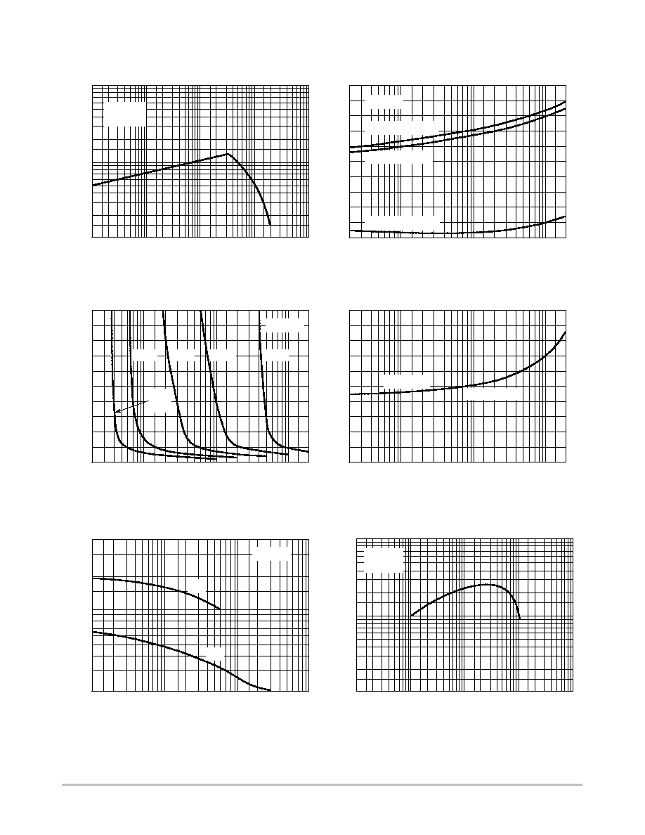
Figure 1.

BC846ALT1 Series
http://onsemi.com
3
BC847, BC848, BC849, BC850
Figure 1. Normalized DC Current Gain
I
C
, COLLECTOR CURRENT (mAdc)
2.0
Figure 2. "Saturation" and "On" Voltages
I
C
, COLLECTOR CURRENT (mAdc)
0.2
0.5
1.0
10
20
50
0.2
100
Figure 3. Collector Saturation Region
I
B
, BASE CURRENT (mA)
Figure 4. Base-Emitter Temperature Coefficient
I
C
, COLLECTOR CURRENT (mA)
2.0
5.0
200
0.6
0.7
0.8
0.9
1.0
0.5
0
0.2
0.4
0.1
0.3
1.6
1.2
2.0
2.8
2.4
1.2
1.6
2.0
0.02
1.0
10
0
20
0.1
0.4
0.8
h FE
, NORMALIZED DC CURRENT
GAIN
V
,
VOL
T
AGE (VOL
TS)
V CE
, COLLECT
OR-EMITTER VOL
T
AGE (V)
VB
,
TEMPERA
TURE COEFFICIENT
(mV/
C)
∞
1.5
1.0
0.8
0.6
0.4
0.3
0.2
0.5
1.0
10
20
50
2.0
100
70
30
7.0
5.0
3.0
0.7
0.3
0.1
0.2
1.0
10
100
T
A
= 25
∞
C
V
BE(sat)
@ I
C
/I
B
= 10
V
CE(sat)
@ I
C
/I
B
= 10
V
BE(on)
@ V
CE
= 10 V
V
CE
= 10 V
T
A
= 25
∞
C
-55
∞
C to +125
∞
C
T
A
= 25
∞
C
I
C
= 50 mA
I
C
= 100 mA
I
C
= 200 mA
I
C
=
20 mA
I
C
=
10 mA
1.0
Figure 5. Capacitances
V
R
, REVERSE VOLTAGE (VOLTS)
10
Figure 6. Current-Gain - Bandwidth Product
I
C
, COLLECTOR CURRENT (mAdc)
0.4 0.6
1.0
10
20
1.0
2.0
6.0
40
80
100
200
300
400
60
20
40
30
7.0
5.0
3.0
2.0
0.7 1.0
10
20
2.0
50
30
7.0
5.0
3.0
0.5
V
CE
= 10 V
T
A
= 25
∞
C
C, CAP
ACIT
ANCE (pF)
f, CURRENT-GAIN - BANDWIDTH PRODUCT
(MHz)
T
0.8
4.0
8.0
T
A
= 25
∞
C
C
ob
C
ib