 | Электронный компонент: BD159 | Скачать:  PDF PDF  ZIP ZIP |
1
Motorola Bipolar Power Transistor Device Data
Plastic Medium Power NPN
Silicon Transistor
. . . designed for power output stages for television, radio, phonograph and other
consumer product applications.
╖
Suitable for Transformerless, Line¡Operated Equipment
╖
Thermopad
{
Construction Provides High Power Dissipation Rating for High
Reliability
╬╬╬╬╬╬╬╬╬╬╬╬╬╬╬╬╬╬╬╬╬╬╬
╬╬╬╬╬╬╬╬╬╬╬╬╬╬╬╬╬╬╬╬╬╬╬
MAXIMUM RATINGS
╬╬╬╬╬╬╬╬╬╬╬╬╬
╬╬╬╬╬╬╬╬╬╬╬╬╬
Rating
╬╬╬╬
╬╬╬╬
Symbol
╬╬╬╬╬╬
╬╬╬╬╬╬
Max
╬╬╬
╬╬╬
Unit
╬╬╬╬╬╬╬╬╬╬╬╬╬
╬╬╬╬╬╬╬╬╬╬╬╬╬
Collector¡Emitter Voltage
╬╬╬╬
╬╬╬╬
VCEO
╬╬╬╬╬╬
╬╬╬╬╬╬
350
╬╬╬
╬╬╬
Vdc
╬╬╬╬╬╬╬╬╬╬╬╬╬
╬╬╬╬╬╬╬╬╬╬╬╬╬
Collector¡Base Voltage
╬╬╬╬
╬╬╬╬
VCB
╬╬╬╬╬╬
╬╬╬╬╬╬
375
╬╬╬
╬╬╬
Vdc
╬╬╬╬╬╬╬╬╬╬╬╬╬
╬╬╬╬╬╬╬╬╬╬╬╬╬
Emitter¡Base Voltage
╬╬╬╬
╬╬╬╬
VEB
╬╬╬╬╬╬
╬╬╬╬╬╬
5.0
╬╬╬
╬╬╬
Vdc
╬╬╬╬╬╬╬╬╬╬╬╬╬
╬
╬╬╬╬╬╬╬╬╬╬╬
╬
╬╬╬╬╬╬╬╬╬╬╬╬╬
Collector Current -- Continuous
Peak
╬╬╬╬
╬
╬╬
╬
╬╬╬╬
IC
╬╬╬╬╬╬
╬
╬╬╬╬
╬
╬╬╬╬╬╬
0.5
1.0
╬╬╬
╬
╬
╬
╬╬╬
Adc
╬╬╬╬╬╬╬╬╬╬╬╬╬
╬╬╬╬╬╬╬╬╬╬╬╬╬
Base Current
╬╬╬╬
╬╬╬╬
IB
╬╬╬╬╬╬
╬╬╬╬╬╬
0.25
╬╬╬
╬╬╬
Adc
╬╬╬╬╬╬╬╬╬╬╬╬╬
╬╬╬╬╬╬╬╬╬╬╬╬╬
Total Device Dissipation @ TC = 25
_
C
Derate above 25
_
C
╬╬╬╬
╬╬╬╬
PD
╬╬╬╬╬╬
╬╬╬╬╬╬
20
0.16
╬╬╬
╬╬╬
Watts
W/
_
C
╬╬╬╬╬╬╬╬╬╬╬╬╬
╬
╬╬╬╬╬╬╬╬╬╬╬
╬
╬╬╬╬╬╬╬╬╬╬╬╬╬
Operating and Storage Junction
Temperature Range
╬╬╬╬
╬
╬╬
╬
╬╬╬╬
TJ, Tstg
╬╬╬╬╬╬
╬
╬╬╬╬
╬
╬╬╬╬╬╬
¡ 65 to + 150
╬╬╬
╬
╬
╬
╬╬╬
_
C
╬╬╬╬╬╬╬╬╬╬╬╬╬╬╬╬╬╬╬╬╬╬╬
╬╬╬╬╬╬╬╬╬╬╬╬╬╬╬╬╬╬╬╬╬╬╬
THERMAL CHARACTERISTICS
╬╬╬╬╬╬╬╬╬╬╬╬
╬╬╬╬╬╬╬╬╬╬╬╬
Characteristic
╬╬╬╬╬
╬╬╬╬╬
Symbol
╬╬╬╬╬╬
╬╬╬╬╬╬
Max
╬╬╬
╬╬╬
Unit
╬╬╬╬╬╬╬╬╬╬╬╬
╬╬╬╬╬╬╬╬╬╬╬╬
Thermal Resistance, Junction to Case
╬╬╬╬╬
╬╬╬╬╬
JC
╬╬╬╬╬╬
╬╬╬╬╬╬
6.25
╬╬╬
╬╬╬
_
C/W
╬╬╬╬╬╬╬╬╬╬╬╬╬╬╬╬╬╬╬╬╬╬╬╬╬╬╬╬╬╬╬╬╬╬
╬
╬╬╬╬╬╬╬╬╬╬╬╬╬╬╬╬╬╬╬╬╬╬╬╬╬╬╬╬╬╬╬╬
╬
ELECTRICAL CHARACTERISTICS
(TC = 25
_
C unless otherwise noted)
╬╬╬╬╬╬╬╬╬╬╬╬╬╬╬╬╬╬╬
╬
╬╬╬╬╬╬╬╬╬╬╬╬╬╬╬╬╬
╬
Characteristic
╬╬╬╬╬
╬
╬╬╬
╬
Symbol
╬╬╬╬╬
╬
╬╬╬
╬
Min
╬╬╬╬╬
╬
╬╬╬
╬
Max
╬╬╬╬
╬
╬╬
╬
Unit
╬╬╬╬╬╬╬╬╬╬╬╬╬╬╬╬╬╬╬╬╬╬╬╬╬╬╬╬╬╬╬╬╬╬
╬╬╬╬╬╬╬╬╬╬╬╬╬╬╬╬╬╬╬╬╬╬╬╬╬╬╬╬╬╬╬╬╬╬
OFF CHARACTERISTICS
╬╬╬╬╬╬╬╬╬╬╬╬╬╬╬╬╬╬╬
╬
╬╬╬╬╬╬╬╬╬╬╬╬╬╬╬╬╬
╬
╬╬╬╬╬╬╬╬╬╬╬╬╬╬╬╬╬╬╬
Collector¡Emitter Sustaining Voltage
(IC = 1.0 mAdc, IB = 0)
╬╬╬╬╬
╬
╬╬╬
╬
╬╬╬╬╬
BVCEO
╬╬╬╬╬
╬
╬╬╬
╬
╬╬╬╬╬
350
╬╬╬╬╬
╬
╬╬╬
╬
╬╬╬╬╬
--
╬╬╬╬
╬
╬╬
╬
╬╬╬╬
Vdc
╬╬╬╬╬╬╬╬╬╬╬╬╬╬╬╬╬╬╬
╬
╬╬╬╬╬╬╬╬╬╬╬╬╬╬╬╬╬
╬
╬╬╬╬╬╬╬╬╬╬╬╬╬╬╬╬╬╬╬
Collector Cutoff Current
(At rated voltage)
╬╬╬╬╬
╬
╬╬╬
╬
╬╬╬╬╬
ICBO
╬╬╬╬╬
╬
╬╬╬
╬
╬╬╬╬╬
--
╬╬╬╬╬
╬
╬╬╬
╬
╬╬╬╬╬
100
╬╬╬╬
╬
╬╬
╬
╬╬╬╬
╡
Adc
╬╬╬╬╬╬╬╬╬╬╬╬╬╬╬╬╬╬╬
╬
╬╬╬╬╬╬╬╬╬╬╬╬╬╬╬╬╬
╬
Emitter Cutoff Current
(VEB = 5.0 Vdc, IC = 0)
╬╬╬╬╬
╬
╬╬╬
╬
IEBO
╬╬╬╬╬
╬
╬╬╬
╬
--
╬╬╬╬╬
╬
╬╬╬
╬
100
╬╬╬╬
╬
╬╬
╬
╡
Adc
╬╬╬╬╬╬╬╬╬╬╬╬╬╬╬╬╬╬╬╬╬╬╬╬╬╬╬╬╬╬╬╬╬╬
╬╬╬╬╬╬╬╬╬╬╬╬╬╬╬╬╬╬╬╬╬╬╬╬╬╬╬╬╬╬╬╬╬╬
ON CHARACTERISTICS
╬╬╬╬╬╬╬╬╬╬╬╬╬╬╬╬╬╬╬
╬
╬╬╬╬╬╬╬╬╬╬╬╬╬╬╬╬╬
╬
╬╬╬╬╬╬╬╬╬╬╬╬╬╬╬╬╬╬╬
DC Current Gain
(IC = 50 mAdc, VCE = 10 Vdc)
╬╬╬╬╬
╬
╬╬╬
╬
╬╬╬╬╬
hFE
╬╬╬╬╬
╬
╬╬╬
╬
╬╬╬╬╬
30
╬╬╬╬╬
╬
╬╬╬
╬
╬╬╬╬╬
240
╬╬╬╬
╬
╬╬
╬
╬╬╬╬
--
MOTOROLA
SEMICONDUCTOR TECHNICAL DATA
Order this document
by BD159/D
⌐
Motorola, Inc. 1998
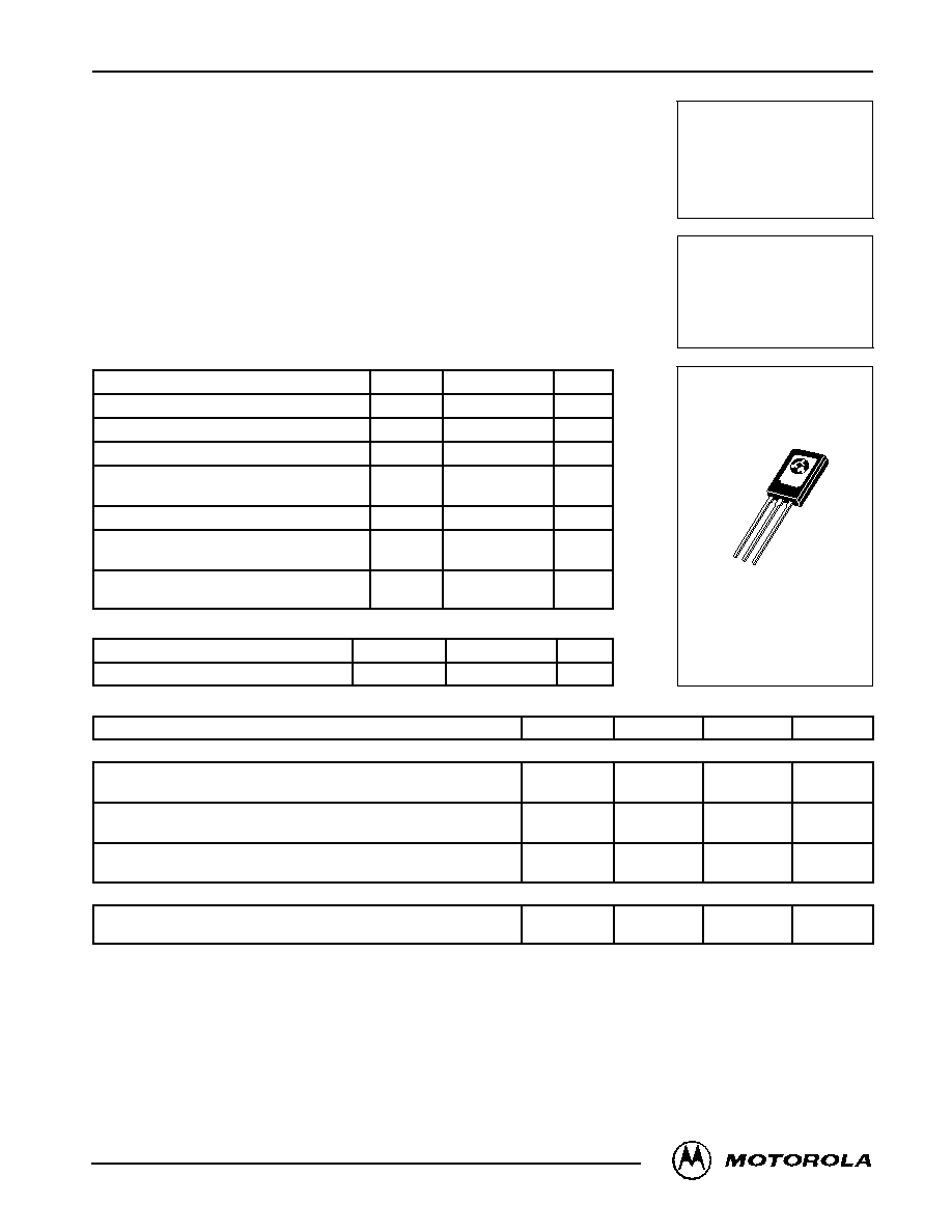
BD159
0.5 AMPERE
POWER TRANSISTOR
NPN SILICON
350 VOLTS
20 WATTS
CASE 77¡09
TO¡225AA TYPE

BD159
2
Motorola Bipolar Power Transistor Device Data
25
20
15
10
5.0
0
20
40
60
80
100
120
140
160
Figure 1. Power¡Temperature Derating Curve
TC, CASE TEMPERATURE (
░
C)
P
D
, POWER DISSIP
A
TION (W
A
TTS)
1.0
10
Figure 2. "On" Voltages
IC, COLLECTOR CURRENT (mA)
0.8
0.6
0.4
0.2
0
20
30
50
100
200 300
500
VBE @ VCE = 10 V
VCE(sat) @ IC/IB = 10
TJ = + 25
░
C
VBE @ IC/IB = 10
IC/IB = 5.0
V
,
VOL
T
AGE
(VOL
TS)
1.0
10
Figure 3. DC Safe Operating Area
VCE, COLLECTOR¡EMITTER VOLTAGE (VOLTS)
0.7
0.5
0.3
0.2
0.1
0.07
0.05
0.01
20
30
50
100
300
200
BONDING WIRE LIMITED
THERMALLY LIMITED @ TC = 25
░
C
(SINGLE PULSE)
SECOND BREAKDOWN LIMITED
0.03
0.02
I C
, COLLECT
OR
CURRENT
(AMPS)
TJ = 150
░
C
dc
500
╡
s
10
╡
s
1.0 ms
The Safe Operating Area Curves indicate IC ¡ VCE limits
below which the device will not enter secondary breakdown.
Collector load lines for specific circuits must fall within the ap-
plicable Safe Area to avoid causing a catastrophic failure. To
insure operation below, the maximum TJ, power¡tempera-
ture derating must be observed for both steady state and
pulse power conditions.
Figure 4. Current Gain
IC, COLLECTOR CURRENT (mAdc)
10
1.0
2.0
3.0
5.0
10
20
30
50
100
200
300
500
300
200
70
30
20
TJ = 150
░
C
h
FE
, DC CURRENT
GAIN
50
100
+ 100
░
C
+ 25
░
C
¡ 55
░
C
7.0
70
VCE = 10 V
VCE = 2.0 V
BD159
3
Motorola Bipolar Power Transistor Device Data
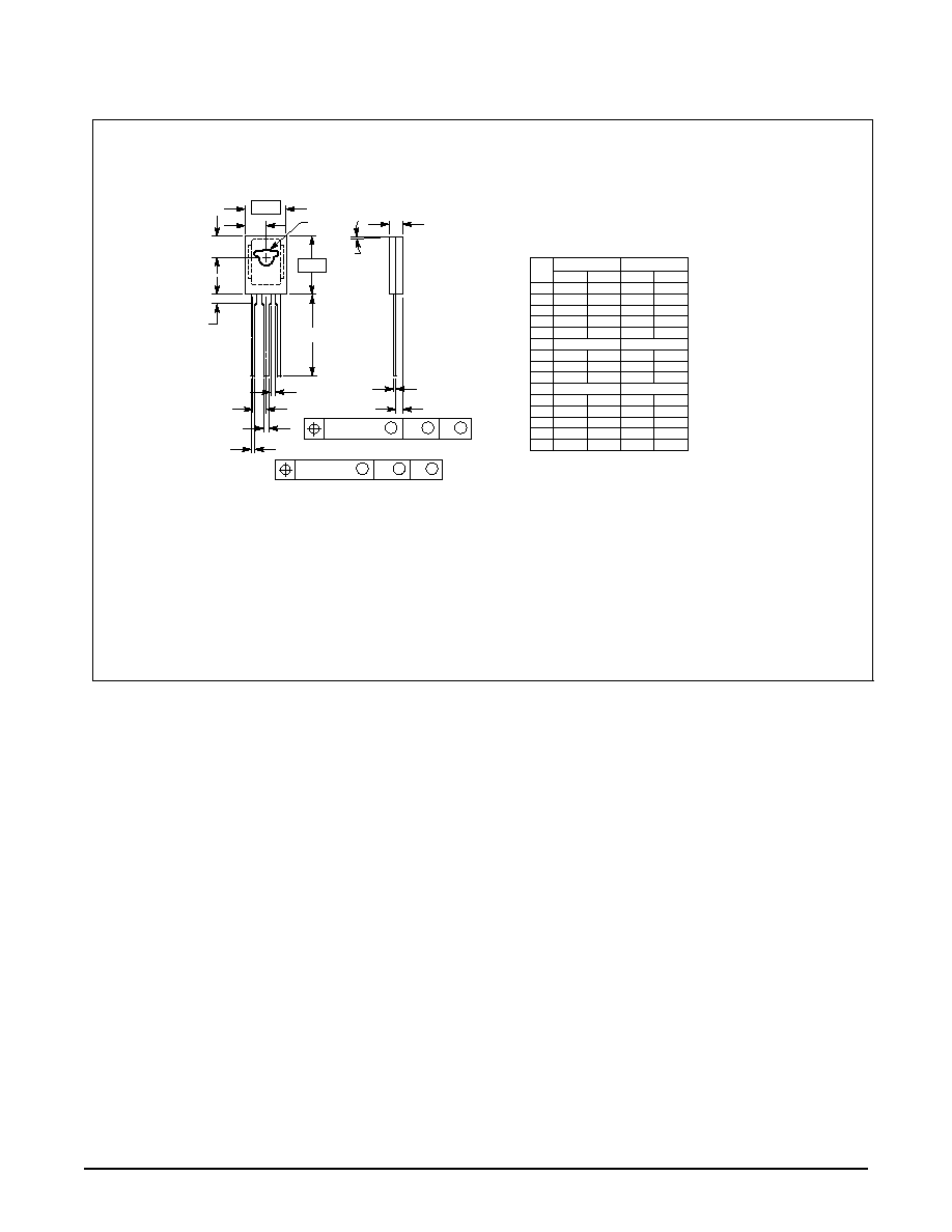
PACKAGE DIMENSIONS
CASE 77¡09
TO¡225AA TYPE
ISSUE W
STYLE 1:
PIN 1.
EMITTER
2.
COLLECTOR
3.
BASE
NOTES:
1. DIMENSIONING AND TOLERANCING PER ANSI
Y14.5M, 1982.
2. CONTROLLING DIMENSION: INCH.
¡B¡
¡A¡
M
K
F
C
Q
H
V
G
S
D
J
R
U
1
3
2
2 PL
M
A
M
0.25 (0.010)
B
M
M
A
M
0.25 (0.010)
B
M
DIM
MIN
MAX
MIN
MAX
MILLIMETERS
INCHES
A
0.425
0.435
10.80
11.04
B
0.295
0.305
7.50
7.74
C
0.095
0.105
2.42
2.66
D
0.020
0.026
0.51
0.66
F
0.115
0.130
2.93
3.30
G
0.094 BSC
2.39 BSC
H
0.050
0.095
1.27
2.41
J
0.015
0.025
0.39
0.63
K
0.575
0.655
14.61
16.63
M
5 TYP
5 TYP
Q
0.148
0.158
3.76
4.01
R
0.045
0.065
1.15
1.65
S
0.025
0.035
0.64
0.88
U
0.145
0.155
3.69
3.93
V
0.040
¡¡¡
1.02
¡¡¡
_
_

BD159
4
Motorola Bipolar Power Transistor Device Data
Motorola reserves the right to make changes without further notice to any products herein. Motorola makes no warranty, representation or guarantee regarding
the suitability of its products for any particular purpose, nor does Motorola assume any liability arising out of the application or use of any product or circuit, and
specifically disclaims any and all liability, including without limitation consequential or incidental damages. "Typical" parameters which may be provided in Motorola
data sheets and/or specifications can and do vary in different applications and actual performance may vary over time. All operating parameters, including "Typicals"
must be validated for each customer application by customer's technical experts. Motorola does not convey any license under its patent rights nor the rights of
others. Motorola products are not designed, intended, or authorized for use as components in systems intended for surgical implant into the body, or other
applications intended to support or sustain life, or for any other application in which the failure of the Motorola product could create a situation where personal injury
or death may occur. Should Buyer purchase or use Motorola products for any such unintended or unauthorized application, Buyer shall indemnify and hold Motorola
and its officers, employees, subsidiaries, affiliates, and distributors harmless against all claims, costs, damages, and expenses, and reasonable attorney fees
arising out of, directly or indirectly, any claim of personal injury or death associated with such unintended or unauthorized use, even if such claim alleges that
Motorola was negligent regarding the design or manufacture of the part. Motorola and are registered trademarks of Motorola, Inc. Motorola, Inc. is an Equal
Opportunity/Affirmative Action Employer.
Mfax is a trademark of Motorola, Inc.
How to reach us:
USA / EUROPE / Locations Not Listed: Motorola Literature Distribution;
JAPAN: Nippon Motorola Ltd.; SPD, Strategic Planning Office, 141,
P.O. Box 5405, Denver, Colorado 80217. 1¡303¡675¡2140 or 1¡800¡441¡2447
4¡32¡1 Nishi¡Gotanda, Shinagawa¡ku, Tokyo, Japan. 81¡3¡5487¡8488
Customer Focus Center: 1¡800¡521¡6274
Mfax
TM
: RMFAX0@email.sps.mot.com ¡ TOUCHTONE 1¡602¡244¡6609
ASIA/PACIFIC: Motorola Semiconductors H.K. Ltd.; 8B Tai Ping Industrial Park,
Motorola Fax Back System
¡ US & Canada ONLY 1¡800¡774¡1848
51 Ting Kok Road, Tai Po, N.T., Hong Kong. 852¡26629298
¡ http://sps.motorola.com/mfax/
HOME PAGE: http://motorola.com/sps/
BD159/D