 | –≠–ª–µ–∫—Ç—Ä–æ–Ω–Ω—ã–π –∫–æ–º–ø–æ–Ω–µ–Ω—Ç: BDW46 | –°–∫–∞—á–∞—Ç—å:  PDF PDF  ZIP ZIP |

©
Semiconductor Components Industries, LLC, 2004
June, 2004 - Rev. 11
Publication Order Number:
BDW42/D
BDW42* - NPN, BDW46,
BDW47* - PNP
Preferred Device
Darlington Complementary
Silicon Power Transistors
This series of plastic, medium-power silicon NPN and PNP
Darlington transistors are designed for general purpose and low speed
switching applications.
Features
∑
Pb-Free Package is Available**
∑
High DC Current Gain - h
FE
= 2500 (typ) @ I
C
= 5.0 Adc.
∑
Collector Emitter Sustaining Voltage @ 30 mAdc:
V
CEO(sus)
= 80 Vdc (min) - BDW46
100 Vdc (min.) - BDW42/BDW47
∑
Low Collector Emitter Saturation Voltage
V
CE(sat)
= 2.0 Vdc (max) @ I
C
= 5.0 Adc
3.0 Vdc (max) @ I
C
= 10.0 Adc
∑
Monolithic Construction with Built-In Base Emitter Shunt resistors
∑
TO-220AB Compact Package
MAXIMUM RATINGS
Rating
Symbol
Value
Unit
Collector-Emitter Voltage
BDW46
BDW42, BDW47
V
CEO
80
100
Vdc
Collector-Base Voltage
BDW46
BDW42, BDW47
V
CB
80
100
Vdc
Emitter-Base Voltage
V
EB
5.0
Vdc
Collector Current
I
C
15
Adc
Base Current
I
B
0.5
Adc
Total Device Dissipation
@ T
C
= 25
∞
C
Derate above 25
∞
C
P
D
85
0.68
W
W/
∞
C
Operating and Storage Junction
Temperature Range
T
J
, T
stg
-55 to
+150
∞
C
Maximum ratings are those values beyond which device damage can occur.
Maximum ratings applied to the device are individual stress limit values (not
normal operating conditions) and are not valid simultaneously. If these limits
are exceeded, device functional operation is not implied, damage may occur
and reliability may be affected.
THERMAL CHARACTERISTICS
Characteristic
Symbol
Max
Unit
Thermal Resistance,
Junction-to-Case
R
q
JC
1.47
∞
C/W
**For additional information on our Pb-Free strategy and soldering details,
please download the ON Semiconductor Soldering and Mounting Techniques
Reference Manual, SOLDERRM/D.
TO-220AB
CASE 221A
STYLE 1
MARKING
DIAGRAM
15 A DARLINGTON
COMPLEMENTARY SILICON
POWER TRANSISTORS
80-100 V, 85 W
http://onsemi.com
1
2
3
4
Device
Package
Shipping
ORDERING INFORMATION
BDW42
TO-220AB
50 Units/Rail
BDW46
TO-220AB
50 Units/Rail
BDW47G
50 Units/Rail
BDW47
TO-220AB
(Pb-Free)
50 Units/Rail
For information on tape and reel specifications,
including part orientation and tape sizes, please
refer to our Tape and Reel Packaging Specifications
Brochure, BRD8011/D.
TO-220AB
*Preferred devices are ON Semiconductor recommended
choices for future use and best overall value
BDWxx
YYWW
xx
= 42, 46 or 47
YY = Year
WW = Work Week
BDW42* - NPN, BDW46, BDW47* - PNP
http://onsemi.com
2
ŒŒŒŒŒŒŒŒŒŒŒŒŒŒŒŒŒŒŒŒŒŒŒŒŒŒŒŒŒŒŒŒŒ
ŒŒŒŒŒŒŒŒŒŒŒŒŒŒŒŒŒŒŒŒŒŒŒŒŒŒŒŒŒŒŒŒŒ
ELECTRICAL CHARACTERISTICS
(T
C
= 25
_
C unless otherwise noted)
ŒŒŒŒŒŒŒŒŒŒŒŒŒŒŒŒŒŒŒŒŒŒ
ŒŒŒŒŒŒŒŒŒŒŒŒŒŒŒŒŒŒŒŒŒŒ
Characteristic
ŒŒŒŒŒ
ŒŒŒŒŒ
Symbol
ŒŒŒ
ŒŒŒ
Min
ŒŒŒŒ
ŒŒŒŒ
Max
ŒŒŒ
ŒŒŒ
Unit
ŒŒŒŒŒŒŒŒŒŒŒŒŒŒŒŒŒŒŒŒŒŒŒŒŒŒŒŒŒŒŒŒŒ
ŒŒŒŒŒŒŒŒŒŒŒŒŒŒŒŒŒŒŒŒŒŒŒŒŒŒŒŒŒŒŒŒŒ
OFF CHARACTERISTICS
ŒŒŒŒŒŒŒŒŒŒŒŒŒŒŒŒŒŒŒŒŒŒ
Œ
ŒŒŒŒŒŒŒŒŒŒŒŒŒŒŒŒŒŒŒŒ
Œ
ŒŒŒŒŒŒŒŒŒŒŒŒŒŒŒŒŒŒŒŒŒŒ
Collector Emitter Sustaining Voltage (Note 1)
(I
C
= 30 mAdc, I
B
= 0)
BDW46
BDW42/BDW47
ŒŒŒŒŒ
Œ
ŒŒŒ
Œ
ŒŒŒŒŒ
V
CEO(sus)
ŒŒŒ
Œ
Œ
Œ
ŒŒŒ
80
100
ŒŒŒŒ
Œ
ŒŒ
Œ
ŒŒŒŒ
-
-
ŒŒŒ
Œ
Œ
Œ
ŒŒŒ
Vdc
ŒŒŒŒŒŒŒŒŒŒŒŒŒŒŒŒŒŒŒŒŒŒ
Œ
ŒŒŒŒŒŒŒŒŒŒŒŒŒŒŒŒŒŒŒŒ
Œ
ŒŒŒŒŒŒŒŒŒŒŒŒŒŒŒŒŒŒŒŒŒŒ
Collector Cutoff Current
(V
CE
= 40 Vdc, I
B
= 0)
BDW46
(V
CE
= 50 Vdc, I
B
= 0)
BDW42/BDW47
ŒŒŒŒŒ
Œ
ŒŒŒ
Œ
ŒŒŒŒŒ
I
CEO
ŒŒŒ
Œ
Œ
Œ
ŒŒŒ
-
-
ŒŒŒŒ
Œ
ŒŒ
Œ
ŒŒŒŒ
2.0
2.0
ŒŒŒ
Œ
Œ
Œ
ŒŒŒ
mAdc
ŒŒŒŒŒŒŒŒŒŒŒŒŒŒŒŒŒŒŒŒŒŒ
Œ
ŒŒŒŒŒŒŒŒŒŒŒŒŒŒŒŒŒŒŒŒ
Œ
ŒŒŒŒŒŒŒŒŒŒŒŒŒŒŒŒŒŒŒŒŒŒ
Collector Cutoff Current
(V
CB
= 80 Vdc, I
E
= 0)
BDW46
(V
CB
= 100 Vdc, I
E
= 0)
BDW42/BDW47
ŒŒŒŒŒ
Œ
ŒŒŒ
Œ
ŒŒŒŒŒ
I
CBO
ŒŒŒ
Œ
Œ
Œ
ŒŒŒ
-
-
ŒŒŒŒ
Œ
ŒŒ
Œ
ŒŒŒŒ
1.0
1.0
ŒŒŒ
Œ
Œ
Œ
ŒŒŒ
mAdc
ŒŒŒŒŒŒŒŒŒŒŒŒŒŒŒŒŒŒŒŒŒŒ
Œ
ŒŒŒŒŒŒŒŒŒŒŒŒŒŒŒŒŒŒŒŒ
Œ
ŒŒŒŒŒŒŒŒŒŒŒŒŒŒŒŒŒŒŒŒŒŒ
Emitter Cutoff Current
(V
BE
= 5.0 Vdc, I
C
= 0)
ŒŒŒŒŒ
Œ
ŒŒŒ
Œ
ŒŒŒŒŒ
I
EBO
ŒŒŒ
Œ
Œ
Œ
ŒŒŒ
-
ŒŒŒŒ
Œ
ŒŒ
Œ
ŒŒŒŒ
2.0
ŒŒŒ
Œ
Œ
Œ
ŒŒŒ
mAdc
ŒŒŒŒŒŒŒŒŒŒŒŒŒŒŒŒŒŒŒŒŒŒŒŒŒŒŒŒŒŒŒŒŒ
ŒŒŒŒŒŒŒŒŒŒŒŒŒŒŒŒŒŒŒŒŒŒŒŒŒŒŒŒŒŒŒŒŒ
ON CHARACTERISTICS (Note 1)
ŒŒŒŒŒŒŒŒŒŒŒŒŒŒŒŒŒŒŒŒŒŒ
Œ
ŒŒŒŒŒŒŒŒŒŒŒŒŒŒŒŒŒŒŒŒ
Œ
ŒŒŒŒŒŒŒŒŒŒŒŒŒŒŒŒŒŒŒŒŒŒ
DC Current Gain
(I
C
= 5.0 Adc, V
CE
= 4.0 Vdc)
(I
C
= 10 Adc, V
CE
= 4.0 Vdc)
ŒŒŒŒŒ
Œ
ŒŒŒ
Œ
ŒŒŒŒŒ
h
FE
ŒŒŒ
Œ
Œ
Œ
ŒŒŒ
1000
250
ŒŒŒŒ
Œ
ŒŒ
Œ
ŒŒŒŒ
-
-
ŒŒŒ
Œ
Œ
Œ
ŒŒŒ
ŒŒŒŒŒŒŒŒŒŒŒŒŒŒŒŒŒŒŒŒŒŒ
Œ
ŒŒŒŒŒŒŒŒŒŒŒŒŒŒŒŒŒŒŒŒ
Œ
ŒŒŒŒŒŒŒŒŒŒŒŒŒŒŒŒŒŒŒŒŒŒ
Collector-Emitter Saturation Voltage
(I
C
= 5.0 Adc, I
B
= 10 mAdc)
(I
C
= 10 Adc, I
B
= 50 mAdc)
ŒŒŒŒŒ
Œ
ŒŒŒ
Œ
ŒŒŒŒŒ
V
CE(sat)
ŒŒŒ
Œ
Œ
Œ
ŒŒŒ
-
-
ŒŒŒŒ
Œ
ŒŒ
Œ
ŒŒŒŒ
2.0
3.0
ŒŒŒ
Œ
Œ
Œ
ŒŒŒ
Vdc
ŒŒŒŒŒŒŒŒŒŒŒŒŒŒŒŒŒŒŒŒŒŒ
Œ
ŒŒŒŒŒŒŒŒŒŒŒŒŒŒŒŒŒŒŒŒ
Œ
ŒŒŒŒŒŒŒŒŒŒŒŒŒŒŒŒŒŒŒŒŒŒ
Base-Emitter On Voltage
(I
C
= 10 Adc, V
CE
= 4.0 Vdc)
ŒŒŒŒŒ
Œ
ŒŒŒ
Œ
ŒŒŒŒŒ
V
BE(on)
ŒŒŒ
Œ
Œ
Œ
ŒŒŒ
-
ŒŒŒŒ
Œ
ŒŒ
Œ
ŒŒŒŒ
3.0
ŒŒŒ
Œ
Œ
Œ
ŒŒŒ
Vdc
ŒŒŒŒŒŒŒŒŒŒŒŒŒŒŒŒŒŒŒŒŒŒŒŒŒŒŒŒŒŒŒŒŒ
ŒŒŒŒŒŒŒŒŒŒŒŒŒŒŒŒŒŒŒŒŒŒŒŒŒŒŒŒŒŒŒŒŒ
SECOND BREAKDOWN (Note 2)
ŒŒŒŒŒŒŒŒŒŒŒŒŒŒŒŒŒŒŒŒŒŒ
Œ
ŒŒŒŒŒŒŒŒŒŒŒŒŒŒŒŒŒŒŒŒ
Œ
Œ
ŒŒŒŒŒŒŒŒŒŒŒŒŒŒŒŒŒŒŒŒ
Œ
Œ
ŒŒŒŒŒŒŒŒŒŒŒŒŒŒŒŒŒŒŒŒ
Œ
ŒŒŒŒŒŒŒŒŒŒŒŒŒŒŒŒŒŒŒŒŒŒ
Second Breakdown Collector
Current with Base Forward Biased
BDW42
V
CE
= 28.4 Vdc
V
CE
= 40 Vdc
BDW46/BDW47
V
CE
= 22.5 Vdc
V
CE
= 36 Vdc
ŒŒŒŒŒ
Œ
ŒŒŒ
Œ
Œ
ŒŒŒ
Œ
Œ
ŒŒŒ
Œ
ŒŒŒŒŒ
I
S/b
ŒŒŒ
Œ
Œ
Œ
Œ
Œ
Œ
Œ
Œ
Œ
ŒŒŒ
3.0
1.2
3.8
1.2
ŒŒŒŒ
Œ
ŒŒ
Œ
Œ
ŒŒ
Œ
Œ
ŒŒ
Œ
ŒŒŒŒ
-
-
-
-
ŒŒŒ
Œ
Œ
Œ
Œ
Œ
Œ
Œ
Œ
Œ
ŒŒŒ
Adc
ŒŒŒŒŒŒŒŒŒŒŒŒŒŒŒŒŒŒŒŒŒŒŒŒŒŒŒŒŒŒŒŒŒ
ŒŒŒŒŒŒŒŒŒŒŒŒŒŒŒŒŒŒŒŒŒŒŒŒŒŒŒŒŒŒŒŒŒ
DYNAMIC CHARACTERISTICS
ŒŒŒŒŒŒŒŒŒŒŒŒŒŒŒŒŒŒŒŒŒŒ
ŒŒŒŒŒŒŒŒŒŒŒŒŒŒŒŒŒŒŒŒŒŒ
Magnitude of common emitter small signal short circuit current transfer ratio
(I
C
= 3.0 Adc, V
CE
= 3.0 Vdc, f = 1.0 MHz)
ŒŒŒŒŒ
ŒŒŒŒŒ
f
T
ŒŒŒ
ŒŒŒ
4.0
ŒŒŒŒ
ŒŒŒŒ
-
ŒŒŒ
ŒŒŒ
MHz
ŒŒŒŒŒŒŒŒŒŒŒŒŒŒŒŒŒŒŒŒŒŒ
Œ
ŒŒŒŒŒŒŒŒŒŒŒŒŒŒŒŒŒŒŒŒ
Œ
ŒŒŒŒŒŒŒŒŒŒŒŒŒŒŒŒŒŒŒŒŒŒ
Output Capacitance
(V
CB
= 10 Vdc, I
E
= 0, f = 0.1 MHz)
BDW42
BDW46/BDW47
ŒŒŒŒŒ
Œ
ŒŒŒ
Œ
ŒŒŒŒŒ
C
ob
ŒŒŒ
Œ
Œ
Œ
ŒŒŒ
-
-
ŒŒŒŒ
Œ
ŒŒ
Œ
ŒŒŒŒ
200
300
ŒŒŒ
Œ
Œ
Œ
ŒŒŒ
pF
ŒŒŒŒŒŒŒŒŒŒŒŒŒŒŒŒŒŒŒŒŒŒ
Œ
ŒŒŒŒŒŒŒŒŒŒŒŒŒŒŒŒŒŒŒŒ
Œ
ŒŒŒŒŒŒŒŒŒŒŒŒŒŒŒŒŒŒŒŒŒŒ
Small-Signal Current Gain
(I
C
= 3.0 Adc, V
CE
= 3.0 Vdc, f = 1.0 kHz)
ŒŒŒŒŒ
Œ
ŒŒŒ
Œ
ŒŒŒŒŒ
h
fe
ŒŒŒ
Œ
Œ
Œ
ŒŒŒ
300
ŒŒŒŒ
Œ
ŒŒ
Œ
ŒŒŒŒ
-
ŒŒŒ
Œ
Œ
Œ
ŒŒŒ
1. Pulse Test: Pulse Width = 300
µ
s, Duty Cycle = 2.0%.
2. Pulse Test non repetitive: Pulse Width = 250 ms.
90
60
40
20
0
25
50
75
100
125
150
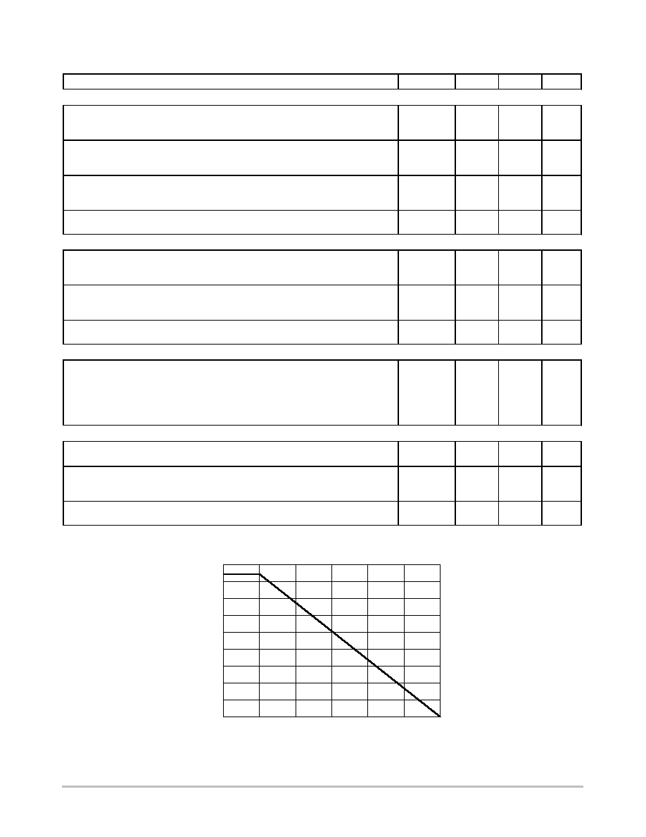
Figure 1. Power Temperature Derating Curve
T
C
, CASE TEMPERATURE (
∞
C)
P
D
, POWER DISSIP
A
TION (W
A
TTS)
80
70
50
30
10

BDW42* - NPN, BDW46, BDW47* - PNP
http://onsemi.com
3
Figure 2. Switching Times Test Circuit
5.0
0.1
Figure 3. Switching Times
I
C
, COLLECTOR CURRENT (AMP)
t, TIME
(s)
µ
3.0
0.7
0.5
0.3
0.2
0.05
0.2
0.3
0.7
3.0
10
t
d
@ V
BE(off)
= 0 V
V
CC
= 30 V
I
C
/I
B
= 250
I
B1
= I
B2
T
J
= 25
∞
C
t
f
0.07
1.0
5.0
t
s
t
r
0.1
1.0
2.0
0.5
2.0
7.0
0
V
CC
- 30 V
SCOPE
TUT
+ 4.0 V
t
r
, t
f
v 10 ns
DUTY CYCLE = 1.0%
R
C
D
1
MUST BE FAST RECOVERY TYPES, e.g.:
1N5825 USED ABOVE I
B
[ 100 mA
MSD6100 USED BELOW I
B
[ 100 mA
25
µ
s
D
1
51
R
B
AND R
C
VARIED TO OBTAIN DESIRED CURRENT LEVELS
V
2
APPROX
+ 8.0 V
V
1
APPROX
- 12 V
[ 8.0 k
[ 150
for t
d
and t
r
, D
1
id disconnected
and V
2
= 0
For NPN test circuit reverse all polarities
R
B
Figure 4. Thermal Response
t, TIME OR PULSE WIDTH (ms)
1.0
0.01
0.01
0.7
0.5
0.3
0.2
0.1
0.07
0.05
0.03
0.02
0.02
r(t) EFFECTIVE
TRANSIENT
THERMAL
RESIST
ANCE (NORMALIZED)
0.05
0.1
0.2
0.5
1.0
2.0
5.0
10
20
50
100
200
1000
500
R
JC
(t) = r(t) R
JC
R
JC
= 1.92
∞
C/W
D CURVES APPLY FOR POWER
PULSE TRAIN SHOWN
READ TIME AT t
1
T
J(pk)
- T
C
= P
(pk)
R
JC
(t)
P
(pk)
t
1
t
2
DUTY CYCLE, D = t
1
/t
2
D = 0.5
SINGLE PULSE
0.2
0.05
0.1
0.02
0.01
0.03
0.3
3.0
30
300

BDW42* - NPN, BDW46, BDW47* - PNP
http://onsemi.com
4
ACTIVE-REGION SAFE OPERATING AREA
SECOND BREAKDOWN LIMIT
BONDING WIRE LIMIT
THERMAL LIMITED
@ T
C
= 25
∞
C (SINGLE PULSE)
50
1.0
Figure 5. BDW42
20
2.0
0.05
10
20
100
T
J
= 25
∞
C
BDW42
1.0 ms
0.1 ms
0.2
5.0
0.5
I C
, COLLECT
OR CURRENT
(AMP)
V
CE
, COLLECTOR-EMITTER VOLTAGE (VOLTS)
10
30
70
1.0
0.1
0.5 ms
dc
2.0
50
3.0
5.0
7.0
Figure 6. BDW46 and BDW47
SECOND BREAKDOWN LIMIT
BONDING WIRE LIMIT
THERMAL LIMITED
@ T
C
= 25
∞
C (SINGLE PULSE)
50
1.0
20
2.0
0.05
10
20
100
T
J
= 25
∞
C
BDW46
BDW47
1.0 ms
0.1 ms
0.2
5.0
0.5
I C
, COLLECT
OR CURRENT
(AMP)
V
CE
, COLLECTOR-EMITTER VOLTAGE (VOLTS)
10
30
70
1.0
0.1
0.5 ms
dc
2.0
50
3.0
5.0
7.0
There are two limitations on the power handling ability of a
transistor: average junction temperature and second
breakdown. Safe operating area curves indicate I
C
- V
CE
limits
of the transistor that must be observed for reliable operation;
i.e., the transistor must not be subjected to greater dissipation
than the curves indicate. The data of Figure 5 and 6 is based on
T
J(pk)
= 200
_C; T
C
is variable depending on conditions.
Second breakdown pulse limits are valid for duty cycles to
10% provided T
J(pk)
v 200_C. T
J(pk)
may be calculated from
the data in Figure 4. At high case temperatures, thermal
limitations will reduce the power that can be handled to values
less than the limitations imposed by second breakdown.
*Linear extrapolation
10,000
1.0
Figure 7. Small-Signal Current Gain
f, FREQUENCY (kHz)
10
2.0
5.0
10
20
50
100
200
1000
500
300
100
5000
h
FE
, SMALL-SIGNAL
CURRENT
GAIN
20
3000
200
500
2000
1000
30
50
BDW46, 47 (PNP)
BDW42 (NPN)
T
J
= 25
∞
C
V
CE
= 3.0 V
I
C
= 3.0 A
300
0.1
Figure 8. Capacitance
V
R
, REVERSE VOLTAGE (VOLTS)
30
1.0
2.0
5.0
20
100
10
C, CAP
ACIT
ANCE (pF)
200
100
70
50
T
J
= + 25
∞
C
C
ib
C
ob
50
0.2
0.5
BDW46, 47 (PNP)
BDW42 (NPN)
BDW42* - NPN, BDW46, BDW47* - PNP
http://onsemi.com
5
0.1
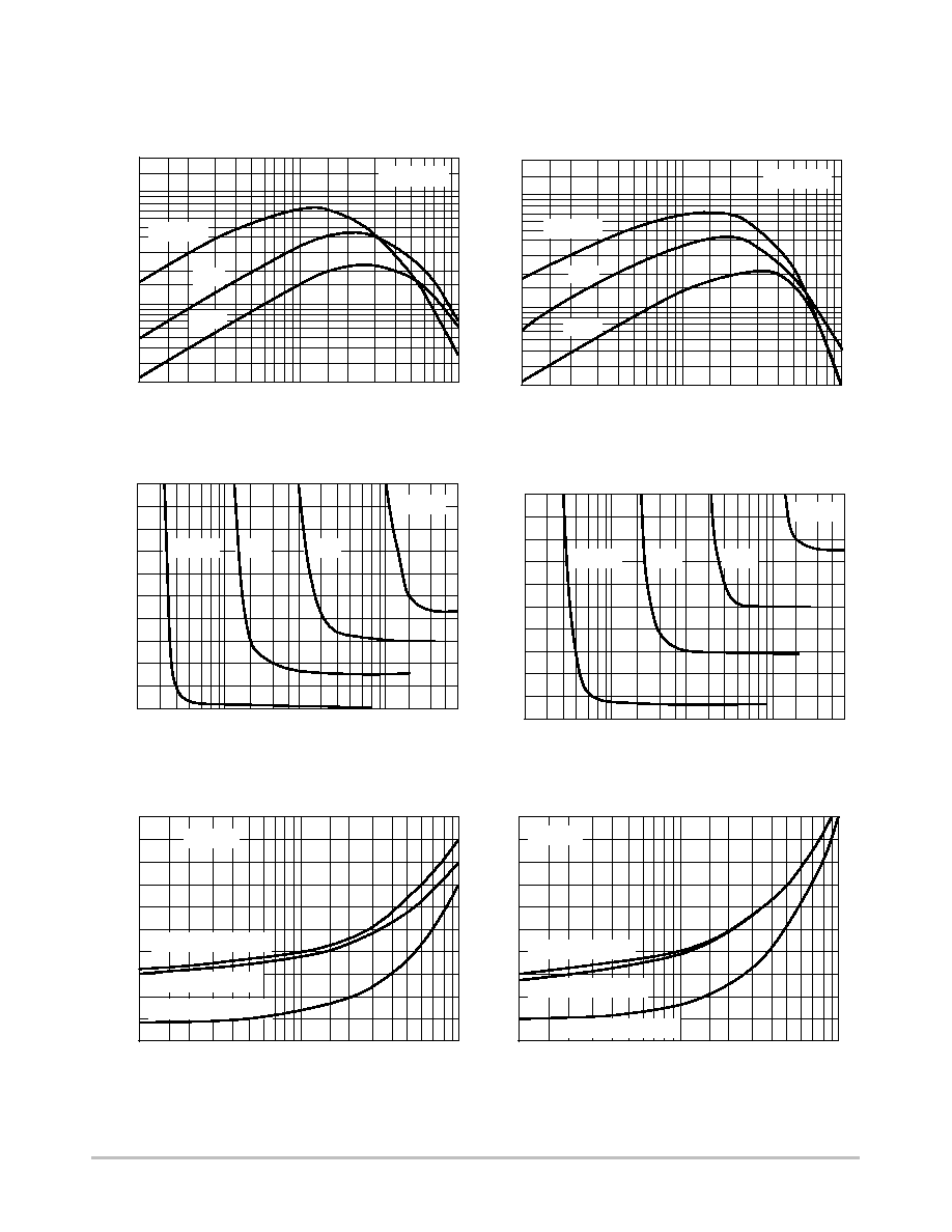
Figure 9. DC Current Gain
I
C
, COLLECTOR CURRENT (AMP)
0.2
0.3
0.5 0.7
1.0
2.0
10
500
300
h
FE
, DC CURRENT
GAIN
T
J
= 150
∞
C
25
∞
C
-55
∞
C
V
CE
= 3.0 V
200
7.0
BDW42 (NPN)
BDW46, 47 (PNP)
20,000
5000
10,000
3000
2000
1000
3.0
5.0
0.1
I
C
, COLLECTOR CURRENT (AMP)
0.2
0.3
0.5 0.7
1.0
2.0
10
500
300
h
FE
, DC CURRENT
GAIN
T
J
= 150
∞
C
25
∞
C
-55
∞
C
V
CE
= 3.0 V
200
7.0
20,000
5000
10,000
3000
2000
1000
3.0
5.0
7000
700
V
CE
, COLLECT
OR-EMITTER VOL
T
AGE (VOL
TS)
V
CE
, COLLECT
OR-EMITTER VOL
T
AGE (VOL
TS)
Figure 10. Collector Saturation Region
3.0
I
B
, BASE CURRENT (mA)
0.3
0.5
1.0
2.0 3.0
5.0 7.0
30
2.6
2.2
1.8
1.4
I
C
= 2.0 A
T
J
= 25
∞
C
4.0 A
6.0 A
1.0
0.7
20
10
3.0
I
B
, BASE CURRENT (mA)
0.3
0.5
1.0
2.0
3.0
5.0 7.0
30
2.6
2.2
1.8
1.4
I
C
= 2.0 A
T
J
= 25
∞
C
4.0 A
6.0 A
1.0
0.7
20
10
I
C
, COLLECTOR CURRENT (AMP)
V
BE(sat)
@ I
C
/I
B
= 250
V
,
VOL
T
AGE (VOL
TS)
Figure 11. "On" Voltages
I
C
, COLLECTOR CURRENT (AMP)
V
,
VOL
T
AGE (VOL
TS)
V
BE(sat)
@ I
C
/I
B
= 250
V
CE(sat)
@ I
C
/I
B
= 250
T
J
= 25
∞
C
V
BE
@ V
CE
= 4.0 V
V
BE
@ V
CE
= 4.0 V
V
CE(sat)
@ I
C
/I
B
= 250
T
J
= 25
∞
C
0.1
0.2 0.3
0.5 0.7
1.0
2.0
10
7.0
3.0
5.0
0.1
0.2 0.3
0.5 0.7 1.0
2.0
10
7.0
3.0
5.0
3.0
2.5
2.0
1.5
1.0
0.5
3.0
2.5
2.0
1.5
1.0
0.5

BDW42* - NPN, BDW46, BDW47* - PNP
http://onsemi.com
6
V
,
TEMPERA
TURE COEFFICIENT
(mV/
C)
∞
+5.0
Figure 12. Temperature Coefficients
I
C
, COLLECTOR CURRENT (AMP)
0.1
0.2 0.3
1.0
2.0 3.0
5.0
7.0
10
-55
∞
C to 25
∞
C
+4.0
+3.0
+1.0
0
-4.0
-1.0
-2.0
-3.0
-5.0
VB
for V
BE
*
VC
for V
CE(sat)
-55
∞
C to 25
∞
C
25
∞
C to 150
∞
C
25
∞
C to 150
∞
C
*I
C
/I
B
v 250
0.5 0.7
+5.0
I
C
, COLLECTOR CURRENT (AMP)
0.1
0.2 0.3
1.0
2.0 3.0
5.0
10
-55
∞
C to +25
∞
C
V
,
TEMPERA
TURE COEFFICIENTS (mV/
C)
∞
+4.0
+3.0
+1.0
0
-4.0
-1.0
-2.0
-3.0
-5.0
VB
for V
BE
*
VC
for V
CE(sat)
-55
∞
C to + 25
∞
C
+ 25
∞
C to 150
∞
C
+ 25
∞
C to 150
∞
C
*I
C
/I
B
v 250
0.5
+2.0
+2.0
BDW42 (NPN)
BDW46, 47 (PNP)
10
5
Figure 13. Collector Cut-Off Region
V
BE
, BASE-EMITTER VOLTAGE (VOLTS)
10
2
10
1
10
0
, COLLECT
OR CURRENT
(A)
µ
I C
10
- 1
-0.2 -0.4
0
+0.2
+0.4
+0.6
V
CE
= 30 V
T
J
= 150
∞
C
100
∞
C
25
∞
C
REVERSE
FORWARD
10
3
10
4
-0.6 -0.8
-1.0
-1.2 -1.4
10
5
V
BE
, BASE-EMITTER VOLTAGE (VOLTS)
10
2
10
1
10
0
, COLLECT
OR CURRENT
(A)
µ
I C
10
- 1
+0.2 +0.4
0
-0.2
-0.4
-0.6
V
CE
= 30 V
REVERSE
FORWARD
10
3
10
4
+0.6
+0.8
+1.0 +1.2 + 1.4
T
J
= 150
∞
C
100
∞
C
25
∞
C
Figure 14. Darlington Schematic
NPN
BDW42
PNP
BDW46
BDW47
BASE
COLLECTOR
EMITTER
[ 8.0 k
[ 60
BASE
COLLECTOR
EMITTER
[ 8.0 k
[ 60

BDW42* - NPN, BDW46, BDW47* - PNP
http://onsemi.com
7
PACKAGE DIMENSIONS
TO-220AB
CASE 221A-09
ISSUE AB
NOTES:
1. DIMENSIONING AND TOLERANCING PER ANSI
Y14.5M, 1982.
2. CONTROLLING DIMENSION: INCH.
3. DIMENSION Z DEFINES A ZONE WHERE ALL
BODY AND LEAD IRREGULARITIES ARE
ALLOWED.
DIM
MIN
MAX
MIN
MAX
MILLIMETERS
INCHES
A
0.570
0.620
14.48
15.75
B
0.380
0.405
9.66
10.28
C
0.160
0.190
4.07
4.82
D
0.025
0.035
0.64
0.88
F
0.142
0.147
3.61
3.73
G
0.095
0.105
2.42
2.66
H
0.110
0.155
2.80
3.93
J
0.018
0.025
0.46
0.64
K
0.500
0.562
12.70
14.27
L
0.045
0.060
1.15
1.52
N
0.190
0.210
4.83
5.33
Q
0.100
0.120
2.54
3.04
R
0.080
0.110
2.04
2.79
S
0.045
0.055
1.15
1.39
T
0.235
0.255
5.97
6.47
U
0.000
0.050
0.00
1.27
V
0.045
---
1.15
---
Z
---
0.080
---
2.04
B
Q
H
Z
L
V
G
N
A
K
F
1 2 3
4
D
SEATING
PLANE
-T-
C
S
T
U
R
J
STYLE 1:
PIN 1. BASE
2. COLLECTOR
3. EMITTER
4. COLLECTOR

BDW42* - NPN, BDW46, BDW47* - PNP
http://onsemi.com
8
ON Semiconductor and are registered trademarks of Semiconductor Components Industries, LLC (SCILLC). SCILLC reserves the right to make changes without further notice
to any products herein. SCILLC makes no warranty, representation or guarantee regarding the suitability of its products for any particular purpose, nor does SCILLC assume any liability
arising out of the application or use of any product or circuit, and specifically disclaims any and all liability, including without limitation special, consequential or incidental damages.
"Typical" parameters which may be provided in SCILLC data sheets and/or specifications can and do vary in different applications and actual performance may vary over time. All
operating parameters, including "Typicals" must be validated for each customer application by customer's technical experts. SCILLC does not convey any license under its patent rights
nor the rights of others. SCILLC products are not designed, intended, or authorized for use as components in systems intended for surgical implant into the body, or other applications
intended to support or sustain life, or for any other application in which the failure of the SCILLC product could create a situation where personal injury or death may occur. Should
Buyer purchase or use SCILLC products for any such unintended or unauthorized application, Buyer shall indemnify and hold SCILLC and its officers, employees, subsidiaries, affiliates,
and distributors harmless against all claims, costs, damages, and expenses, and reasonable attorney fees arising out of, directly or indirectly, any claim of personal injury or death
associated with such unintended or unauthorized use, even if such claim alleges that SCILLC was negligent regarding the design or manufacture of the part. SCILLC is an Equal
Opportunity/Affirmative Action Employer. This literature is subject to all applicable copyright laws and is not for resale in any manner.
PUBLICATION ORDERING INFORMATION
N. American Technical Support: 800-282-9855 Toll Free
USA/Canada
Japan: ON Semiconductor, Japan Customer Focus Center
2-9-1 Kamimeguro, Meguro-ku, Tokyo, Japan 153-0051
Phone: 81-3-5773-3850
BDW42/D
LITERATURE FULFILLMENT:
Literature Distribution Center for ON Semiconductor
P.O. Box 61312, Phoenix, Arizona 85082-1312 USA
Phone: 480-829-7710 or 800-344-3860 Toll Free USA/Canada
Fax: 480-829-7709 or 800-344-3867 Toll Free USA/Canada
Email: orderlit@onsemi.com
ON Semiconductor Website: http://onsemi.com
Order Literature: http://www.onsemi.com/litorder
For additional information, please contact your
local Sales Representative.