
©
Semiconductor Components Industries, LLC, 2001
September, 2001 ≠ Rev. 5
1
Publication Order Number:
CS51021A/D
CS51021A, CS51022A,
CS51023A, CS51024A
Enhanced Current Mode
PWM Controller
The CS51021A/2A/3A/4A Fixed Frequency PWM Current Mode
Controller family provides all necessary features required for AC≠DC
or DC≠DC primary side control. Several features are included
eliminating the additional components needed to implement them
externally. In addition to low start≠up current (75
µ
A) and high
frequency operation capability, the CS51021A/2A/3A/4A family
includes overvoltage and undervoltage monitoring, externally
programmable dual threshold overcurrent protection, current sense
leading edge blanking, current slope compensation, accurate duty cycle
control and an externally available 5.0 V reference. The CS51021A
and CS51023A feature bidirectional synchronization capability, while
the CS51022A and CS51024A offer a sleep mode with 100
µ
A
maximum IC current consumption. The CS51021A/2A/3A/4A family
is available in a 16 lead narrow body SO package.
Device
Sleep/Synch
V
CC
Start/Stop
CS51021A
Synch
8.25 V/7.7 V
CS51022A
Sleep
8.25 V/7.7 V
CS51023A
Synch
13 V/7.7 V
CS51024A
Sleep
13 V/7.7 V
Features
∑
75
µ
A Max. Startup Current
∑
Fixed Frequency Current Mode Control
∑
1.0 MHz Switching Frequency
∑
Undervoltage Protection Monitor
∑
Overvoltage Protection Monitor with Programmable Hysteresis
∑
Programmable Dual Threshold Overcurrent Protection with
Delayed Restart
∑
Programmable Soft Start
∑
Accurate Maximum Duty Cycle Limit
∑
Programmable Slope Compensation
∑
Leading Edge Current Sense Blanking
∑
1.0 A Sink/Source Gate Drive
∑
Bidirectional Synchronization (CS51021A/3A)
∑
50 ns PWM Propagation Delay
∑
100
µ
A Max Sleep Current (CS51022A/4A)
http://onsemi.com
x
= Specific Device Code
A
= Assembly Location
WL, L
= Wafer Lot
YY, Y
= Year
WW, W = Work Week
SO≠16
D SUFFIX
CASE 751B
1
16
V
FB
I
SET
1
CS5102xA
A
W
L
YWW
16
COMP
R
T
C
T
SS
OV
LGND
UV
V
REF
SLOPE
V
CC
SLEEP or SYNC
PGND
I
SENSE
V
C
GATE
PIN CONNECTIONS AND
MARKING DIAGRAM
Device
Package
Shipping
ORDERING INFORMATION*
CS51021AED16
SO≠16
48 Units/Rail
CS51021AEDR16
SO≠16
2500 Tape & Reel
CS51022AED16
SO≠16
48 Units/Rail
CS51022AEDR16
SO≠16
2500 Tape & Reel
CS51023AED16
SO≠16
48 Units/Rail
CS51023AEDR16
SO≠16
2500 Tape & Reel
CS51024AED16
SO≠16
48 Units/Rail
CS51024AEDR16
SO≠16
2500 Tape & Reel
* Consult your local sales representative for other
package options.

CS51021A, CS51022A, CS51023A, CS51024A
http://onsemi.com
2
V
C
V
REF
COMP
V
FB
R
T
C
T
SYNC/
C
SS
V
CC
UV
OV
I
SET
SLOPE
GATE
I
SENSE
PGND
CS51021A/2A
LGND
SLEEP
22 k
4700 pF
51 k
10 k
0.01
µ
F
24.3 k,
1.0%
200 k,
1.0%
2.49 k,
1.0%
BA521
IRF6345
6.98 k,
1.0%
6.98 k,
1.0%
470 pF
100 p
100
10 k
62
680 pF
100
µ
F 100
µ
F
V
OUT
SGND
(5 V/5 A)
10
FZT688
SYNC/SLEEP
22
µ
F
18 V
BAS21
51 k
11 V
(36 V to 72 V)
PGND
0.01
µ
F
1.0
µ
F
100
100:1
4:1
2:5
10
V
IN
MOC81025
TL431
1000 pF
5.1 k
0.1
µ
F
2.0 k, 1.0%
2.0 k,
1.0%
1.0 k
180
1.0 K
10 K
330 pF
Figure 1. Typical Application Diagram, 36≠72 V to 5.0 V, 5.0 A DC≠DC Converter
MAXIMUM RATINGS*
Rating
Value
Unit
Power Supply Voltage, V
CC
≠0.3, 20
V
Driver Supply Voltage, V
C
≠0.3, 20
V
SYNC, SLEEP, R
T
C
T
, SOFT START, V
FB
, SLOPE, I
SENSE
, UV, OV, I
SET
(Logic Pins)
0.25 to V
REF
V
Peak GATE Output Current
1.0
A
Steady State Output Current
±
0.2
A
Operating Junction Temperature, T
J
150
∞
C
Storage Temperature Range, T
S
≠65 to +150
∞
C
ESD (Human Body Model)
2.0
kV
Lead Temperature Soldering:
Reflow: (SMD styles only) (Note 1)
230 peak
∞
C
1. 60 second maximum above 183
∞
C.
*The maximum package power dissipation must be observed.
CS51021A, CS51022A, CS51023A, CS51024A
http://onsemi.com
3
ELECTRICAL CHARACTERISTICS
(Unless otherwise stated, specifications apply for ≠40
∞
C < T
A
< 85
∞
C,
≠40
∞
C < T
J
< 150
∞
C, 3.0 V < V
C
< 20 V, 8.2 V < V
CC
< 20 V, R
T
= 12 k
, C
T
= 390 pF)
Characteristic
Test Conditions
Min
Typ
Max
Unit
Under Voltage Lockout
START Threshold (CS51021A/2A)
≠
7.95
8.25
8.8
V
START Threshold (CS51023A/4A)
≠
12.4
13
13.4
V
STOP Threshold
≠
7.4
7.7
8.2
V
Hysteresis (CS51021A/2A)
≠
0.50
0.75
1.00
V
Hysteresis (CS51023A/4A)
≠
4.0
5.0
6.0
V
I
CC
@ Startup (CS51021A/2A)
V
CC
< UV
START
Threshold
≠
40
75
µ
A
I
CC
@ Startup (CS51023A/4A)
V
CC
< UV
START
Threshold
≠
45
75
µ
A
I
CC
Operating (CS51021A/3A)
≠
≠
7.0
9.0
mA
I
CC
Operating (CS51022A/4A)
≠
≠
6.0
8.0
mA
I
CC
Operating
Includes 1.0 nF Load
≠
7.0
12
mA
Voltage Reference
Initial Accuracy
T
A
= 25
∞
C, I
REF
= 2.0 mA, V
CC
= 14 V, Note 2
4.95
5.0
5.05
V
Total Accuracy
1.0 mA < I
REF
< 10 mA
4.9
5.0
5.15
V
Line Regulation
8.2 V < V
CC
< 18 V, I
REF
= 2.0 mA
≠
6.0
20
mV
Load Regulation
1.0 mA < I
REF
< 10 mA
≠
6.0
15
mV
NOISE Voltage
Note 2
≠
50
≠
µ
V
OP Life Shift
T = 1000 Hours, Note 2
≠
4.0
20
mV
FAULT Voltage
Force V
REF
0.90
◊
V
REF
0.93
◊
V
REF
0.95
◊
V
REF
V
OK Voltage
Force V
REF
0.94
◊
V
REF
0.96
◊
V
REF
0.985
◊
V
REF
V
OK Hysteresis
Force V
REF
75
165
250
mV
Current Limit
Force V
REF
≠20
≠
≠
mA
Error Amplifier
Initial Accuracy
T
A
= 25
∞
C, I
REF
= 2.0 mA, V
CC
= 14 V,
V
FB
= COMP, Note 2
2.465
2.515
2.565
V
Reference Voltage
V
FB
= COMP
2.440
2.515
2.590
V
V
FB
Leakage Current
V
FB
= 0 V
≠
≠0.2
≠2.0
µ
A
Open Loop Gain
1.4 V < COMP < 4.0 V, Note 2
60
90
≠
dB
Unity Gain Bandwidth
Note 2
1.5
2.5
≠
MHz
COMP Sink Current
COMP = 1.5 V, V
FB
= 2.7 V
2.0
6.0
≠
mA
COMP Source Current
COMP = 1.5 V, V
FB
= 2.3 V
≠0.2
≠0.5
≠
mA
COMP High Voltage
V
FB
= 2.3 V
4.35
4.8
5.0
V
COMP Low Voltage
V
FB
= 2.7 V
0.4
0.8
1.2
V
PS Ripple Rejection
FREQ = 120 Hz, Note 2
60
85
≠
dB
SS Clamp, V
COMP
V
SS
= 2.5 V, V
FB
= 0 V, I
SET
= 2.0 V
2.4
2.5
2.6
V
I
LIM(SET)
Clamp
Note 2
0.95
1.0
1.15
V
2. Guaranteed by design, not 100% tested in production.

CS51021A, CS51022A, CS51023A, CS51024A
http://onsemi.com
4
ELECTRICAL CHARACTERISTICS (continued)
(Unless otherwise stated, specifications apply for ≠40
∞
C < T
A
< 85
∞
C,
≠40
∞
C < T
J
< 150
∞
C, 3.0 V < V
C
< 20 V, 8.2 V < V
CC
< 20 V, R
T
= 12 k
, C
T
= 390 pF)
Characteristic
Unit
Max
Typ
Min
Test Conditions
Oscillator
Accuracy
R
T
= 12 k, C
T
= 390 pF
230
255
280
kHz
Voltage Stability
Delta Frequency 8.2 V < V
CC
< 20 V
≠
2.0
3.0
%
Temperature Stability
T
MIN
< T
A
< T
MAX,
Note
3
≠
8.0
≠
%
Min Charge & Discharge Time
Note 3
0.333
≠
≠
µ
s
Duty Cycle Accuracy
R
T
= 12 k, C
T
= 390 pF
70
77
83
%
Peak Voltage
Note 3
≠
3.0
≠
V
Valley Voltage
Note 3
≠
1.5
≠
V
Valley Clamp Voltage
10 k Resistor to ground on R
T
C
T
1.2
1.4
1.6
V
Discharge Current
≠
0.8
1.0
1.2
mA
Discharge Current
TA = 25
∞
C, Note 3
0.925
1.0
1.075
mA
Synchronization (CS51021A/3A)
Input Threshold
≠
1.0
1.5
2.7
V
Output Pulsewidth
≠
160
260
400
ns
Output High Voltage
I
SYNC
= 100
µ
A
3.5
4.3
4.8
V
Input Resistance
Note 3
35
70
140
k
Drive Delay
SYNC to GATE RESET
80
120
150
ns
Output Drive Current
1.0 k Load
1.25
2.0
3.5
mA
SLEEP (CS51022A/4A)
SLEEP Input Threshold
Active High
1.0
1.5
2.7
V
SLEEP Input Current
V
SLEEP
= 4.0 V
11
25
46
µ
A
I
CC
@ SLEEP
V
CC
15 V
≠
50
100
µ
A
GATE Driver
HIGH Voltage
Measure V
C
≠ GATE, V
C
= 10 V, 150 mA Load
≠
1.5
2.2
V
LOW Voltage
Measure GATE ≠ PGND, 150 mA SINK
≠
1.2
1.5
V
HIGH Voltage Clamp
V
C
= 20 V, 1.0 nF
11
13.5
16
V
LOW Voltage Clamp
Measured at 10 mA Output Current
≠
0.6
0.8
V
Peak Current
V
C
= 20 V, 1.0 nF, Note 3
≠
1.0
≠
A
UVL Leakage
V
C
= 20 V measured at 0 V
≠
≠1.0
≠50
µ
A
RISE Time
Load = 1.0 nF, 1.0 V < GATE < 9.0 V,
V
C
= 20 V, T
A
= 25
∞
C
≠
60
100
ns
FALL Time
Load = 1.0 nF, 9.0 V > GATE > 1 .0 V,
V
C
= 20 V
≠
15
40
ns
SLOPE Compensation
Charge Current
SLOPE = 2.0 V
≠63
≠53
≠43
µ
A
COMP Gain
Fraction of slope voltage added to I
SENSE
,
Note 3
0.095
0.100
0.105
V/V
Discharge Voltage
SYNC = 0 V
≠
0.1
0.2
V
3. Guaranteed by design, not 100% tested in production.

CS51021A, CS51022A, CS51023A, CS51024A
http://onsemi.com
5
ELECTRICAL CHARACTERISTICS (continued)
(Unless otherwise stated, specifications apply for ≠40
∞
C < T
A
< 85
∞
C,
≠40
∞
C < T
J
< 150
∞
C, 3.0 V < V
C
< 20 V, 8.2 V < V
CC
< 20 V, R
T
= 12 k
, C
T
= 390 pF)
Characteristic
Unit
Max
Typ
Min
Test Conditions
Current Sense
OFFSET Voltage
Note 4
0.09
0.10
0.11
V
Blanking Time
≠
≠
55
160
ns
Blanking Disable Voltage
Adjust V
FB
1.8
2.0
2.2
V
Second Current Threshold Gain
≠
1.21
1.33
1.45
V/V
I
SENSE
Input Resistance
≠
≠
5.0
≠
k
Minimum On Time
GATE High to Low
30
70
110
ns
Gain
Note 4
0.78
0.80
0.82
V/V
OV & UV Voltage Monitors
OV Monitor Threshold
≠
2.4
2.5
2.6
V
OV Hysteresis Current
≠
≠10
≠12.5
≠15
µ
A
UV Monitor Threshold
≠
1.38
1.45
1.52
V
UV Monitor Hysteresis
≠
25
75
100
mV
SOFT START (SS)
Charge Current
SS = 2.0 V
≠70
≠55
≠40
µ
A
Discharge Current
SS = 2.0 V
250
1000
≠
µ
A
Charge Voltage, V
SS
≠
4.4
4.7
5.0
V
Discharge Voltage, V
SS
≠
0.25
0.27
0.30
V
4. Guaranteed by design, not 100% tested in production.
PACKAGE PIN DESCRIPTION
PACKAGE PIN #
PIN SYMBOL
FUNCTION
16 Lead SO Narrow
1
GATE
External power switch driver with 1.0 A peak capability.
2
I
SENSE
Current sense amplifier input.
3
SYNC (CS51021A/3A)
Bi≠directional synchronization. Locks to the highest frequency.
3
SLEEP (CS51022A/4A)
Active high chip disable. In sleep mode, V
REF
and GATE are turned off.
4
SLOPE
Additional slope to the current sense signal. Internal current source
charges the external capacitor.
5
UV
Undervoltage protection monitor.
6
OV
Overvoltage protection monitor.
7
R
T
C
T
Timing resistor R
T
and capacitor C
T
determine oscillator frequency and
maximum duty cycle, D
MAX.
8
I
SET
Voltage at this pin sets pulse≠by≠pulse overcurrent threshold, and sec-
ond threshold (1.33 times higher) with Soft Start retrigger (hiccup mode).
9
V
FB
Feedback voltage input. Connected to the error amplifier inverting input.
10
COMP
Error amplifier output. Frequency compensation network is usually
connected between COMP and V
FB
pins.
11
SS
Charging external capacitor restricts error amplifier output voltage dur-
ing the start or fault conditions (hiccup).
12
LGND
Logic ground.

CS51021A, CS51022A, CS51023A, CS51024A
http://onsemi.com
6
PACKAGE PIN DESCRIPTION (continued)
PACKAGE PIN #
FUNCTION
PIN SYMBOL
16 Lead SO Narrow
13
V
REF
5.0 V reference voltage output.
14
V
CC
Logic supply voltage.
15
PGND
Output power stage ground connection.
16
V
C
Output power stage supply voltage.
D
2
Start
+
≠
Stop
SS
+
≠
Clamp
E/A
+
≠
I
SET
≠
+
Clamp
D
3
D
1
20 k
10 k
V
FB
≠
+
Monitor
G
4
PWM
≠
+
Comp
55 ns
Blank
I
SENSE
SLOPE
V
FB
COMP
R
T
C
T
2nd
+
≠
Threshold
OV
+
≠
Monitor
DISABLE
0.1
0.8
Q
2
1.33
53
µ
A
I
SET
OV
12.5
µ
A
V
REF
2.5 V
+
≠
+
≠
2.0 V
+
≠
2.5 V
V
REF
V
ISENSE
SS
≠
+
Monitor
Discharge
Latch
UV
≠
+
Monitor
1.45 V
+
≠
4.7 V
+
≠
S
R
Q
F
1
G
1
G
2
D
4
ZD
1
13.5 V
V
C
GATE
PGND
SS
UV
G
3
FAULT
55
µ
A
V
REF
OSC
SYNC
4.3 V
200 ns
≠
+
V
REF
_OK
+
≠
4.75 V
V
REF
= 5.0 V
+
≠
+
≠
0.1 V
V
CC
_OK
V
REF
SLEEP
LGND
V
CC
Figure 2. Block Diagram
CS51021A, CS51022A, CS51023A, CS51024A
http://onsemi.com
7
CIRCUIT DESCRIPTION
SYNC
R
T
C
T
SLOP
E
IS
V
DS
0 V
0 V
0 V
0 V
0 V
V
IN
0 V
V
COMP
PWM COMP
GATE
4.3 V
200 ns
T
CH
T
DIS
V
SLOPE
55 ns
Blanking
IS + 0.1 SLOPE
IS
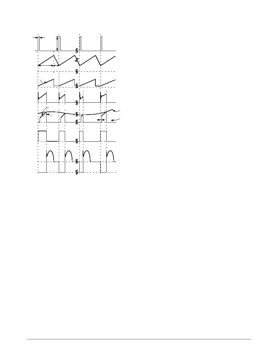
Figure 3. Typical Waveforms
THEORY OF OPERATION
Powering the IC
The IC has two supply and two ground pins. V
C
and
PGND pins provide high speed power drive for the external
power switch. V
CC
and LGND pins power the control
portion of the IC. The internal logic monitors the supply
voltage, V
CC
. During abnormal operating conditions, the
output is held low. The CS51021A/2A/3A/4A requires only
75
µ
A of startup current.
Voltage Feedback
The output voltage is monitored via the V
FB
pin and is
compared with the internal 2.5 V reference. The error
amplifier output minus one diode drop is divided by 3 and
connected to the negative input of the PWM comparator.
The positive input of the PWM comparator is connected to
the modified current sense signal. The oscillator turns the
external power switch on at the beginning of each cycle.
When current sense ramp voltage exceeds the reference side
of PWM comparator, the output stage latches off. It is turned
on again at the beginning of the next oscillator cycle.
Current Sense and Protection
The current is monitored at the I
SENSE
pin. The
CS51021A/2A/3A/4A has leading edge blanking circuitry
that ignores the first 55 ns of each switching period.
Blanking is disabled when V
FB
is less than 2.0 V so that the
minimum on≠time of the controller does not have an
additional 55 ns of delay time during fault conditions. For
the remaining portion of the switching period, the current
sense signal, combined with a fraction of the slope
compensation voltage, is applied to the positive input of the
PWM comparator where it is compared with the divided by
three error amplifier output voltage. The pulse≠by≠pulse
overcurrent protection threshold is set by the voltage at the
I
SET
pin. This voltage is passed through the I
SET
Clamp and
appears at the non≠inverting input of the PWM comparator,
limiting its dynamic range according to the following
formula:
Overcurrent Threshold
+
0.8
VI(SENSE)
)
0.1 V
)
0.1 VSLOPE
where
VI(SENSE) is voltage at the ISENSE pin.
and
VSLOPE is voltage at the SLOPE pin.
During extreme overcurrent or short circuit conditions,
the slope of the current sense signal will become much
steeper than during normal operation. Due to loop
propagation delay, the sensed signal will overshoot the
pulse≠by≠pulse threshold eventually reaching the second
overcurrent protection threshold which is 1.33 times higher
than the first threshold and is described by the following
equation:
2nd Threshold
+
1.33
VI(SET)
Exceeding the second threshold will reset the Soft Start
capacitor C
SS
and reinitiate the Soft Start sequence,
repeating for as long as the fault condition persists.
Soft Start
During power up, when the output filter capacitor is
discharged and the output voltage is low, the voltage across
the Soft Start capacitor (V
SS
) controls the duty cycle. An
internal current source of 55
µ
A charges C
SS
. The maximum
error amplifier output voltage is clamped by the SS Clamp.
When the Soft Start capacitor voltage exceeds the error
amplifier output voltage, the feedback loop takes over the
duty cycle control. The Soft Start time can be estimated with
the following formula:
tSS
+
9
10
4
CSS
The Soft Start voltage, V
SS
, charges and discharges
between 0.25 V and 4.7 V.

CS51021A, CS51022A, CS51023A, CS51024A
http://onsemi.com
8
Slope Compensation
DC≠DC converters with current mode control require a
current sense signal with slope compensation to avoid
instability at duty cycles greater than 50%. Slope capacitor
C
S
is charged by an internal 53
µ
A current source and is
discharged during the oscillator discharge time. The slope
compensation voltage is divided by 10 and is added to the
current sense voltage, V
I(SENSE)
. The signal applied to the
input of the PWM comparator is a combination of these two
voltages. The slope compensation, dV
SLOPE
/dt
,
is
calculated using the following formula:
dVSLOPE
dt
+
0.1
53
m
A
CS
It should be noted that internal capacitance of the IC will
cause an error when determining slope compensation
capacitance C
S
. This error is typically small for large values
of C
S
, but increases as C
S
becomes small and comparable to
the internal capacitance. The effect is apparent as a reduction
in charging current due to the need to charge the internal
capacitance in parallel with C
S
.Figure 4 shows a typical
curve indicating this decrease in available charging current.
Figure 4. The Slope Compensation Pin Charge
Current Reduces When a Small Capacitor Is Used.
10
100
1000
60
55
50
45
40
35
30
25
20
Charging
Current (
µ
A)
Compensation Cap (pF)
Undervoltage (UV) and Overvoltage (OV) Monitor
Two independent comparators monitor OV and UV
conditions. A string of three resistors is connected in series
between the monitored voltage (usually the input voltage)
and ground (see Figure 5). When voltage at the OV pin
exceeds 2.5 V, an overvoltage condition is detected and
GATE shuts down. An internal 12.5
µ
A current source turns
on and feeds current into the external resistor, R
3
, creating
a hysteresis determined by the value of this resistor (the
higher the value, the greater the hysteresis). The hysteresis
voltage of the OV monitor is determined by the following
formula:
VOV(HYST)
+
12.5
m
A
R3
where R
3
is a resistor connected from the OV pin to ground.
When the monitored voltage is low and the UV pin is less
than 1.45 V, GATE shuts down. The UV pin has fixed 75 mV
hysteresis.
Both OV and UV conditions are latched until the Soft Start
capacitor is discharged. This way, every time a fault
condition is detected the controller goes through the power
up sequence.
Figure 5. UV/OV Monitor Divider
V
IN
V
UV
V
OV
R
1
R
2
R
3
To calculate the OV?UV resistor divider :
1. Solve for R
3
, based on OV hysteresis requirements.
R3
+
VOV(HYST)
2.5 V
VMAX
12.5
m
A
where V
OV(HYST)
is the desired amount of
overvoltage
hysteresis, and V
MAX
is the input voltage
at which the supply will shut down.
2. Find the total impedance of the divider.
RTOT
+
R1
)
R2
)
R3
+
VMAX
R3
2.5
3. Determine the value of R
2
from the UV threshold
conditions.
R2
+
1.45
RTOT
VMIN
*
R3
where V
MIN
is the UV voltage at which the supply
will shut down.
4. Calculate R
1
.
R1
+
RTOT
*
R2
*
R3
5. The undervoltage hysteresis is given by :
VUV(HYST)
+
VMIN
0.075
1.45
V
REF
Monitor
The 5.0 V reference voltage is internally monitored to
ensure that it remains within specifications. The monitor,
which outputs a fault, can be tripped by two methods:
∑
If the reference voltage drops below 4.75 V
∑
If V
CC
falls below the STOP threshold
As indicated in the block diagram, any fault causes the
output to stop switching and begins the discharge of the Soft
Start capacitor C
SS
.

CS51021A, CS51022A, CS51023A, CS51024A
http://onsemi.com
9
Synchronization
A bi≠directional synchronization is provided to
synchronize several controllers. When SYNC pins are
connected together, the converters will lock to the highest
switching frequency. The fastest controller becomes the
master, producing a 4.3 V, 200 ns pulse train. Only one, the
highest frequency SYNC signal, will appear on the SYNC
line.
Sleep
The sleep input is an active high input. The CS51022A/4A
is placed in sleep mode when SLEEP is driven high. In sleep
mode, the controller and MOSFET are turned off. Connect
to GND for normal operation. The sleep mode operates at
VCC
15 V.
Oscillator and Duty Cycle Limit
The switching frequency is set by R
T
and C
T
connected to
the R
T
C
T
pin. C
T
charges and discharges between 3.0 V and
1.5 V.
The maximum duty cycle is set by the ratio of the on time,
t
ON
, and the whole period, T = t
ON
+ t
OFF
. Because the
timing capacitor's discharge current is trimmed, the
maximum
duty cycle is well defined. It is determined by the
ratio between the timing resistor R
T
and the timing capacitor
C
T
. Refer to figures 6 and 7 to select appropriate values for
R
T
and C
T
.
fSW
+
1
TSW
; TSW
+
tCH
)
tDIS
5
2500
Frequency
(kHz)
R
T
(k
)
2000
1500
1000
500
0
100
90
80
70
60
50
40
10
15
20
25
30
35
40
45
50
5
10
15
20
25
30
35
40
45
50
55
R
T
(k
)
Duty Cycle (%)
1
2
3
4
5
6
8
7
2
1
3
4
8
7
5
6
1. C
T
= 47 pF
2. C
T
= 100 pF
3. C
T
= 150 pF
4. C
T
= 220 pF
5. C
T
= 390 pF
6. C
T
= 470 pF
7. C
T
= 560 pF
8. C
T
= 680 pF
1. C
T
= 47 pF
2. C
T
= 100 pF
3. C
T
= 150 pF
4. C
T
= 220 pF
5. C
T
= 390 pF
6. C
T
= 470 pF
7. C
T
= 560 pF
8. C
T
= 680 pF
Figure 6. Frequency vs. R
T
for Discrete
Capacitor Values
Figure 7. Duty Cycle vs. R
T
for Discrete
Capacitor Values

CS51021A, CS51022A, CS51023A, CS51024A
http://onsemi.com
10
PACKAGE DIMENSIONS
NOTES:
1. DIMENSIONING AND TOLERANCING PER ANSI
Y14.5M, 1982.
2. CONTROLLING DIMENSION: MILLIMETER.
3. DIMENSIONS A AND B DO NOT INCLUDE
MOLD PROTRUSION.
4. MAXIMUM MOLD PROTRUSION 0.15 (0.006)
PER SIDE.
5. DIMENSION D DOES NOT INCLUDE DAMBAR
PROTRUSION. ALLOWABLE DAMBAR
PROTRUSION SHALL BE 0.127 (0.005) TOTAL
IN EXCESS OF THE D DIMENSION AT
MAXIMUM MATERIAL CONDITION.
1
8
16
9
SEATING
PLANE
F
J
M
R
X 45
_
G
8 PL
P
≠B≠
≠A≠
M
0.25 (0.010)
B
S
≠T≠
D
K
C
16 PL
S
B
M
0.25 (0.010)
A
S
T
DIM
MIN
MAX
MIN
MAX
INCHES
MILLIMETERS
A
9.80
10.00
0.386
0.393
B
3.80
4.00
0.150
0.157
C
1.35
1.75
0.054
0.068
D
0.35
0.49
0.014
0.019
F
0.40
1.25
0.016
0.049
G
1.27 BSC
0.050 BSC
J
0.19
0.25
0.008
0.009
K
0.10
0.25
0.004
0.009
M
0
7
0
7
P
5.80
6.20
0.229
0.244
R
0.25
0.50
0.010
0.019
_
_
_
_
SO≠16
D SUFFIX
CASE 751B≠05
ISSUE J
PACKAGE THERMAL DATA
Parameter
SO≠16
Unit
R
JC
Typical
28
∞
C/W
R
JA
Typical
115
∞
C/W

CS51021A, CS51022A, CS51023A, CS51024A
http://onsemi.com
11
Notes

CS51021A, CS51022A, CS51023A, CS51024A
http://onsemi.com
12
ON Semiconductor and are trademarks of Semiconductor Components Industries, LLC (SCILLC). SCILLC reserves the right to make changes
without further notice to any products herein. SCILLC makes no warranty, representation or guarantee regarding the suitability of its products for any particular
purpose, nor does SCILLC assume any liability arising out of the application or use of any product or circuit, and specifically disclaims any and all liability,
including without limitation special, consequential or incidental damages. "Typical" parameters which may be provided in SCILLC data sheets and/or
specifications can and do vary in different applications and actual performance may vary over time. All operating parameters, including "Typicals" must be
validated for each customer application by customer's technical experts. SCILLC does not convey any license under its patent rights nor the rights of others.
SCILLC products are not designed, intended, or authorized for use as components in systems intended for surgical implant into the body, or other applications
intended to support or sustain life, or for any other application in which the failure of the SCILLC product could create a situation where personal injury or
death may occur. Should Buyer purchase or use SCILLC products for any such unintended or unauthorized application, Buyer shall indemnify and hold
SCILLC and its officers, employees, subsidiaries, affiliates, and distributors harmless against all claims, costs, damages, and expenses, and reasonable
attorney fees arising out of, directly or indirectly, any claim of personal injury or death associated with such unintended or unauthorized use, even if such claim
alleges that SCILLC was negligent regarding the design or manufacture of the part. SCILLC is an Equal Opportunity/Affirmative Action Employer.
PUBLICATION ORDERING INFORMATION
JAPAN: ON Semiconductor, Japan Customer Focus Center
4≠32≠1 Nishi≠Gotanda, Shinagawa≠ku, Tokyo, Japan 141≠0031
Phone: 81≠3≠5740≠2700
Email: r14525@onsemi.com
ON Semiconductor Website: http://onsemi.com
For additional information, please contact your local
Sales Representative.
CS51021A/D
Literature Fulfillment:
Literature Distribution Center for ON Semiconductor
P.O. Box 5163, Denver, Colorado 80217 USA
Phone: 303≠675≠2175 or 800≠344≠3860 Toll Free USA/Canada
Fax: 303≠675≠2176 or 800≠344≠3867 Toll Free USA/Canada
Email: ONlit@hibbertco.com
N. American Technical Support: 800≠282≠9855 Toll Free USA/Canada